Jackson M.J. Micro and Nanomanufacturing
Подождите немного. Документ загружается.

Principles of Micro- and Nanofabrication 51
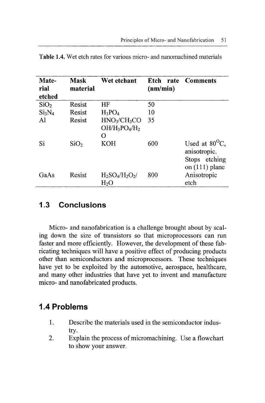
Table 1.4. Wet etch rates for various micro- and nanomachined materials
Mate-
rial
etched
Si02
Si3N4
Al
Si
GaAs
Mask
material
Resist
Resist
Resist
Si02
Resist
Wet etcliant
HF
H3PO4
HNO3/CH3CO
OH/H3PO4/H2
0
KOH
H2SO4/H2O2/
H2O
Etch
rate
(nm/min)
50
10
35
600
800
Comments
Used at 80*^C,
anisotropic.
Stops etching
on (111) plane
Anisotropic
etch
1.3 Conclusions
Micro- and nanofabrication is a challenge brought about by scal-
ing down the size of transistors so that microprocessors can run
faster and more efficiently. However, the development of these fab-
ricating techniques will have a positive effect of producing products
other than semiconductors and microprocessors. These techniques
have yet to be exploited by the automotive, aerospace, healthcare,
and many other industries that have yet to invent and manufacture
micro- and nanofabricated products.
1.4 Problems
1.
Describe the materials used in the semiconductor indus-
try.
2.
Explain the process of micromachining. Use a flowchart
to show your answer.
52 Micro- and Nanomanufacturing
3.
Explain how deep trenches are machined in sihcon.
4.
Illustrate how microcapacitors are manufactured.
5.
Show how cantilever probes for AFM applications are
manufactured using deep reactive ion etching.
6. Describe and illustrate the basic chipmaking process.
7.
What is soft lithography? How does soft lithography
overcome the problems encountered using optical lithog-
raphy?
8. Show how field effect transistors are manufactured using
soft lithographic techniques.
9. Explain the operation of a scanning tunneling micro-
scope.
10.
What is an atomic force microscope? Explain its modes
of operation.
11.
Explain how carbon nanotubes can be used to make field
effect transistors.
12.
Describe the properties of carbon nanotubes.
13.
How are carbon nanotubes used to make AFM probes?
14.
Show how a field effect transistor, variable area capaci-
tor, and electronic resonators are manufactured.
References
1.
Campbell SA, The Science and Engineering of Microelec-
tronic Fabrication - 2nd Edition, Oxford Series in Electrical
Engineering - Oxford University Press, 2005.
2.
Yeager RC, Introduction to Microelectronic Fabrication, Vol-
ume V, Modular Series on Solid State Devices - edited by
Neudeck and Pierret, Addison Wesley Press, Reading, MA,
1988.
3.
Sun
Y,
H. von
Zeigl,
J. L. Tauritz, R. Baets, Suspended Mem-
brane Inductors and Capacitors for Application in Silicon
MMCs, Microwave and Monolithic Circuits Symposium Di-
gest of Papers, IEEE,
p.p.
99-102, 1996.
4.
Piazza GR, R. Abdolvand, and
F.
Ayazi, Voltage-Tunable,
Piezoelectrically-Transduced Single Crystal Silicon Resona-
tors on SOI Substrates, 2003 IEEE MEMS Conference, Kyoto,
Japan,
p.p.
149-152,2003.
Principles of Micro- and Nanofabrication 53
5.
Deep Reactive Ion Etching Patent Number 5501893, Robert
Bosch GmbH, 1996.
6. Yao JJ, Topical Review: RF MEMS from a Device Perspec-
tive,
Journal of Micromechanics and Microengineering, 10,
R9-R38,
2000.
7.
Hutcheson GD, The First Nanochips, Scientific American, p.p.
76-83,
April 2004.
8. Taur Y, IBM Journal of Research and Development, 46, 2/3,
2002.
9. lonescu AM et al.. Few Electron Devices - Towards Hybrid
CMOS-SET Integrated Circuits, Proc. 39* Design and Auto-
mation Conference, New Orleans, USA, p.p.
88-93,
2002.
10.
Whitesides GM and Love JC, The Art of Building Small, Sci-
entific American - Special Issue on Nanotechnology, p.p. 39-
47,
September 2001.
11.
Hu J et al.. Using Soft Lithography to Fabricate GaAs/AlGaAs
Heterostructure Field Effect Transistors, Applied Physics Let-
ters,
71, (14), October 1997.
12.
Giessibl FJ, Advances in Atomic Force Microscopy, Accessed
on line at: xxx.lanl.gov/arXiv:cond-mat/0305119. Accessed
December 2005.
13.
Crommie MF, Lutz CP, Eigler DM, Science, 262, 218-220,
1993.
14.
Braun KF and Reider KH, Phys. Rev. Lett, 88,
096801,
2002.
15.
Marcus R, Ravi T, Gmitter K, Chin K, Liu D, Orvis W, Ciarlo
D,
Hunt C, Truijillo J, Formation of Silicon Tips with Inm
Radius, Appl. Phys. Lett., 56, (3), 236-238, 1990.
16.
Giessibl FJ and Binnig G, True Atomic Resolution on KBr
with a Low Temperature Atomic Force Microscope in Ultra
High Vacuum, Ultramicroscopy, 42-44, 281-286, 1992.
17.
Giessibl FJ and Trafas BM, Piezoresistive Cantilevers Utilized
for Scanning Tunneling and Scanning Force Microscopes in
Ultra High Vacuum, Rev. Sci. Instrum., 65, 1923-1929, 1994.
18.
Erlandsson R, Olsson L, and Martensson P, Inequivalent At-
oms and Imaging Mechanisms in AC-Mode Atomic Force Mi-
croscopy, Phys. Rev. B., 54, R8309-R8312. 1994.
19.
Lantz M, Hug HJ, Hoffman P, van Schendel P, Kappenberger
P,
Martin S, Baratoff A, and Gunderrodt H, Quantitative
Measurement of Short-Range Chemical Bonding Forces, Sci-
ence,
291, 2580-2583, 2001.
54 Micro-
and
Nanomanufacturing
20.
Patrin
J,
Atomic Resolution
of
an Insulator
by
Non-contact
AFM,
12*^
International Conference
on
Scanning Tunneling
Microscopy, Colorado,
1995.
21.
Requicha A, Nanorobots, NEMS, and Nanoassembly, Pro-
ceedings of the IEEE Special issue
on
nanoelectronics
and
nanoprocessing,
91,
(11), p.p. 1922-1933, November
2003.
www-lmr.usc.edu/~lmr/html/publications.html. Accessed
De-
cember 2005.
22.
Bezyadin
A,
Dekker
C,
Scmid
G,
Electrostatic Trapping
of
Single Conducting Nanoparticles Between Nanoelectrodes,
Appl. Phys. Lett., 71,
(9),
September
1997.
23.
Avouris
P et
al.. Applied
Surf. Sci.,
141, 210-209,
1999.
24.
Wang
X,
Bullen
D, Zou J, Ryu K,
Chung SW,
and
Mirkin
CA,
Linear Arrays
for Dip
Pen Nanolithography, Materials
Re-
search Bull.,
26,
(7), p.p. 535-538, July 2001.
25.
Dresselhaus
M,
January 1998
-
Website accessed December
2005.
http://http://phvsicsweb.org/article/world/n
1/1/9.
26.
Fukuda
H,
Arai
J, and
Dong
K,
Assembly of Nanodevices
with Carbon Nanotubes Through Nanorobotic Manipulators,
Proc.
IEEE,
91,
(11), p.p. 1803-1818, November
2003.
27.
Cheung CL, Hafner
J,
Lieber CM, Carbon Nanotube Atomic
Force Microscopy Tips: Direct Growth
By
Chemical Vapor
Deposition
and
Application
to
High Resolution Imaging,
PNAS,
97,
(8), p. 3813, April 11, 2000.
28.
Bachtold
A et
al.. Science, 294, p.l317, 2000.
29.
Derycke
V,
Martel
R,
Appenzeller
J, and
Avouris
P,
Carbon
Nanotube Inter
and
Intramolecular Logic Gates, Nano Letters,
1,
p.p. 453-456, 2001.
2.
Microfabrication Using X- ray
Lithography
2.1 Introduction
During the last decade there has been a rapid development in micro-
fabrication technology driven by the market need for low-cost con-
sumer products such as portable telecommunications equipment,
computers, and healthcare diagnostics. Much of the technology used
for these is based on production of silicon semiconductors and mi-
crochips. Interest in non-silicon-based technologies started to grow
back in the early 1980s with the development of a German fabrica-
tion process known as LIGA, an acronym for Lithography (LJtho-
graphie), electroplating (Galvanoformung), molding (Abformung)
[1,2].
It originated at the Karlsruhe Nuclear Research Laboratory in
Germany. Since then a number of groups, mainly in Germany and
the United States have been active in developing the process to make
precision microcomponents for a range of innovative products such
as microspectrometers, fiber-optic wave guides, micro-reactors and
microfluidic devices. A few of these have been manufactured on a
large scale and placed on the market. LIGA was often used to fabri-
cate the components, which were then integrated with others into the
end product. High costs are often associated with the integration
and packaging of the final product.
The most active groups developing and using the LIGA process
are the Sandia National Laboratories at Livermore, the Center for
Advanced Microstructures and Devices (CAMD) at the Louisiana
State University at Baton Rouge, in the United States, Institut fur
Mikrostrukturtechnik (FZK) Karlsruhe and Antwenderzentrum
BESSY, Berlin in Germany. In addition the work done in the United
Kingdom at Central Microstructure Facility at the CCLRC's Ruther-
ford Appleton Laboratory using the national synchrotron at Dares-
56 Micro- and Nanomanufacturing
bury as part of a European network program has advanced fabrica-
tion techniques in mask and resist development. A small start in
commercialization has been made by two companies in the United
States, Axsun and International Mezzo, which provides commercial
LIGA services.
Progress in commercialization has been slow owing to the ab-
sence of fast prototyping and large- scale manufacturing capabilities,
and the lack of established design rules and standards. This situation
was recently reviewed at a workshop at the COMS2004 conference
in Edmonton. The delegates decided to form an International LIGA
Interest Group to bring together major researchers, practitioners,
manufacturers, and users into an international network to provide
mechanisms for communication to solve the problems and be an in-
centive for commercialization.
Since 1980 numerous reports and papers on the development and
use of the LIGA process have been published and are too numerous
to be listed here. A more recent overview of the current status of this
process was given by Hruby at the HARMST Conference in 2003
[3],
and commercialization issues were reviewed recently by Tolfree
at COMS2004 [4] and Goettert at COMS2004 [5].
The latest market survey [6] indicated that a global market val-
ued in excess $40 billion is emerging for microproducts. The in-
creased interest in nanotechnology driven by the prospect of produc-
ing new non-silicon-based materials with unique properties, has
increased market estimates to over a $1 trillion. Micro-
nanomanufacturing is now a key value-added element in many sec-
tors of industry.
The boundaries between nanotechnology and microtechnology
may be blurred, but there is a degree of commonality in the tech-
niques and equipment involved in both - but they are, in essence and
in application, very different. It is at the nano not the micro scale
that the physical and chemical properties of materials change. Mi-
crofabrication is essentially a top-down technology but at the nano-
scale, either top-down or bottom-up techniques can be used, and the
latter are significantly different. Many products require a variety of
top-down processes for their manufacture. For example, the com-
mon CD has data pits about 500 nm wide and 125 nm deep formed
Microfabrication Using X- ray Lithography 57
in a plastic disc. The read-write heads are very precise mechanisms
that require a number of electro- mechanical processes.
Extensive papers and reviews on microfabrication technologies
have been published. Two examples are: "The Fundamentals of Mi-
crofabrication" by Madou 2002 [7], and 'Microfabrication using
Synchrotron Radiation" by Tolfree in 1998 [8]. These and others can
be found in the literature and on internet sites, cover most of the
relevant principles and issues associated with the development and
exploitation of the technologies. It was therefore decided to restrict
the content on this chapter to microfabrication using lithographic X-
ray techniques. This technique is known as deep X- ray lithography
(DXRL), is like all lithographic processes, ultimately limited in line-
width by the wavelength of the illuminating radiation. The conver-
sion from a 2-D pattern to a 3-D structure is dependent on a number
of factors, which are examined below.
There are multiple types of lithography, including UV, deep UV,
X- ray and electron-beam lithography. Currently, for non-silicon-
based materials, the highest precision can be achieved using DXRL
with very parallel, high-energy x- rays from a synchrotron radiation
source (SRS). It is the increased access provided by the large num-
ber (>80) of synchrotrons now operating world wide, coupled to
availability of low-solubility resists, thus reducing exposure time
that has encouraged a greater interest in DXRL. This technique still
has to find a wider community of users outside of research but it will
have a significant role to play in the range of tools and processes re-
quired to develop a micro-nanotechnology (MNT)-based industry.
Micro-nanotechnology (MNT) is pervasive and will have an im-
pact, sometimes disruptive, on almost every industry sector and
through the generation of new products and systems, on the society
in general. The universal use of the mobile telephone and ink-jet
printer are two well-known examples. The availability of a vast
range of new consumer and industrial products such as sensors, em-
bedded transducers and actuators, displays, health care diagnostics
etc.
will revolutionize the way people will live and work in the fu-
ture.
58 Micro-and Nanomanufacturing
2.2 X- ray Lithography
2.2.1.
History
International Business Machines (IBM) first combined electrode-
position and
X-
ray lithography in 1969. They made high-aspect ratio
metal structures by plating gold patterns of 20 jum in thickness in a
resist that had been exposed to x- rays. The IBM work was an ex-
tension of through-mask plating, also pioneered by IBM in 1969,
and was directed toward the fabrication of thin film magnetic re-
cording heads. A historical background of lithography was provided
by Cerrina [9].
The development of the LIGA process referred to above required
small slotted nozzles for uranium isotope separation [10] to be pro-
duced. Since then, the X- ray lithographic technique has been de-
veloped to fabricate a variety of microstructures in materials [11 -
19].
The potential of LIGA for the development of microsystems
was reviewed by Bacher [20]. Essentially, a three-step process, the
LIGA technique can be used to make 3D microstructures.
By adding molding techniques the broader implications of x- ray
lithography as a means of low-cost manufacturing of a wide variety
of microparts with unprecedented accuracy from various materials
can be realised. In Germany, x- ray lithography was originally de-
veloped outside of the semiconductor industry.
Early pioneering work in the use of synchrotron radiation for
microfabrication was carried out by Professor Guckel at the Univer-
sity of Wisconsin in the United States. This included use of the
LIGA technique to develop micromotors [21-24]. Guckel reposi-
tioned the field in light of semiconductor process capabilities and
brought it closer to standard manufacturing processes.
Microfabrication Using X- ray Lithography 59
2.3 Synchrotron Radiation (SR)
2.3.
General Characteristics
The radiation emitted by relativistic electrons when traversing a
magnetic field can be understood from purely classical electromag-
netic theory. Its properties can be expressed by basic equations that
are used in the design of synchrotron radiation sources [25-32]. A
basic introduction to synchrotron radiation sources is given by
Marks [33] and a general review that provides details on the subject
by Turner [34]. The power of the emitted radiation is inversely pro-
portional to the mass of the charged particle, so electrons yield use-
ful quantities of radiation in the visible and X- ray regions of the
electromagnetic spectrum.
Centripetal acceleration of highly relativistic charged particles in
a magnetic bending field results in the tangential emission of syn-
chrotron radiation over a wide spectrum at every point of the curved
particle trajectory. Considering only electrons, the emission pattern
is essentially determined by that of
a
single circulating electron.
With reference to Fig. 2.1, the radiation pattern emitted by rela-
tivistic electrons can be transformed into the laboratory reference
frame, resulting in its being compressed in a narrow forward cone,
tangential with respect to the electrons' circular path. This natural
collimation is an important characteristic property of synchrotron
radiation. As the electron beam sweeps out the curved path, a con-
tinuous fan of radiation results in the horizontal plane while the dis-
tribution in the vertical plane is highly coUimated.
The opening half-angle of the emission cone of radiation is
wavelength-dependent [35], its angular distribution can be approxi-
mated by a Gaussian distribution, the width of which is related to the
kinetic energy, E, and the rest energy
(mc^).
The natural divergence
dn is given by:
Sn =(mc^)/E (2.1)
60 Micro- and Nanomanufacturing
The divergence is an important parameter when considering the
use of synchrotron radiation sources for deep x- ray Uthography.
This has to be as low as possible but is limited to the practical values
obtainable for E, which are in the range (1.5-3) GeV for typical na-
tional sources, resulting in values for the natural divergence between
0.2 and 0.3 mrad in the x- ray region.
The continuous emission of radiation excites particle oscillations
that give rise to a finite extension of the particle beam and corre-
sponding angular deviations with respect to the ideal trajectory.
Since the direction of photon emission follows the instantaneous
particle direction, an additional angular width, dp^ results, which is
independent of the natural divergence and when added to the natural
divergence it forms the total angular width of the synchrotron radia-
tion and is given by:
Stot-(dn'
+
dp'y'' (2.2)
The electron beam emittance is determined by the particular de-
sign of the synchrotron but can be optimized to be similar in magni-
tude to the natural divergence. A typical value for stot is in the range
0.3-0.4 mrad that leads to a vertical intensity distribution of the
beam. At a distance of 10 m from the emission point and with a
typical beam width of 3-4 mm, the beam is seen as a broad radiation
fan in the horizontal direction. In calculating the above, the finite
width of the beam has been ignored but could be important at the lo-
cation of the lithography station on an external beam line on a syn-
chrotron. When the beam width is taken into account, the product of
beam size, W, and its angular width, dt, is given by the emittance, E:
E=WSt (2.3)
2.3.2 Spectral Characteristics
Owing to both longitudinal and transverse oscillations of the cir-
culating electrons, individual components in the frequency spectrum
become smeared out, resulting in a continuous spectrum of radiation