Jackson M.J. Micro and Nanomanufacturing
Подождите немного. Документ загружается.

Principles of Micro- and Nanofabrication 21
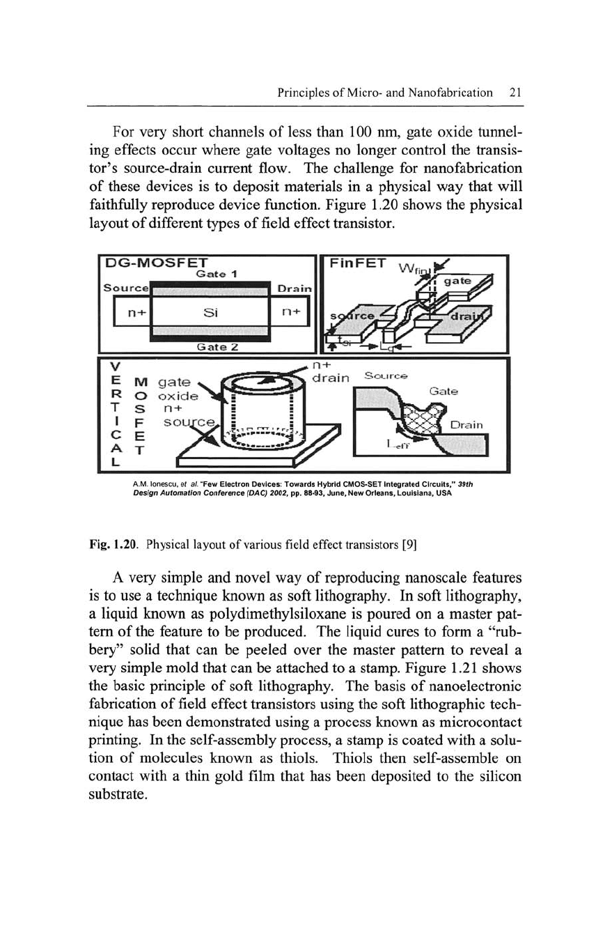
For very short channels of less than 100 nm, gate oxide tunnel-
ing effects occur where gate voltages no longer control the transis-
tor's source-drain current flow. The challenge for nanofabrication
of these devices is to deposit materials in a physical way that will
faithfully reproduce device function. Figure 1.20 shows the physical
layout of different types of field effect transistor.
DG-MOSFET
Gate 1
Sou rce^^^^^^^^^^^
RH
Si
Drain
nn
Gate 2
V
E M gate ^ t
R O oxide >f
T s n+ T
I F SOMTC^
Gate
Drain
A.M.
lonescu, et al. "Few Electron Devices: Towards Hybrid Ci\rtOS-SET Integrated Circuits," 39th
Design Automation Conference (DAC) 2002, pp. 88-93, June, New Orleans, Louisiana, USA
Fig. 1.20. Physical layout of various field effect transistors [9]
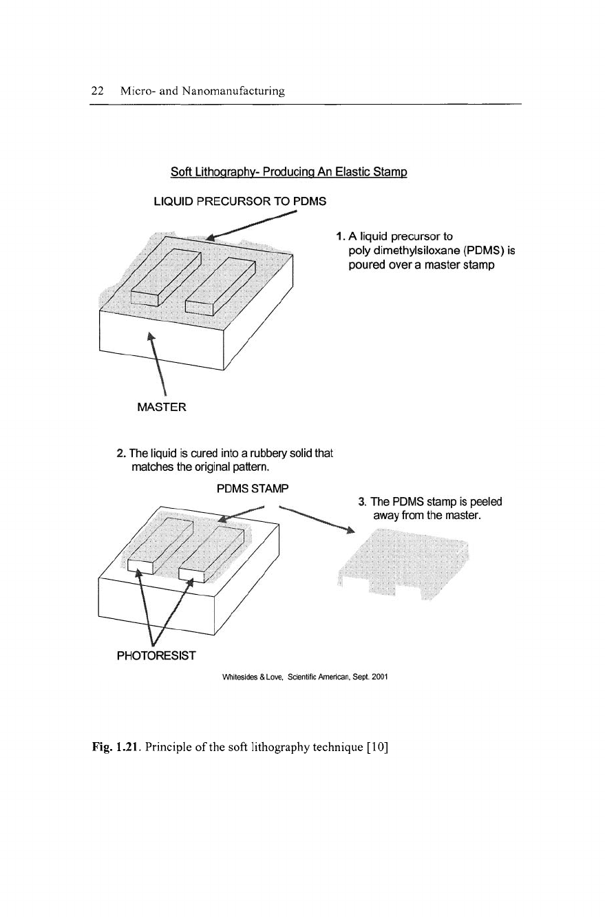
A very simple and novel way of reproducing nanoscale features
is to use a technique known as soft lithography. In soft lithography,
a liquid known as polydimethylsiloxane is poured on a master pat-
tern of the feature to be produced. The liquid cures to form a "rub-
bery" solid that can be peeled over the master pattern to reveal a
very simple mold that can be attached to a stamp. Figure 1.21 shows
the basic principle of soft lithography. The basis of nanoelectronic
fabrication of field effect transistors using the soft lithographic tech-
nique has been demonstrated using a process known as microcontact
printing. In the self-assembly process, a stamp is coated with a solu-
tion of molecules known as thiols. Thiols then self-assemble on
contact with a thin gold film that has been deposited to the silicon
substrate.
22 Micro- and Nanomanufacturing
Soft Lithography- Producing An Elastic Stamp
LIQUID PRECURSOR TO PDMS
1.
A liquid precursor to
poly dimethylsiloxane (PDMS) is
poured over a master stamp
MASTER
2.
The liquid is cured into
a
rubbery
solid
that
matches the original pattern.
PDMS STAMP
3. The
PDMS
stamp is peeled
away
from
the master.
PHOTORESIST
Whitesides & Love, Scientific American, Sept. 2001
Fig. 1.21. Principle of the soft lithography technique [10]
Principles of Micro- and Nanofabrication 23
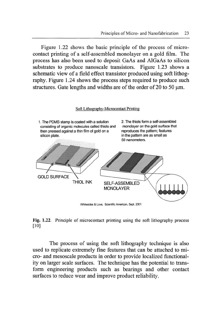
Figure 1.22 shows the basic principle of the process of micro-
contact printing of a self-assembled monolayer on a gold film. The
process has also been used to deposit GaAs and AlGaAs to silicon
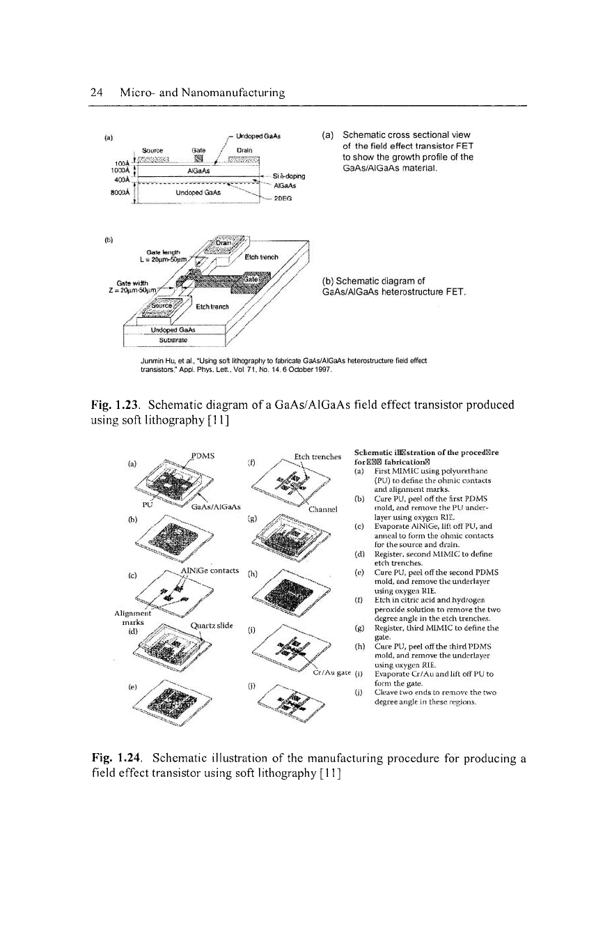
substrates to produce nanoscale transistors. Figure 1.23 shows a
schematic view of a field effect transistor produced using soft lithog-
raphy. Figure 1.24 shows the process steps required to produce such
structures. Gate lengths and widths are of the order of
20
to 50 |Lim.
Soft Lithographv-Microcontact Printing
1.
The PDMS stamp is coated with a solution
consisting of organic molecules called thiols and
then pressed against a thin film of gold on a
silicon plate.
2.
The thiols fomi a self-assembled
monolayer on the gold surface that
reproduces the pattern; features
in the pattern are as small as
50 nanometers.
GOLD SURFACE
THIOL INK
Whitesides & Love, Scientific American, Sept. 2001
Fig. 1.22. Principle of microcontact printing using the soft lithography process
[10]
The process of using the soft Hthography technique is also
used to replicate extremely fine features that can be attached to mi-
cro-
and mesoscale products in order to provide localized functional-
ity on larger scale surfaces. The technique has the potential to trans-
form engineering products such as bearings and other contact
surfaces to reduce wear and improve product reliability.
24 Micro- and Nanomanufacturing
IDOA
*Q>0A
J
400A
80v)0A
- Jt^<io{)ecl 6aAs
-JL
-* Si ivdopinq
*siGaAs
(a) Schematic cross sectional view
of the field effect transistor FET
to show the growth profile of the
GaAs/AIGaAs material.
Gale tentfth
(b) Schematic diagram of
GaAs/AIGaAs heterostructure FET.
SojrCR>'
)
EtchUnch
Sobslratc
Junmin Hu, et
al.,
"Using soft lithography to fabricate GaAs/AIGaAs heterostructure field effect
transistors," Appl. Phys. Lett., Vol.
71,
No. 14,
6
October 1997.
Fig. 1.23. Schematic diagram
of
a GaAs/AIGaAs field effect transistor produced
using soft lithography [11]
/ "^j^y
GaAs/AlGau\s
AlNiGr contacts
Quai
Iz
slide
(b)
^
/
Schematic illustration of the procedure
for ESS fabrication^
(a) Fir.st MIMIC using polyiirethane
(PU) to define the ohmic contacts
and alignment marks.
Cure PU, peel off the first PDM.S
mold, and remove the PU under-
layer using oxygen R.1E,
Evaporate AlNiGe, lift ofl PU, and
anneal to form the ohmic contacts
for
the source and drain.
Regi.ster, second MIMIC to define
etch trenches.
Cure PU, peel off the second PDMS
mold, and remove the underlayer
using oxygen PIE.
Etch in citric acid and hydrogen
perox-ide .solution
to
remove the two
degree angle in the etch trenches.
Register, third MIMIC to define the
gate.
Cure PU, peel off the third PDMS
mold, and remove the underlayer
using oxygen RIE.
Evaporate Cr/Au and lift
olT
PU
to
form the gate.
Cleave two ends to reitiove the two
degxee angle in these region.s.
Fig.
1.24.
Schematic illustration
of
the manufacturing procedure
for
producing
a
field effect transistor using soft lithography [11]
Principles of Micro- and Nanofabrication 25
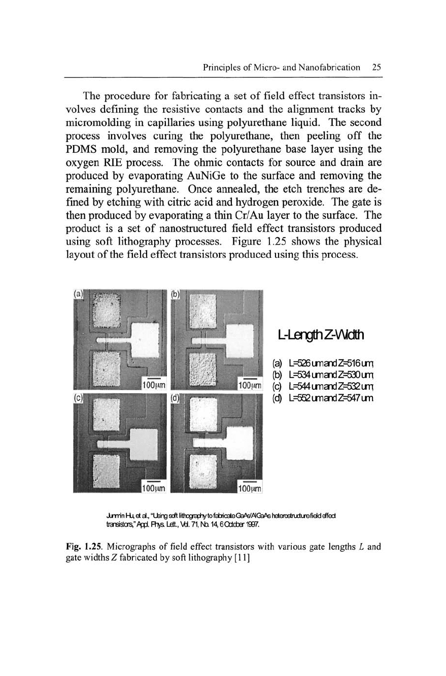
The procedure for fabricating a set of field effect transistors in-
volves defining the resistive contacts and the alignment tracks by
micromolding in capillaries using polyurethane liquid. The second
process involves curing the polyurethane, then peeling off the
PDMS mold, and removing the polyurethane base layer using the
oxygen RIE process. The ohmic contacts for source and drain are
produced by evaporating AuNiGe to the surface and removing the
remaining polyurethane. Once annealed, the etch trenches are de-
fined by etching with citric acid and hydrogen peroxide. The gate is
then produced by evaporating a thin Cr/Au layer to the surface. The
product is a set of nanostructured field effect transistors produced
using soft lithography processes. Figure 1.25 shows the physical
layout of the field effect transistors produced using this process.
1
m
Ip^j
F
\\ 1
,/•..- .,,
'.^^^g^
fi'Jfe)K-,;J •• .- -•
..'4$^
^11
• A
iilOOum
m
^^^m
PH^
U','-
.:
^
^^^H
; _ . •
llOOum
L-LergthZ-Wdth
(a) L=526LjnandZ=516LJT;
(b) L=534umaxlZ=630LrTi
lOOiun
(c)
L=544umandZ=^32Lin
(cO L=^562umaxlZ=647Lm
JLmin
Hu,
et
al.,
"Ufeing
scft lithogaftyto
fabricate
QBMAIQB/^
hetercstruiLiie
field
effect
transistcrs,"
Aip(i.
Fhya Lett.,
VDI.
71,
ISh 14,6 Otcber 1997.
Fig. 1.25. Micrographs of field effect transistors with various gate lengths L and
gate widths Z fabricated by soft lithography [11]

26 Micro- and Nanomanufacturing
The fabrication of nanoelectronic features using soft lithography
is at an early stage but promises to overcome the limitations experi-
enced using optical methods of lithography, such as overcoming the
diffraction limit observed in photolithography.
ScaiiiingRiobeMGnosoqy
Seaming Timding McroGcq?/
(SI^^
(BhiTJg t^nr, 1982)
Aicmc Fcnoe Mcroscofy
(AFN^
^nFblari2DdSTlVI nP-FfenUthcgraphy
QBdAMridnetal.
_AFMTip_
Saeme283,661
ritolecutar transport
Seti^Asseiifclcd
Soiid Substrate
Fig. 1.26. Manipulative techniques used for nanofabrication
Nanofabrication Using Manipulative Techniques
Nanofabrication using manipulative techniques is a promising way
of producing nano-based electronic components using processes
such as scanning tunneling microscopy, atomic force microscopy,
spin-polarized scanning tunneling microscopy, and dip pen nano-
lithography. Figure 1.26 shows the difference between these ma-
nipulative techniques. Scanning tunneling microscopy is a process
that relies on a very sharp tip connected to a cantilever beam to
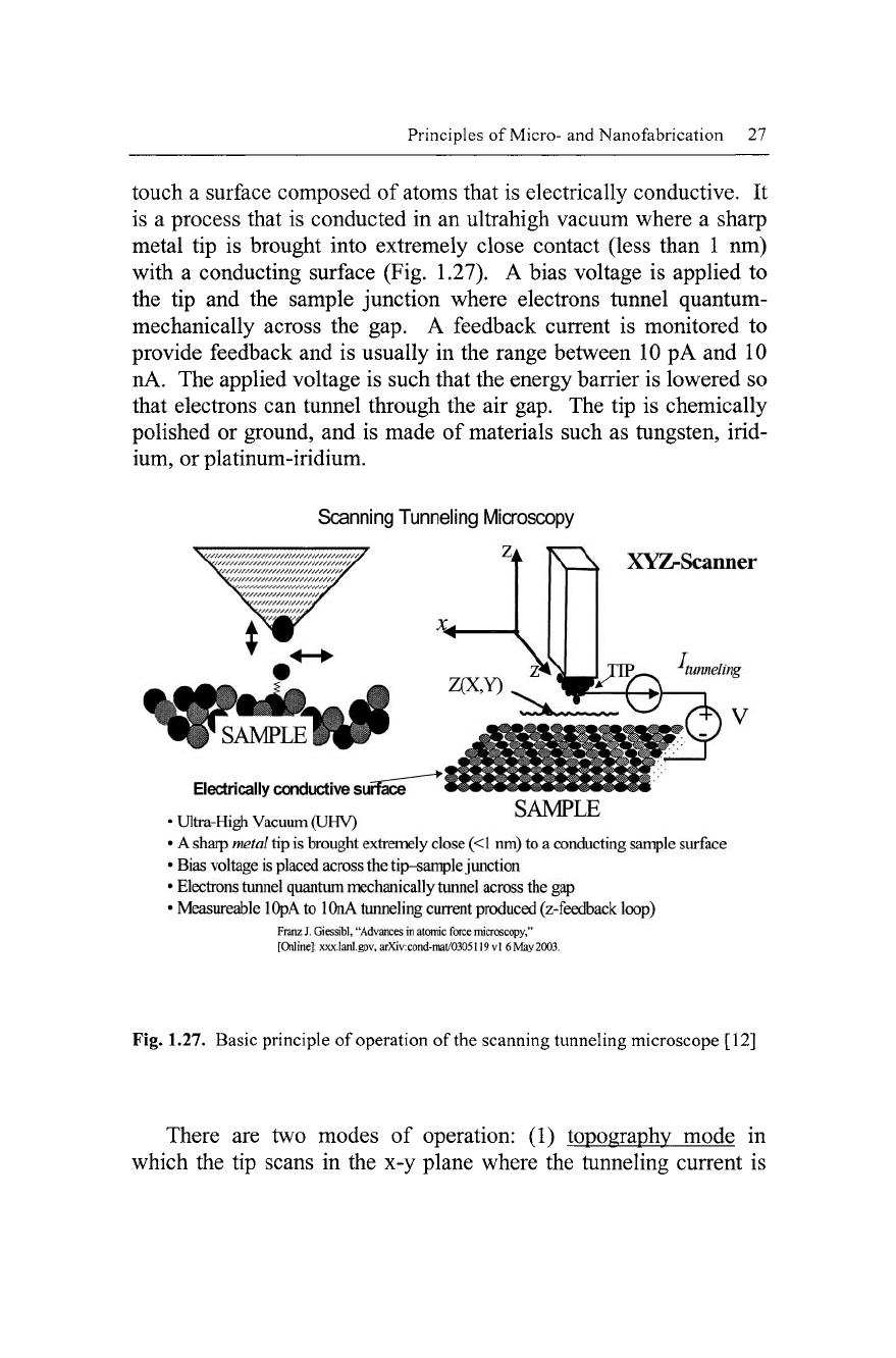
Principles of Micro- and Nanofabrication 27
touch
a
surface composed
of
atoms that
is
electrically conductive.
It
is
a
process that
is
conducted
in an
ultrahigh vacuum where
a
sharp
metal
tip is
brought into extremely close contact (less than
1 nm)
with
a
conducting surface (Fig.
1.27).
A
bias voltage
is
applied
to
the
tip and the
sample junction where electrons tunnel quantum-
mechanically across
the gap. A
feedback current
is
monitored
to
provide feedback
and is
usually
in the
range between 10
pA and 10
nA. The applied voltage
is
such that the energy barrier
is
lowered
so
that electrons
can
tunnel through
the air
gap.
The tip is
chemically
polished
or
ground,
and is
made
of
materials such
as
tungsten, irid-
ium, or platinum-iridium.
Scanning Tunneling Microscopy
XYZ^Scanner
Electrically conductive surface
• Ultra-High Vacuum (UHV)
•
A
sharp metal tip is brought extremely close
(<1
nm)
to a
conducting sample surface
• Bias voltage is placed across the tip-sanple junction
• Electrons tunnel quantum mechanically tunnel across the gap
• Measureable lOpA to lOnA tunneling current produced (z-feedback loop)
Franz J. Giessibl, "Advances
in
atomic force microscopy,"
[Online]:
xxx.lanl.gov, arXiv:cond-mat/0305119
vl 6
May
2003.
Fig. 1.27. Basic principle of operation of the scanning tunneling microscope [12]
There
are two
modes
of
operation:
(1)
topography mode
in
which
the tip
scans
in the x-y
plane where
the
tunneling current
is
28 Micro- and Nanomanufacturing
kept constant and; (2) constant height mode where the tip is scanned
in the x-y plane at constant depth and the tunneUng current is modu-
lated.
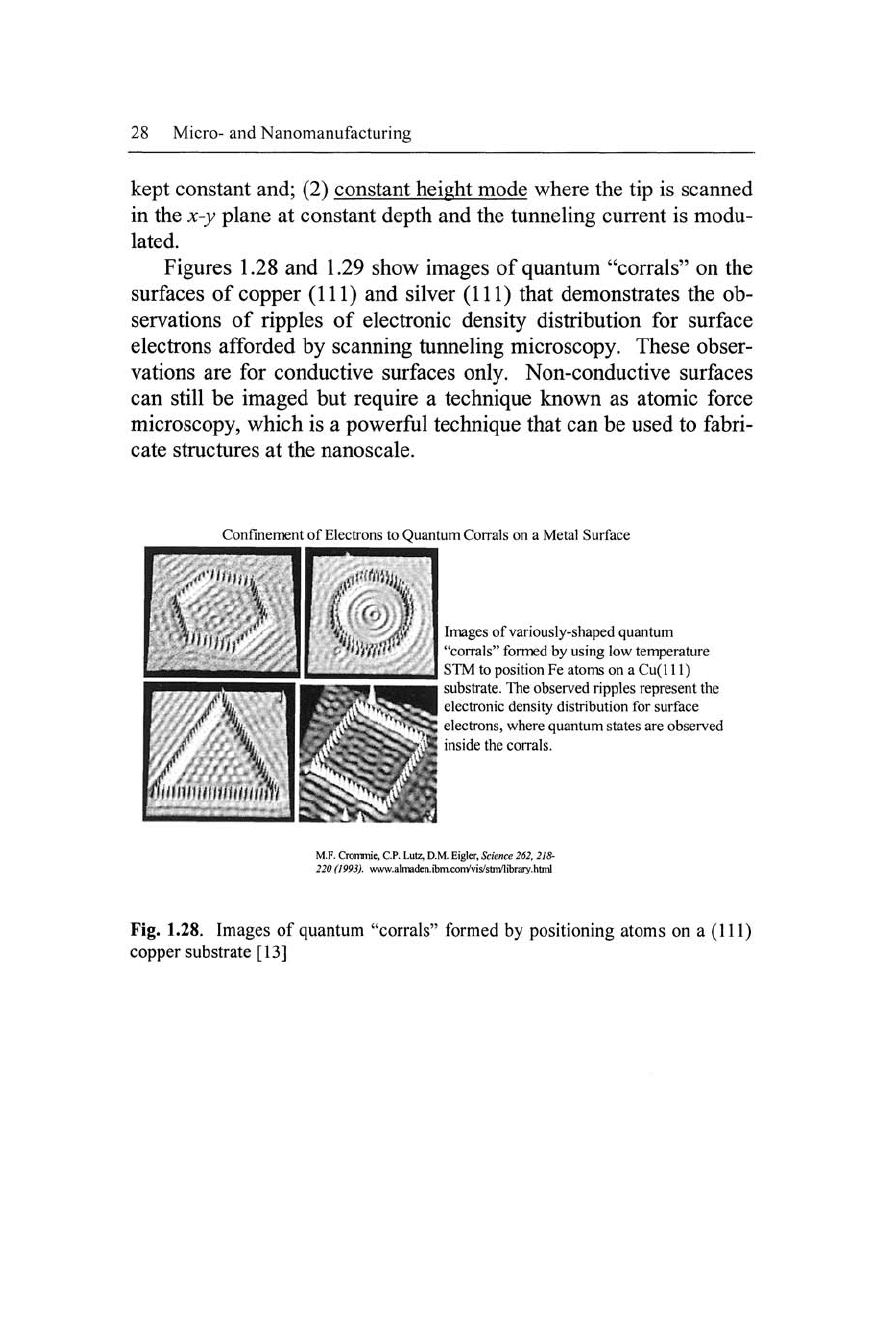
Figures 1.28 and 1.29 show images of quantum "corrals" on the
surfaces of copper (111) and silver (111) that demonstrates the ob-
servations of ripples of electronic density distribution for surface
electrons afforded by scanning tunneling microscopy. These obser-
vations are for conductive surfaces only. Non-conductive surfaces
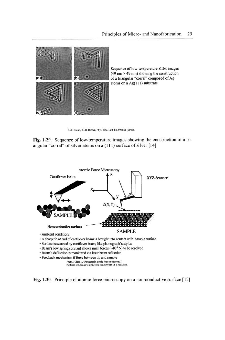
can still be imaged but require a technique known as atomic force
microscopy, which is a powerful technique that can be used to fabri-
cate structures at the nanoscale.
Confinement of Electrons to Quantum Corrals on a Metal Surface
•:XJ^''^^U)
'iL'
wmmmmm
Images of variously-shaped quantum
"corrals" formed by using low temperature
STM to position Fe atoms on a Cu(l 11)
substrate. The observed ripples represent the
electronic density distribution for surface
r^^^ electrons, where quantum states are observed
inside the corrals.
M.F. Crommie, C.P. Lutz, D.M. Eigler, Science 262. 218-
220 (1993). www.almaden.ibnxconyvis/stm'library.html
Fig. 1.28. Images of quantum "corrals" formed by positioning atoms on a (111)
copper substrate [13]
Principles
of
Micro-
and
Nanofabrication
29
Sequence
of
low-temperature STM images
(49 nm
x
49 nm) showing the construction
of
a
triangular "corral" composed of
Ag
atoms on
a
Ag(l 11) substrate.
K.-F.
Braun, K.-H. Rieder, Phys. Rev. Lett. 88, 096801 (2002).
Fig. 1.29. Sequence of low-temperature images showing the construction of a tri-
angular "corral" of silver atoms on a (111) surface of silver [14]
Atomic Force Microscopy
Cantilever
beam
XYZ-Scaimer
Nonconductive surface
SAMPLE
• Ambient conditions
•
A
sharp tip at end of cantilever beam is brought into contact with sample surface
• Surface is scanned by cantilever beam, like phonograph's stylus
• Beam's low spring constant allows small forces (-10-^ N) to be resolved
• Beam's deflection is monitored via laser beam reflection
• Feedback mechanism
if
force between tip and sample
Franz
J.
Giessibl, "Advances in atomic force microscopy,"
[Online]:
xxx.lanl.gov, arXiv:cond-niat/0305119 vl 6 May
2003.
Fig. 1.30. Principle of atomic force microscopy on a non-conductive surface [12]
30 Micro- and Nanomanufacturing
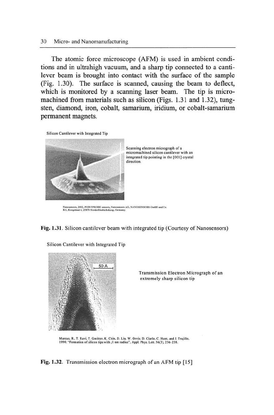
The atomic force microscope (AFM) is used in ambient condi-
tions and in ultrahigh vacuum, and a sharp tip connected to a canti-
lever beam is brought into contact with the surface of the sample
(Fig.
1.30).
The surface is scanned, causing the beam to deflect,
which is monitored by a scanning laser beam. The tip is micro-
machined from materials such as silicon (Figs. 1.31 and
1.32),
tung-
sten, diamond, iron, cobalt, samarium, iridium, or cobalt-samarium
permanent magnets.
Silicon Cantilever with Integrated Tip
Scanning electron micrograph of a
micromachined silicon cantilever with an
integrated tip pointing in the [001] crystal
direction.
Fig. 1.31. Silicon cantilever beam with integrated tip (Courtesy of Nanosensors)
Silicon Cantilever with Integrated Tip
50 A •
Transmission Electron Micrograph of an
extremely sharp silicon tip
Marcus, R., T. Ravi, T. Gniitter, K. Chin, D. Liu, W. Orvis, D. Ciarlo, C. Hunt, and J. Trujillo,
1990,
"Formation of silicon tips with jl nm radius", Appl. Phys. Lett. 56(3), 236-238.
Fig. 1.32. Transmission electron micrograph of an AFM tip [15]