Jackson M.J. Micro and Nanomanufacturing
Подождите немного. Документ загружается.

1.
Principles of IVIicro- and Nanofabrication
1.1 Introduction
Innovations in the area of micro and nanofabrication have created
opportunities to manufacture structures at the nanometer and milli-
meter scales. These opportunities can be used to fabricate elec-
tronic, optical, magnetic, and chemical/biological devices ranging
from sensors to computation and control systems. In this chapter,
we introduce the dominant micro and nanofabrication techniques
that are currently used to fabricate structures in the nanometer scale
up to the millimeter scale. The first part of this chapter focuses on
microfabrication of MEMS and semiconductor devices as an exam-
ple of microfabrication. Next, the chapter focuses on nanofabrica-
tion techniques including several top-down and bottom-up tech-
niques. Again, we use semiconductor devices as an example that
shows the promising techniques that can be used to manufacture
nanofabricated structures.
Most micro and nanofabrication techniques were developed
by the semiconductor industry. The semiconductor industry has
grown rapidly in the past 30 years, which is driven by the microelec-
tronics revolution. The desire to place many transistors on to a sili-
con wafer has demanded innovative ways to fabricate electronic cir-
cuits and to fit more and more electronic devices into a smaller
workable area. Early transistors were made from germanium but are
now predominantly silicon, with the remainder made from gallium
arsenide. While gallium arsenide has high electron mobility com-
pared to silicon, it has low hole mobility, a poor thermal oxide, less
stability during thermal processing, and much higher defect density
than silicon. Silicon is the material of choice for most electronic ap-
plication but gallium arsenide is useful for circuits that operate at
high speeds with low-to-moderate levels of integration. This type of
2 Micro- and Nanomanufacturing
material is used for analog circuits operating at speeds in excess of
10^
Hz. The performance of integrated circuits can be increased by
placing transistors closer together and by depositing transistors in a
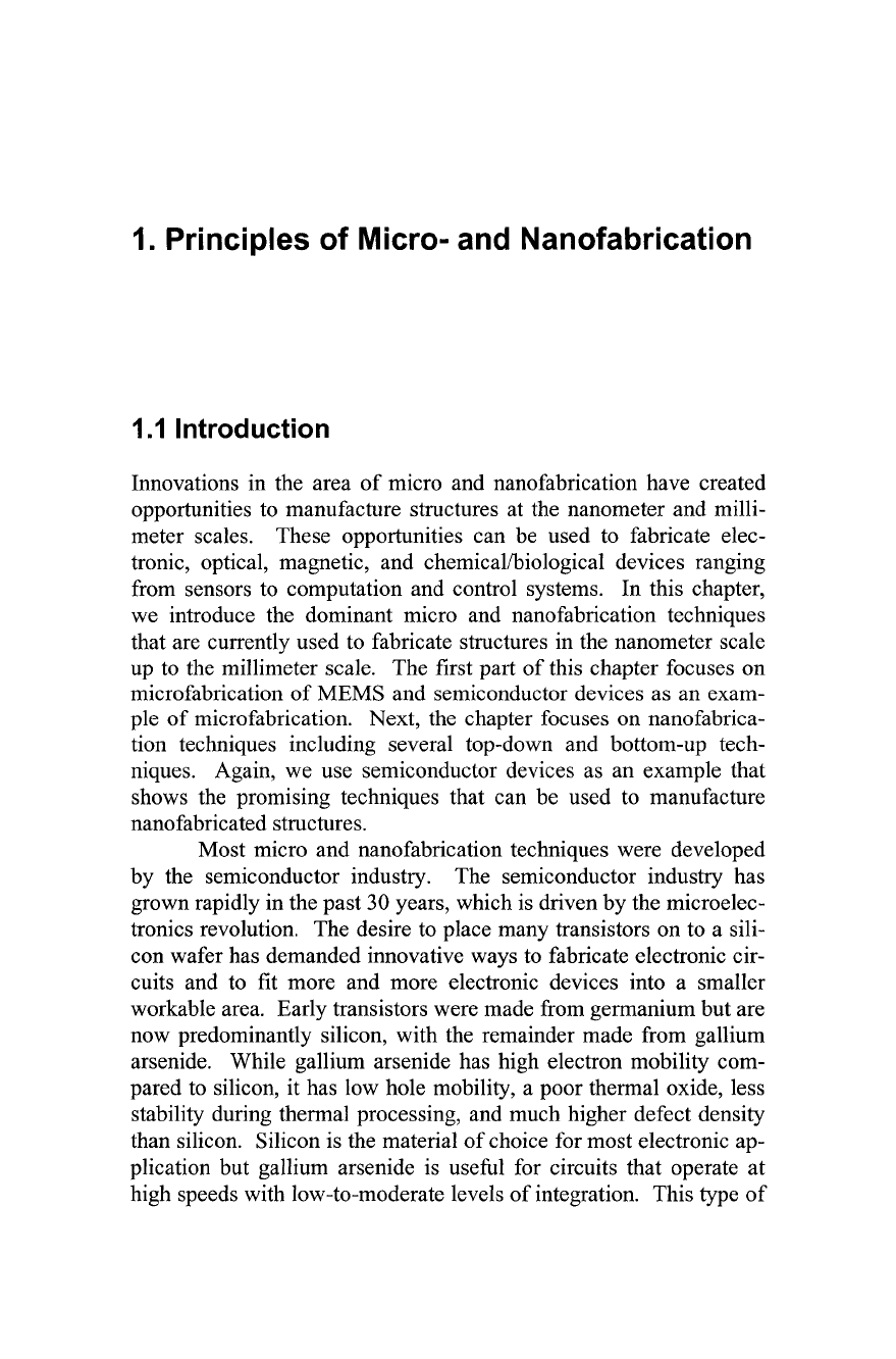
precise way. The minimum feature size has reduced at an astonish-
ing rate over the past thirty years. Figure 1.1 shows the reduction in
the feature sizes as a function of the number of transistors per chip
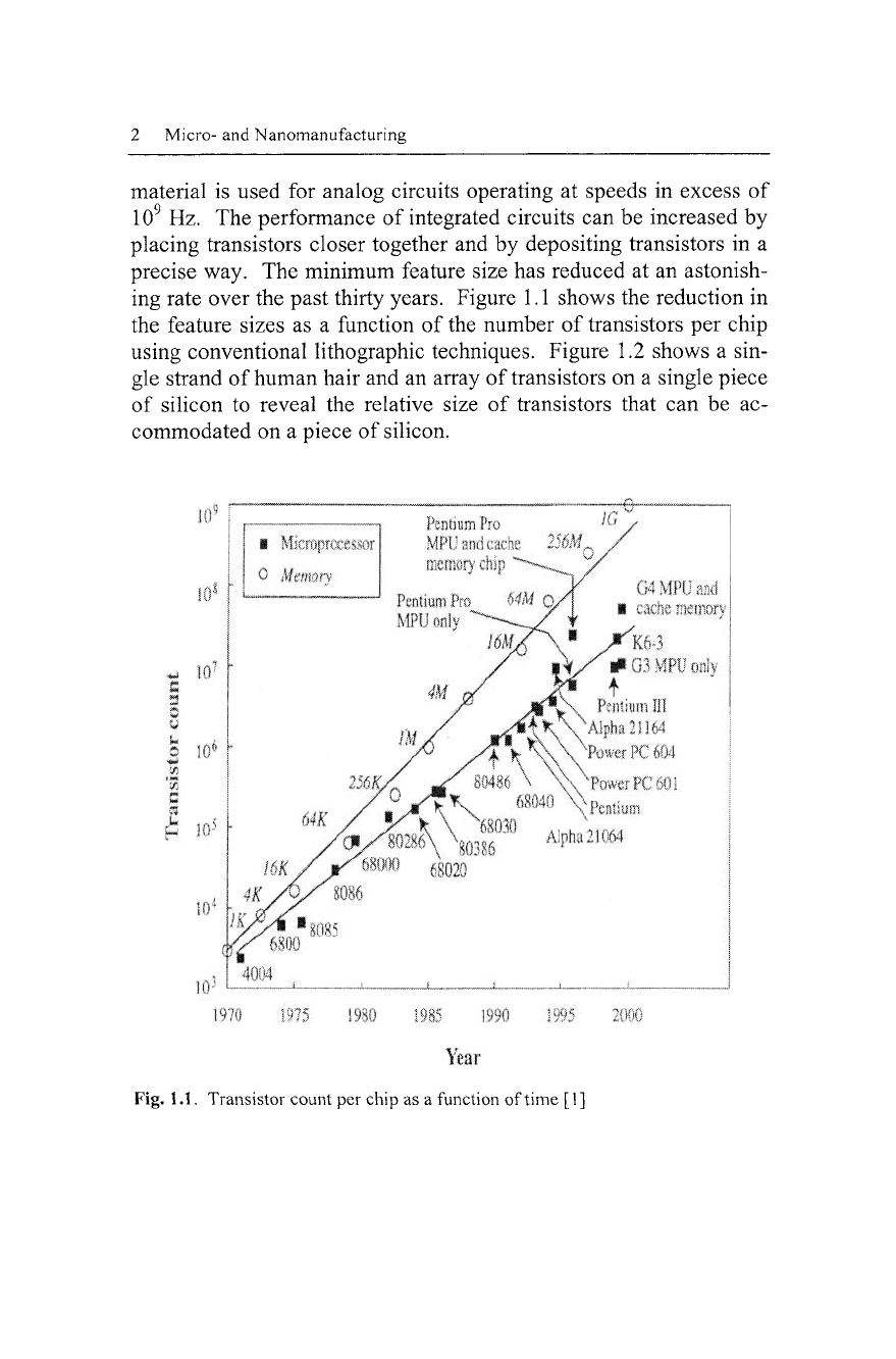
using conventional lithographic techniques. Figure 1.2 shows a sin-
gle strand of human hair and an array of transistors on a single piece
of silicon to reveal the relative size of transistors that can be ac-
commodated on a piece of silicon.
V^ln
'^^Hy r-M!) ;^/K5 r'90 :?^^5
Year
Fig. 1.1. Transistor count per chip as a function of time [1]
Principles of Micro- and Nanofabrication 3
Fig. 1.2. Scanning electron micrograph of an integrated circuit chip in the mid-
1980s. The human hair to the left of the image provides an indication of the rela-
tive size of the transistor wires [1]
Microfabrication begins when a set of photomasks are provided to
the integrated circuit fabricator. The photomasks are physical repre-
sentations of the design of the circuits to be manufactured in accor-
dance with the rules of layout. A silicon wafer provides the basis of
the integrated circuit. Wafers are processed using a grinding process
that produces a flat surface that is still conductive at this stage. The
wafer is insulated by growing a thermal oxide layer so that leakage
of current between transistors is prevented. A conducting layer is
deposited that will be used for producing transistors. Several tech-
niques have been developed for depositing insulating and conduct-
ing layers such as sputtering, physical vapor deposition using a
magnetron, chemical vapor deposition (CVD), and epitaxial growth
of layers using techniques such as metal oxide CVD, molecular
beam epitaxy, and chemical beam epitaxy. The conducting layer is
divided up into individual resistors. Individual resistors are depos-
ited to the wafer using photolithographic techniques. Further proc-
essing is required that forms the integrated circuit and uses tech-
niques such as pattern transfer, etching, deposition, and growth.
These same techniques have also been used to create a plethora of
microscale products in silicon-based materials for applications other
than integrated circuits.
4 Micro-
and
Nanomanufacturing
1.1.1 Microfabrication
of
MEMS and Semiconductor Devices
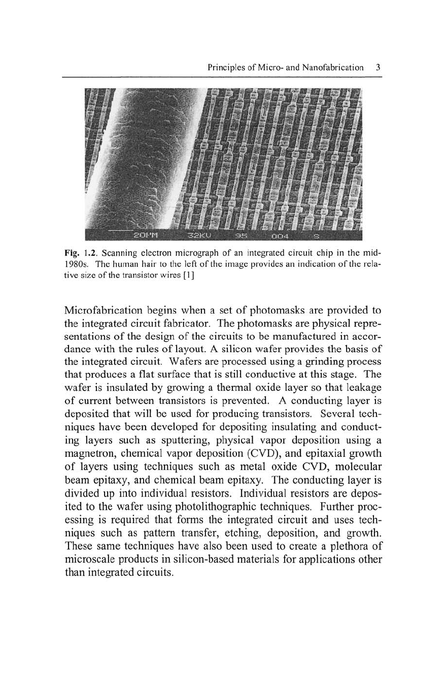
Traditionally, integrated circuits have been manufactured using
mi-
crofabrication techniques that have been classified
as
machining
processes. Figure
1.3
shows
the
standard route followed
to
produce
an integrated circuit.
The
same flowchart can be used
for
producing
any microscale product produced using silicon-based materials.
The
chart shows
the
basic functions that are composed
of
initially clean-
ing
the
substrate, applying
a
thin film using many deposition tech-
niques, applying lithographic techniques
to
apply mask material,
etching
to
form
the
required shape
of
the
microscale features,
re-
moval
of
the mask material using chemical
or
plasma etching, then
finally characterizing
the
nature
of
the created structure.
The
final
microstructures
are
then separated from
the
initial subtrate material
and released
for
quality control.
Standard Mcromachining Flow
Substrate
Qean
Repeat
oJ
rumseum
"^ Apply thin filixi'~'^^'^y'^^p°^^^^°"*^^^"^
Lithograph
Wet,
plasma,
etc.
-
i
-Etch
i
Qean
Apply masking material
•Expose
to
pattem
•
Develq)
•
Cure masking material
Inspect
Remove mask
materiah—chemicai orpiasma
I Qean
Characterization
Mcroscopy,
electrical,
I
adhesion,
etc.
Release/Separate
Fig.
1.3.
Standard micromachining flow chart showing various processing steps
Principles of Micro- and Nanofabrication 5
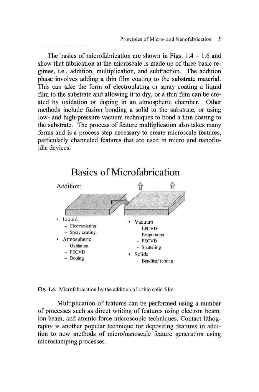
The basics of microfabrication are shown in Figs. 1.4 - 1.6 and
show that fabrication at the microscale is made up of three basic re-
gimes, i.e., addition, multiplication, and subtraction. The addition
phase involves adding a thin film coating to the substrate material.
This can take the form of electroplating or spray coating a liquid
film to the substrate and allowing it to dry, or a thin film can be cre-
ated by oxidation or doping in an atmospheric chamber. Other
methods include fusion bonding a solid to the substrate, or using
low- and high-pressure vacuum techniques to bond a thin coating to
the substrate. The process of feature multiplication also takes many
forms and is a process step necessary to create microscale features,
particularly channeled features that are used in micro and nanoflu-
idic devices.
Basics of Microfabrication
Liquid
- Electroplating
- Spray coating
Atmospheric
- Oxidation
- PECVD
- Doping
Vacuum
- LPCVD
- Evaporation
- PECVD
- sputtering
Solids
- Bonding/joining
Fig. 1.4. Microfabrication by the addition of
a
thin solid film
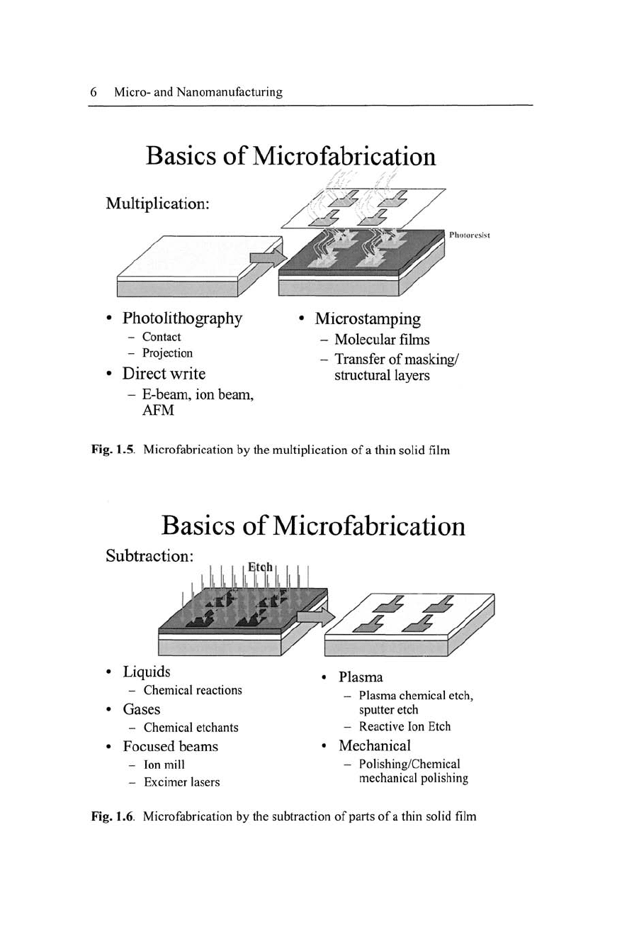
Multiplication of features can be performed using a number
of processes such as direct writing of features using electron beam,
ion beam, and atomic force microscopic techniques. Contact lithog-
raphy is another popular technique for depositing features in addi-
tion to new methods of micro/nanoscale feature generation using
microstamping processes.
6 Micro- and Nanomanufacturing
Basics of Microfabrication
Multiplication
~~^ nintorv.sisi
Photolithography
- Contact
- Projection
Direct write
- E-beam, ion beam,
AFM
Microstamping
- Molecular films
- Transfer of masking/
structural layers
Fig. 1.5. Microfabrication by the multiplication of a thin solid film
Basics of Microfabrication
Subtraction:
III
ii mil
111
I
Liquids
- Chemical reactions
Gases
- Chemical etchants
Focused beams
- Ion mill
- Excimer lasers
^ ^
^ ^
Plasma
- Plasma chemical etch,
sputter etch
- Reactive Ion Etch
Mechanical
- Polishing/Chemical
mechanical polishing
Fig. 1.6. Microfabrication by the subtraction of parts of
a
thin solid film
Principles of Micro- and Nanofabrication
Subtraction of material to create features can be performed using a
variety of techniques shown in Fig. 1.6. In materials other than sili-
con, subtraction processes can include mechanical micromilling, la-
ser ablation, water micromachining, and a great number of other
processes. These processes can remove material at much higher ma-
terial removal rates and are discussed further in subsequent chapters
in this textbook. Combinations of all of these techniques can be used
to produce features of different size, shape, and scale. The standard
way of creating features on single pieces of silicon is being sur-
passed by new microfabrication processes that achieve improved
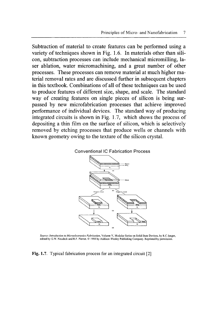
performance of individual devices. The standard way of producing
integrated circuits is shown in Fig. 1.7, which shows the process of
depositing a thin film on the surface of siHcon, which is selectively
removed by etching processes that produce wells or channels with
known geometry owing to the texture of the silicon crystal.
Conventional IC Fabrication Process
Source: Introduction to Microelectronics Fabrication, Volume V, Modular Series on Solid State Devices, by R.C Jaeger,
edited by G.W. Neudeck and R.F. Pierret. © 1988 by Addison-Wesley Publishing Company. Reprinted by permission.
Fig. 1.7. TjqDical fabrication process for an integrated circuit [2]
8 Micro- and Nanomanufacturing
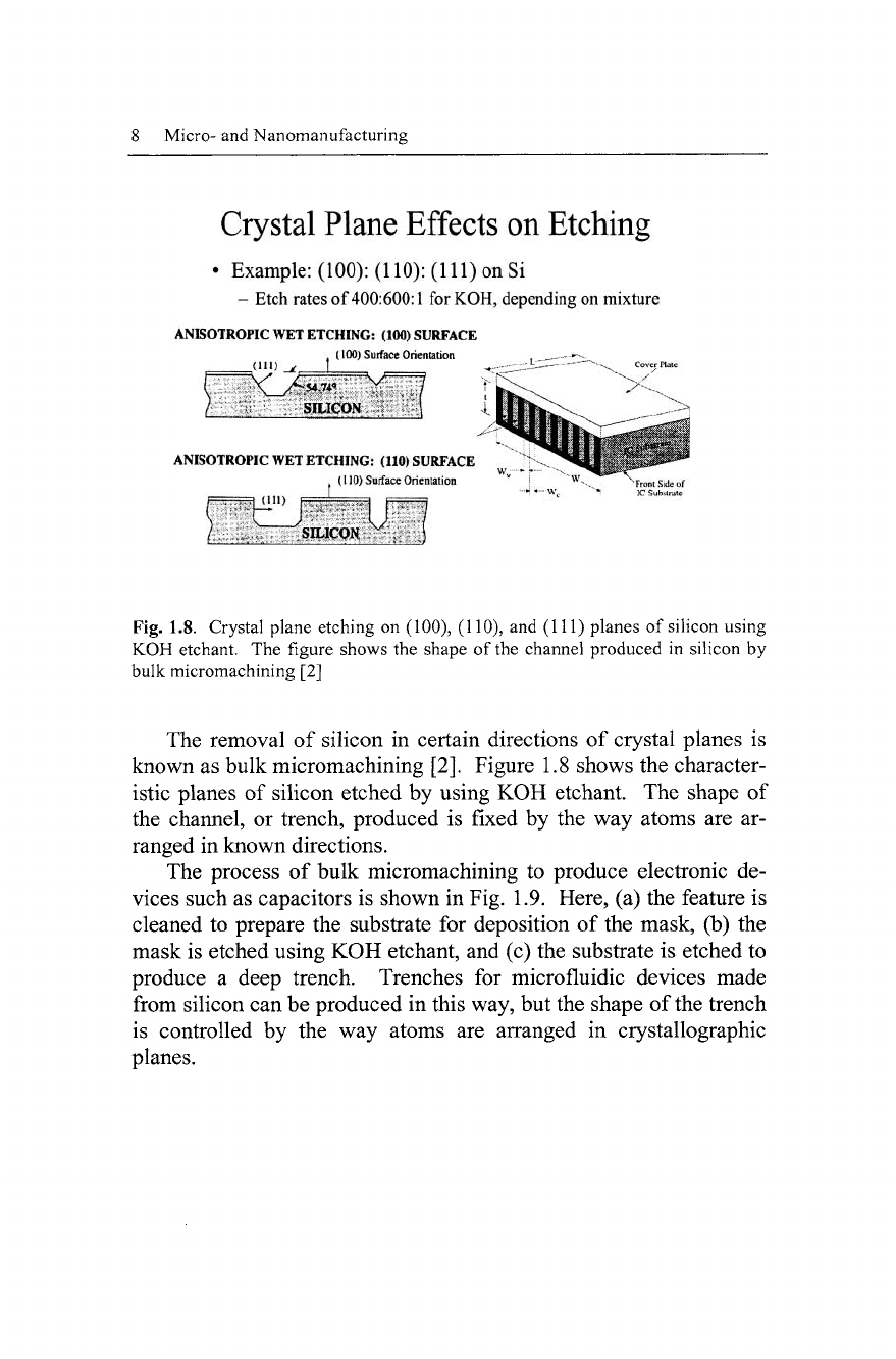
Crystal Plane Effects on Etching
• Example: (100): (110): (111) on Si
- Etch rates of 400:600:1 for KOH, depending on mixture
ANISOTROPIC WET ETCHING: (100) SURFACE
(100) Surface Orientation
^Kj'^^^nrz.
siacoN. :
ANISOTROPIC WET
ETCHING:
(110) SURFACE
(110) Surface Orientation
(111)
Fig. 1.8. Crystal plane etching on (100), (110), and (111) planes of silicon using
KOH etchant. The figure shows the shape of the channel produced in silicon by
bulk micromachining [2]
The removal of silicon in certain directions of crystal planes is
known as bulk micromachining [2]. Figure 1.8 shows the character-
istic planes of silicon etched by using KOH etchant. The shape of
the channel, or trench, produced is fixed by the way atoms are ar-
ranged in known directions.
The process of bulk micromachining to produce electronic de-
vices such as capacitors is shown in Fig. 1.9. Here, (a) the feature is
cleaned to prepare the substrate for deposition of the mask, (b) the
mask is etched using KOH etchant, and (c) the substrate is etched to
produce a deep trench. Trenches for microfluidic devices made
from silicon can be produced in this way, but the shape of the trench
is controlled by the way atoms are arranged in crystallographic
planes.
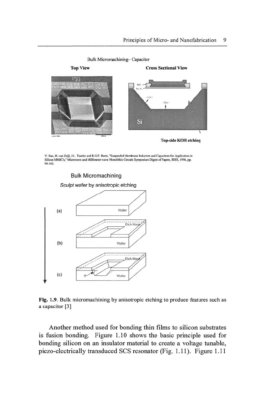
Principles of Micro- and Nanofabrication 9
Bulk Micromachining- Capacitor
Top View Cross Sectional View
Top-side KOH etching
Y. Sun, H. van Zeijl, J.L. Tauritz and R.G.F. Baets, "Suspended Membrane Inductors and Capacitors for Application in
Silicon MMICs," MiCTOwave and Millimeter-wave Monolithic Circuits Symposium Digest of Papers, IEEE, 1996, pp.
99-102.
Bulk Micromachining
Sculpt
wafer by anisotropic etching
(a)
(b)
(c)
Fig. 1.9. Bulk micromachining by anisotropic etching to produce features such as
a capacitor [3]
Another method used for bonding thin films to sihcon substrates
is fusion bonding. Figure 1.10 shows the basic principle used for
bonding silicon on an insulator material to create a voltage tunable,
piezo-electrically transduced SCS resonator (Fig.
1.11).
Figure 1.11
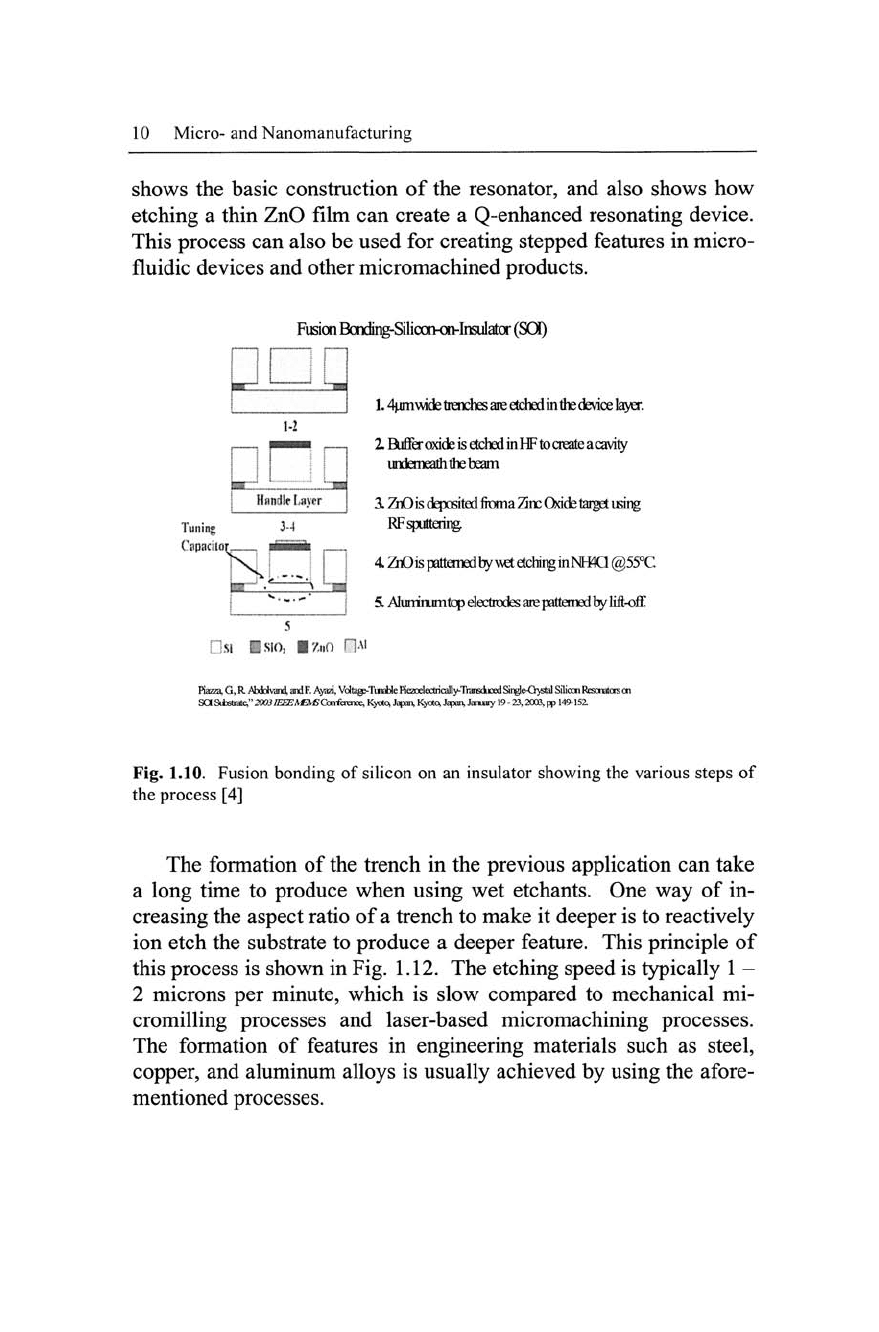
10 Micro-and Nanomanufacturing
shows
the
basic construction
of
the resonator,
and
also shows
how
etching
a
thin ZnO film
can
create
a
Q-enhanced resonating device.
This process can also
be
used
for
creating stepped features
in
micro-
fluidic devices and other micromachined products.
Fusion Bording-Silicon-m-Iiisulator (SQ)
1-2
HfiRdlf Lavcr
Tuning
CspscilO]
3-4
fSSmk
[—
\
LM
*^. .•. ^'
1.4|jmwide
trendies are etdied in the device la^.
1 Buffer oxide
is
etd^d in HF to create a cavity
undaneathflie beam
3.
ZiO
is
dqxKited
fiona Znc Odde target using
RF^xittair^
4 ZnOispattanedby wetetchii^inNBia @55°C
5 Aluninumtq) electrodes are pattoned by lift-off
DM
IsiOi
l/no n-\f
Piazza, G,
R
Abdalvand,
andF.
Ayazi,
Vdtagp-TuiaHeRezoelecrically-TransdicedSii^e-Q>stal SilicmResonators
a
Sa
Siistrate,"
2003 IEEE A^MCcxrfeKnx,
Kyoto,
Japan,
Kyoto,
Japan,
January
19 -
23,2CXB,
pp 149-152
Fig. 1.10. Fusion bonding of silicon on an insulator showing the various steps of
the process [4]
The formation
of
the trench
in the
previous application
can
take
a long time
to
produce when using
wet
etchants.
One way of in-
creasing the aspect ratio
of
a trench
to
make
it
deeper is
to
reactively
ion etch the substrate
to
produce
a
deeper feature. This principle
of
this process
is
shown
in
Fig.
1.12.
The etching speed
is
typically
1
-
2 microns
per
minute, which
is
slow compared
to
mechanical
mi-
cromilling processes
and
laser-based micromachining processes.
The formation
of
features
in
engineering materials such
as
steel,
copper, and aluminum alloys
is
usually achieved
by
using the afore-
mentioned processes.