Jackson M.J. Micro and Nanomanufacturing
Подождите немного. Документ загружается.

Micro- and Nanomanufacturing 643
^K
»
i'*t *
i * •»! *f
i *^ ( ^i *
* '* f '» i ^(
I
*,l u*
*^ 1 U * **
16.0
liO
3
1
i
(£
w
^*
'#
f 1.0
«^
335&
™
2S1 29?
^
5
*
1
U iillli
61M
iili
/ [f \ _J I'
^'
t,
we
BJ9 Mj m mi ^"
r«jK) /
/m
'"•w
i
!/•
•x 1
210
"-I
162
79
1
1
1
i
i"
IVt
ik-LJ
u..,„-^'
[
J
i
11
U-'.
|105?
i
)
i
j!
I|
i
1
;=
!:
h^,^
l»
100 iSi m 5,50
TiTClminl
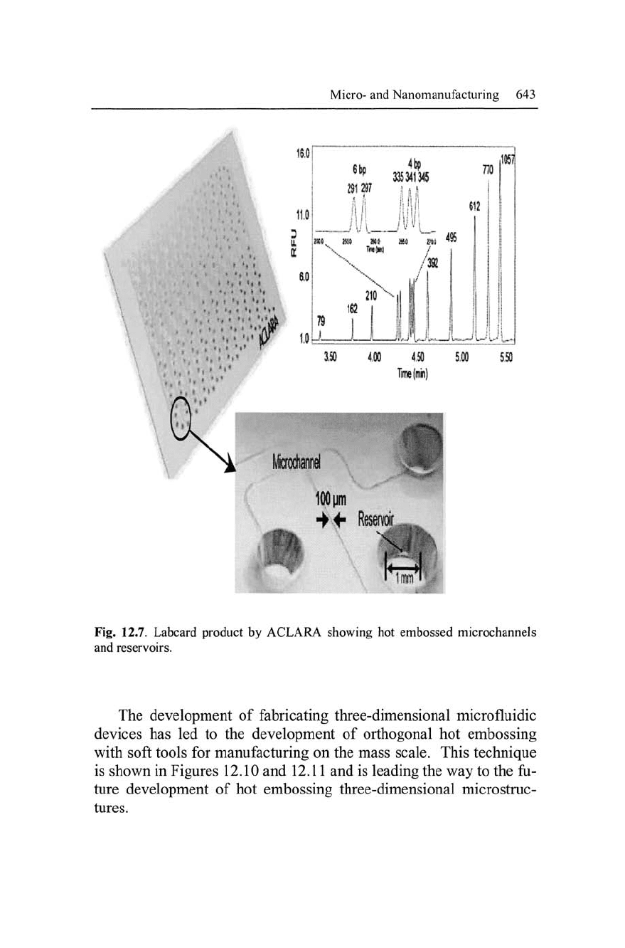
Fig. 12.7. Labcard product by ACLARA showing hot embossed microchannels
and reservoirs.
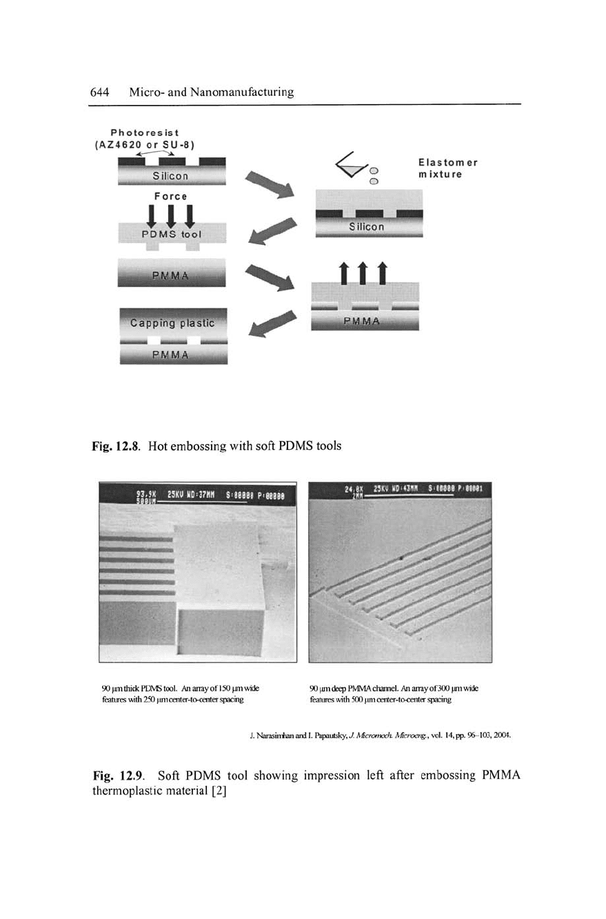
The development of fabricating three-dimensional microfluidic
devices has led to the development of orthogonal hot embossing
with soft tools for manufacturing on the mass scale. This technique
is shown in Figures 12.10 and 12.11 and is leading the way to the fu-
ture development of hot embossing three-dimensional microstruc-
tures.
644 Micro- and Nanomanufacturing
Photoresist
(AZ4620
or
SU-8)
Silicon
Force
PDMS tool
<^,
Elastom
er
m ixture
Silicon
ttt
Fig.
12.8. Hot embossing with soft PDMS tools
?3>9»{
tm
i}D:37HR $:e8aee P'^eaBe
zi.n
»xu HD^oitn
s^m«9
?
tmi
90 jjiii thick
PDIVB
tool.
An array of
150
loiiiwide
features with
250
)jni center-to-center spacing
90 |jm deep PMMA channel. An array of 300 pni wide
features with 500 ^ni center-to-centCT spacing
J. Narasimhan and
I.
Papautsky,
J.
Mcromeck
Mcroeng.,
vol.
14, pp.
96-103,2004.
Fig.
12.9. Soft PDMS tool showing impression left after embossing PMMA
thermoplastic material [2]
Micro- and Nanomanufacturing 645
AZ4620 SU-8
Silicon
Force
PDMS Tool
T^mwiwc
^J^^
Elastomer
mixture
tn
'""PIWySBJP'
Twwr
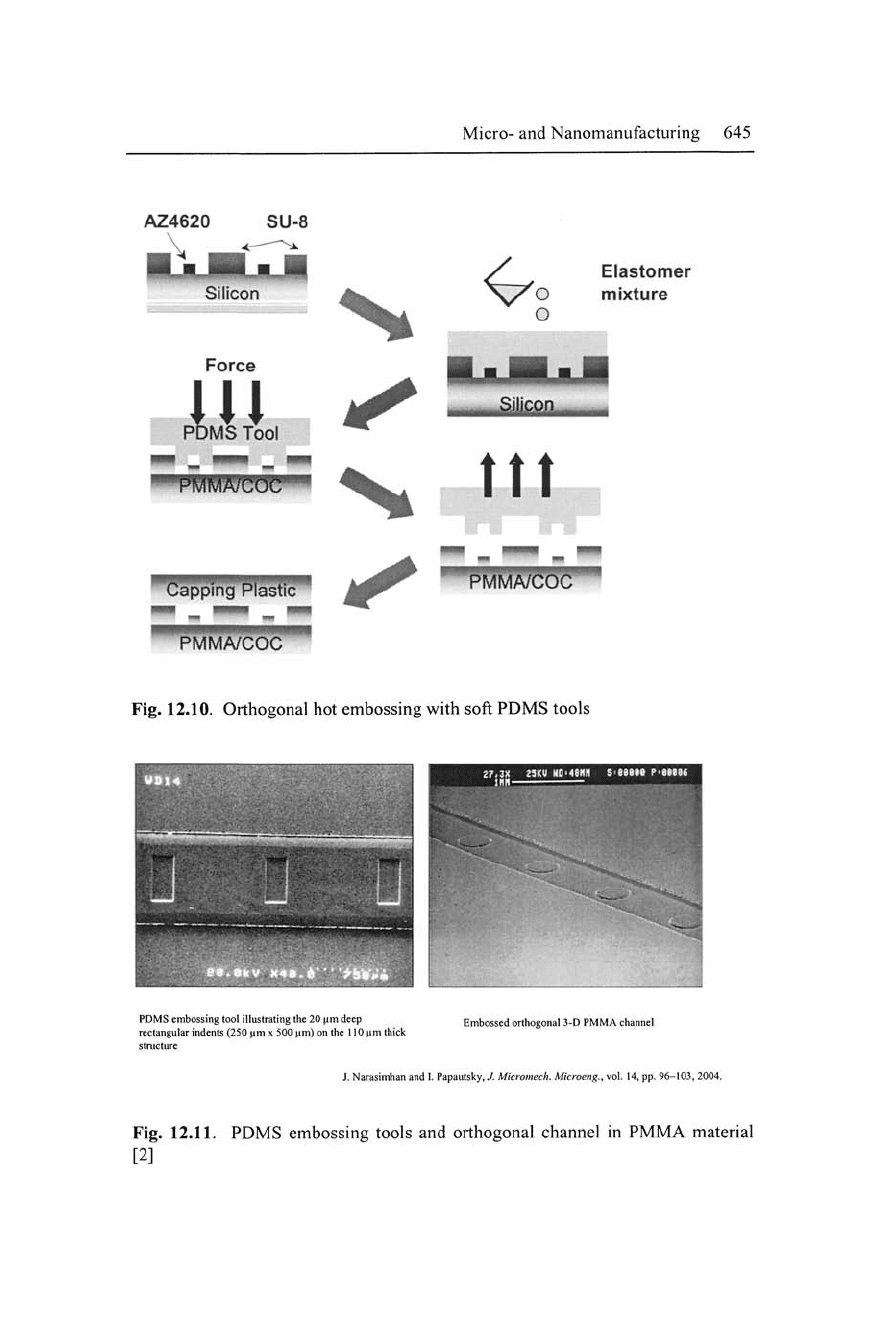
Fig. 12.10. Orthogonal hot embossing with soft PDMS tools
PDMS embossing tool illustrating the 20 |im deep
rectangular indents (250
jxm
x 500 |im) on the 110 ^m thick
structure
Embossed orthogonal 3-D PMMA channel
J. Narasimhan and I. Papautsky,
J.
Micromech.
Microeng.,
vol.
14,
pp. 96-103, 2004.
Fig.
12.11.
PDMS embossing tools and orthogonal channel in PMMA material
[2]
646 Micro- and Nanomanufacturing
The critical issue for the future development of micromolding
techniques such as hot embossing with soft tools is concerned with
the faithful replication of the master pattern during hot embossing,
which requires the application of a uniform force for the appropriate
cycle time on the tool-polymer sandwich. This criterion in turn re-
quires the embossing tool to be uniform in thickness throughout,
which is achieved by casting on a highly flat and leveled hot plate.
The embossing parameters are different from those normally used
with Ni or Si tools, in part due to a much lower thermal conductivity
of PDMS (^0.2 W/mK) compared with Ni (--150 - 500 W/mK) or Si
(157 W/mK) and the soft nature of the tool iself The lifetime of soft
tools have also been determined to last approximately twenty mold-
ings with aspect ratios between 2 and 4, creating a minimum feature
size of about
10
// m. The use of soft tools and polymers looks set to
open up future opportunities for creating all polymer transistors, cir-
cuits,
and microprocessors.
12.2.4 Machining
The process of machining has always been a strong contender for
playing a role in the future of micromanufacturing. The ability to
machine any material guarantees that micromachining will continue
to be a micromanufacturing process of choice. In recent years, the
size of the cutting tool has become smaller and smaller, and as such
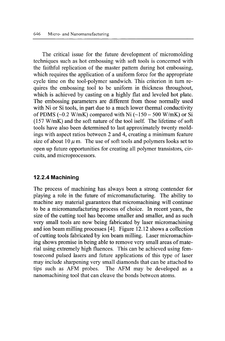
very small tools are now being fabricated by laser micromachining
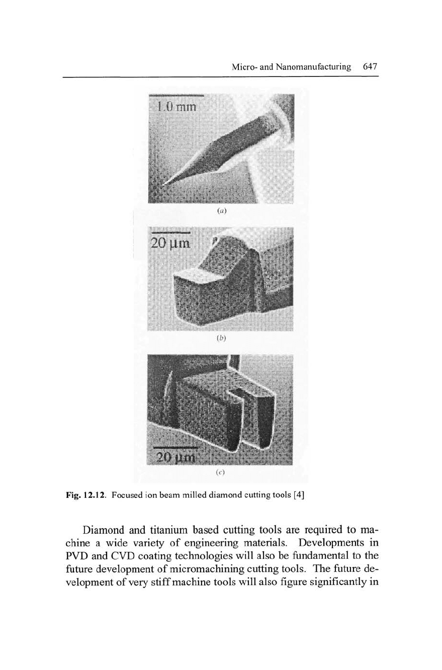
and ion beam milling processes [4]. Figure 12.12 shows a collection
of cutting tools fabricated by ion beam milling. Laser micromachin-
ing shows promise in being able to remove very small areas of mate-
rial using extremely high fluences. This can be achieved using fem-
tosecond pulsed lasers and future applications of this type of laser
may include sharpening very small diamonds that can be attached to
tips such as AFM probes. The AFM may be developed as a
nanomachining tool that can cleave the bonds between atoms.
Micro- and Nanomanufacturing 647
20
\xm
••3*^"
1:2teM^^8fic:%-^v^
Fig. 12.12. Focused ion beam milled diamond cutting tools [4]
Diamond and titanium based cutting tools are required to ma-
chine a wide variety of engineering materials. Developments in
PVD and CVD coating technologies will also be fundamental to the
future development of micromachining cutting tools. The future de-
velopment of very stiff machine tools will also figure significantly in
648 Micro- and Nanomanufacturing
the future too. Developments in this area have already begun by
various research institutions in the United States and are described
as "meso-micro machine tools" (mMTs).
12.2.5 Future Developments in Micromanufacturing
The development of micromanufacturing processes that use silicon-
based materials are already highly developed. The next stage in the
development of micromanufacturing processes lies in the ability to
manufacture micro-products from engineering materials such as
metals and ceramics. Processes that show promise in promoting the
next stage of development include selective laser sintering of metals,
laser micromachining using pulsed femto- and attosecond lasers,
droplet-based manufacturing, and cold gas dynamic molding and
spraying of microparts. Combinations of these techniques and es-
tablished methods of manufacturing that produce hybrid manufactur-
ing processes will create the short term "stepping stones" required to
meet the demand generated to economically manufacture microscale
products.
12.3 Nanomanufacturing
12.3.1 Semiconductor IVIanufacturing
Semiconductor manufacturers have made great strides in the past
few years overcoming the diffraction limit of light waves to produce
nanoscale transistors. The scale of engineering the limit to favor the
semiconductor industry involves the use of extreme ultra violet light
sources and soft "x-rays". However, the use of photolithographic
processes to produce transistors at length scales of the order of tens
of nanometers will be reached within the next 5 years. Alternative
manufacturing methods are required to produce features sizes in the
range of tens of nanometers. A number of processes are emerging
from universities and research institutes that will form the basis of
future nanomanufacturing processes. The following descriptions of
Micro- and Nanomanufacturing 649
processes form the basis of the future direction of nanomanufactur-
ing.
12.3.2 Soft Lithographic IVIanufacturing
Soft lithographic processes are currently being developed for nano-
manufacturing of semiconductor and non-semiconductor applica-
tions and include techniques such as microcontact printing (mini-
mum feature size of 35 nm), replica molding (minimum feature size
of 30 nm), microtransfer molding (minimum feature size of 500
nm),
micromolding in capillaries (minimum feature size of 350 nm),
and solvent assisted micromolding (minimum feature size of 60 nm)
amongst others. Micro-contact printing is a non-photolithographic
method that routinely forms patterned self assembled monolayers.
An elastic stamp made from PDMS is used to transfer inks of mole-
cules or colloids of nanoparticles to the surface of the substrate be-
ing printed. The process can be made into a "manufacturing" proc-
ess by adding a roller to form a rolling stamp. Figure 12.13 shows
the principle of the process. Contact times of less than 30ms are re-
quired to deposit molecules to the surface of the substrate making
microcontact printing a relatively fast process. Deposition on the
surface of silver appears to be better than gold owing to silver's re-
activity to etchants and its high electrical conductivity. Multilayers
possess fewer defects than gold layers and edge distortions are less
because the deposited layers are 1 - 3 nm in thickness. PDMS
stamp require rigid backings so that the stamp does not lose form
during printing. The development of higher quality elastomers may
be necessary although reinforcing existing elastomers such as Syl-
gard 184 with metal particles may be the answer. The patterning of
non-planar surfaces is possible with this mechanical form of hthog-
raphy compared to the optical techniques. The development of mi-
crocontact printing as a nanomanufacturing process depends on the
ability to deposit a variety of materials. So far, organic molecules
and colloids of metals such as palladium have been successfully de-
posited. Future development of this process lies in the deposition of
materials to substrates other than silicon and glass.
650 Micro- and Nanomanufacturing
A)
PGMS
""5 ^/^'^^'A
?"''*''5
V"'"f V""/ '<•'
c>
Fig.
12.13.
Schematic diagram of microcontact printing of self-assembled
monlayers (hexadecanethiol, HDT) to a gold surface: (a) printing a planar surface
with a planar stamp; (b) large area planar printing with a rolling stamp; and (c)
printing on a non-planar surface with a planar stamp [5]
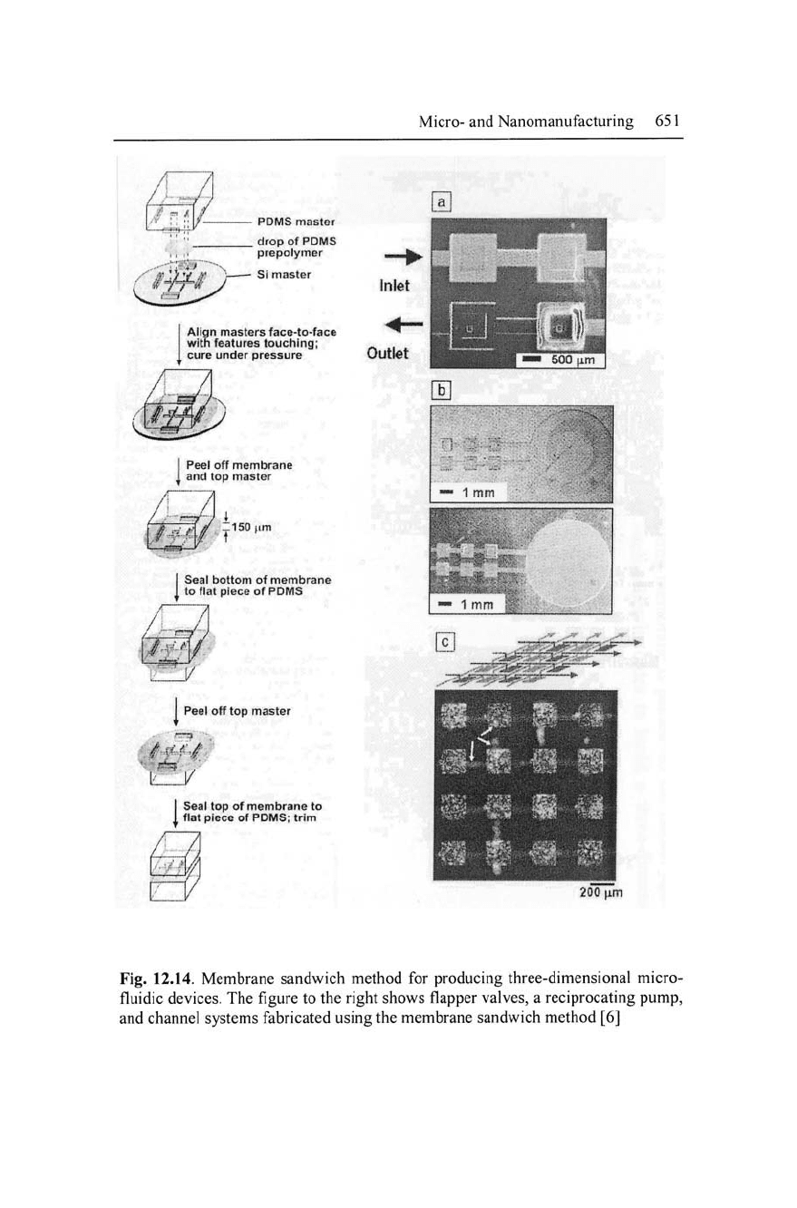
Microcontact printing can also be performed to produce three-
dimensional structures such as microfluidic devices using the sand-
wich method of printing. A PDMS master stamp is coated with a
drop of PDMS pre-polymer which is stamped against the master pat-
tern of a silicon substrate. Masters are aligned with features just
touching where the PDMS pre-polymer cures under pressure. The
resulting membrane is peeled off the master and can be laid on top
of each other in order to build a three-dimensional device (Fig.
12.14).
Micro- and Nanomanufacturing 651
/j^f\
PDMS master
dropof PDMS
prepolyinor
Si master
Align masters face-to-facD
with features touching;
cure under pressure
Peel off membrane
and top master
150 nm
Seal bottom of membrane
flat piece of PDMS
Peel off top master
k 1/
I
Seal top of membrane to
flat piece of PDMS; trim
Inlet
Outlet
200 fim
Fig. 12.14. Membrane sandwich method for producing three-dimensional micro-
fluidic devices. The figure to the right shows flapper valves, a reciprocating pump,
and channel systems fabricated using the membrane sandwich method [6]
652 Micro- and Nanomanufacturing
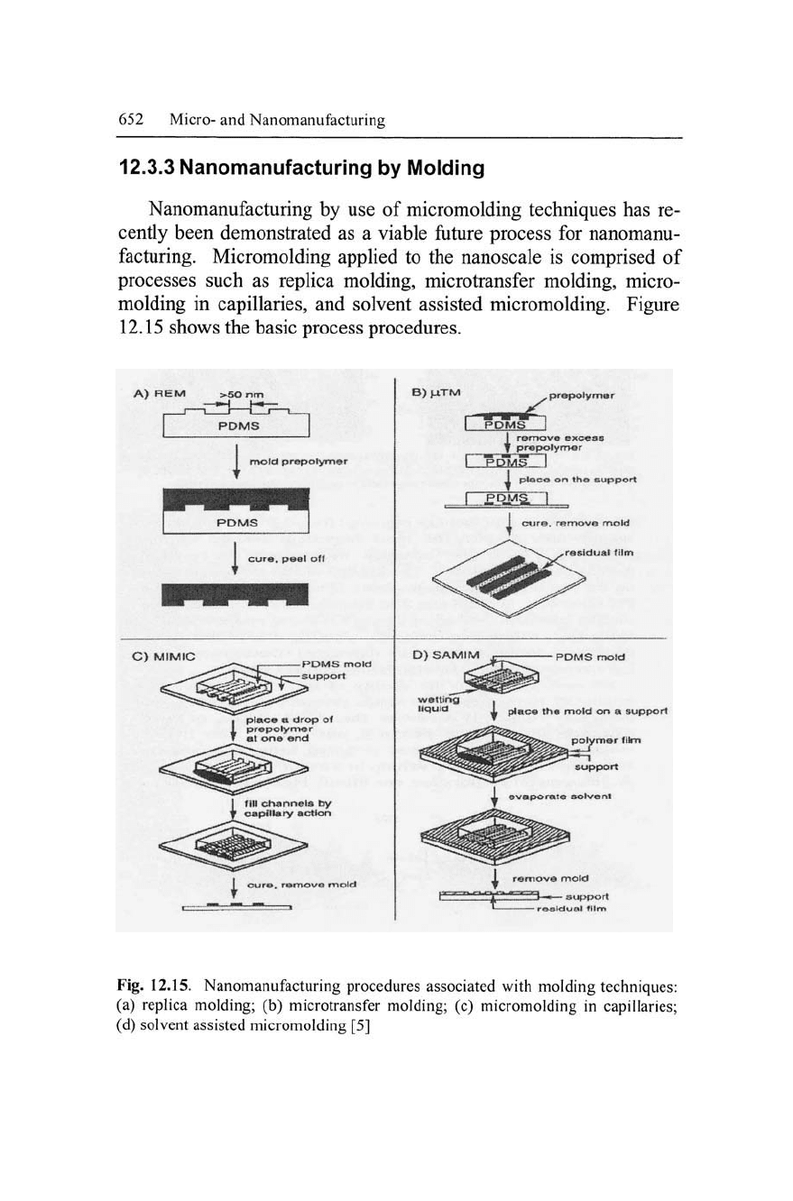
12.3.3 Nanomanufacturing by Molding
Nanomanufacturing by use of micromolding techniques has re-
cently been demonstrated as a viable future process for nanomanu-
facturing. Micromolding applied to the nanoscale is comprised of
processes such as replica molding, microtransfer molding, micro-
molding in capillaries, and solvent assisted micromolding. Figure
12.15 shows the basic process procedures.
mold prepolymer
cure, peal oU
S)UTM
propotymer
romovo exc«ss
pre polymer
ptaco on tho support
A^
crijre.
remove mold
rasiduai tiim
C) MIMIC
place a drop of
prepolymer
at one end
PDMS mold
support
D) SAMIM
- PDMS mold
waning .
liquid I pj^ce the mold on a support
fill clionneis by
capillary action
cure,
remove moid
residual film
Fig. 12.15. Nanomanufacturing procedures associated with molding techniques:
(a) repHca molding; (b) microtransfer molding; (c) micromolding in capillaries;
(d) solvent assisted micromolding [5]