Jackson M.J. Micro and Nanomanufacturing
Подождите немного. Документ загружается.

462 Micro- and Nanomanufacturing
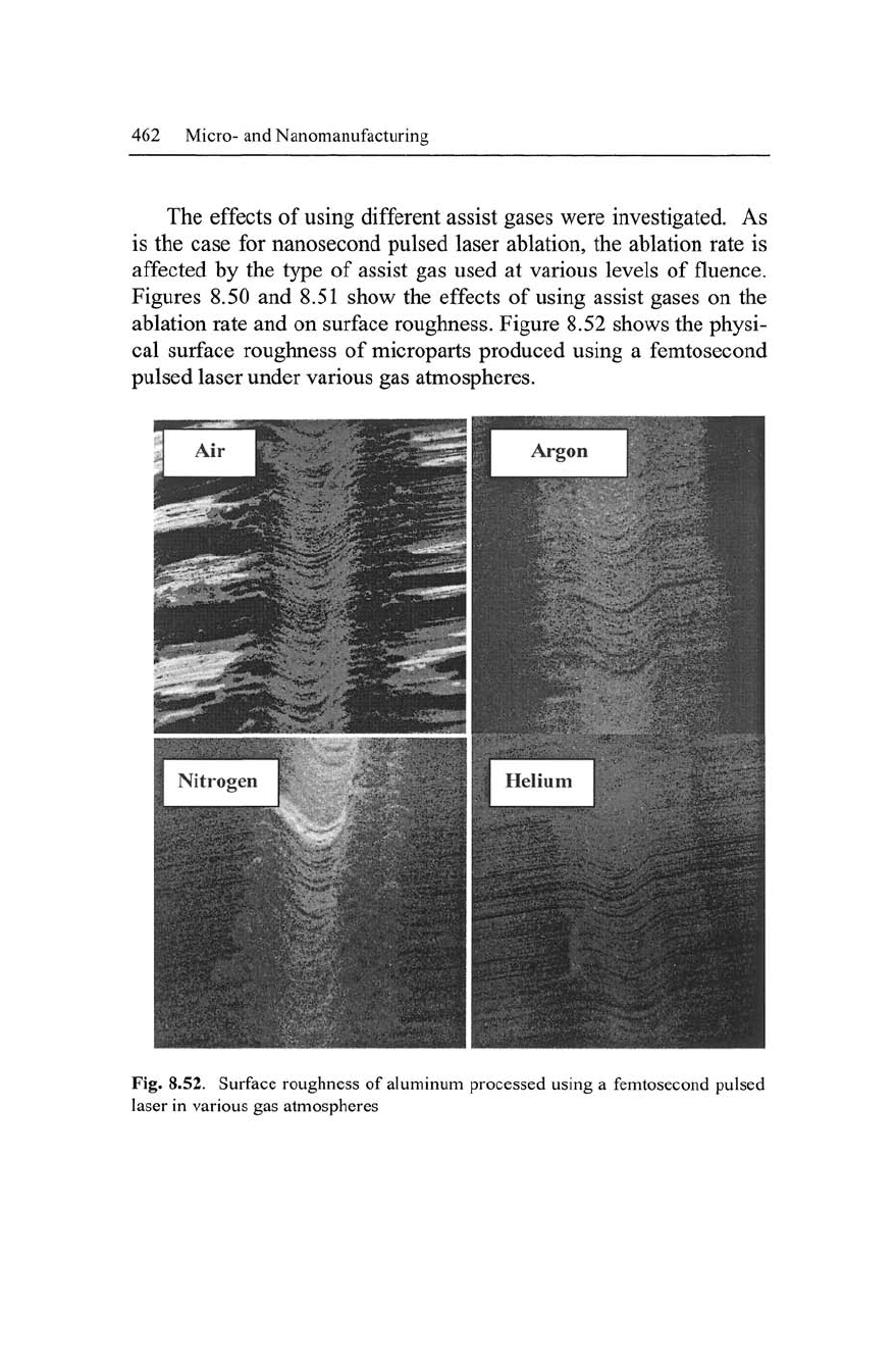
The effects of using different assist gases were investigated. As
is the case for nanosecond pulsed laser ablation, the ablation rate is
affected by the type of assist gas used at various levels of fluence.
Figures 8.50 and 8.51 show the effects of using assist gases on the
ablation rate and on surface roughness. Figure 8.52 shows the physi-
cal surface roughness of microparts produced using a femtosecond
pulsed laser under various gas atmospheres.
Fig. 8.52. Surface roughness of aluminum processed using a femtosecond pulsed
laser in various gas atmospheres
Laser Micro- and Nanofabrication 463
Note that the roughness of the machined trenches is identical to
the roughness of the original material. This is because the femtosec-
ond laser removes a very small amount of material. Thus the same
vertical distance is removed and an identical profile to that at the
surface is created at the base and side walls of the trench. Air pro-
duces relatively good results with small amounts build-up of mate-
rial around the edges. Argon produces a powdery residue around the
track, while nitrogen yields poor results, causing a build-up of mate-
rial around the machined trench or channel. Helium produced the
cleanest results. All other gases produced a powder that was black,
helium on the other hand, produced a silvery deposit. The black
powder produced was thought to be a nanoscale powder with depos-
its so small they are below the wavelength of light and therefore no
interaction is possible, resulting in the black appearance. Clearly the
assist gas has some effect but this has not yet been quantified. Proc-
essing with femtosecond lasers may provide an economic way to
produce nanometal powders.
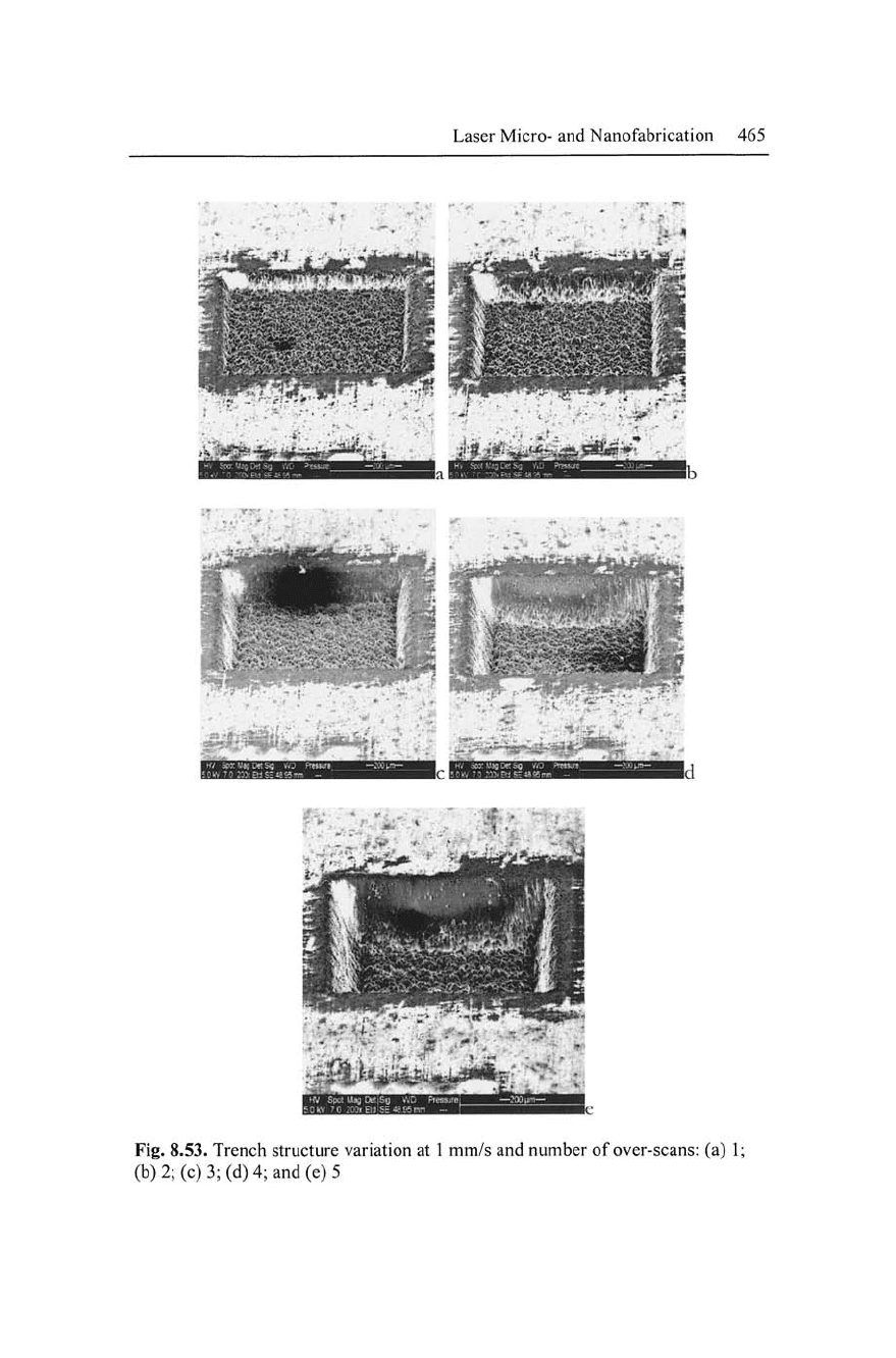
8.3.9 Effects of Femtosecond Laser Machining
The following results are conducted in an ambient airflow generated
at 150 |LJ/pulse, the spot diameter is approximately 30 |Lim and is
slightly elliptical the overlap between lines is 10 |Lim. The results in
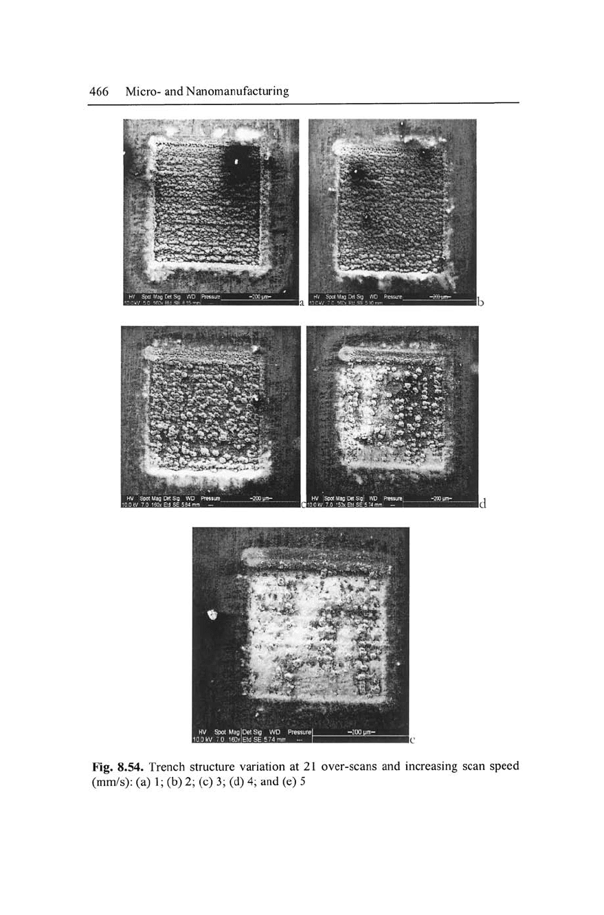
Figure 8.53 show the effect of increasing the number of over-scans
in aluminium while maintaining the laser power and scan speed. The
textured surface produced at the base of the cube increases in vari-
ability with increasing number of
scans.
It can be seen, that the relief
of the sidewalls, becomes more severe as the number of over-scans
increases; this may be attributed to the nature and shape of the Gaus-
sian profile of the beam.
The textured surface appears to be globules of metal left behind
by ablation of the surrounding matrix. Alternatively, the structured
surface could be condensed droplets of re-cast that have fallen and
solidified. Alternatively, the texture could be localized solidified
melt pools created by the heat from the plasma (heat from the beam
directly evaporates material, therefore, if present, secondary heating
effects are likely to arise from the plasma). Figure 8.54 shows that
464 Micro- and Nanomanufacturing
increasing the scan speed reduces the severity of surface texturing,
however, the depth of the machined surface is severely reduced.
It could be reasoned that the best quality machined surface, is ma-
chined with a combination of a fast scan speed to reduce texturing
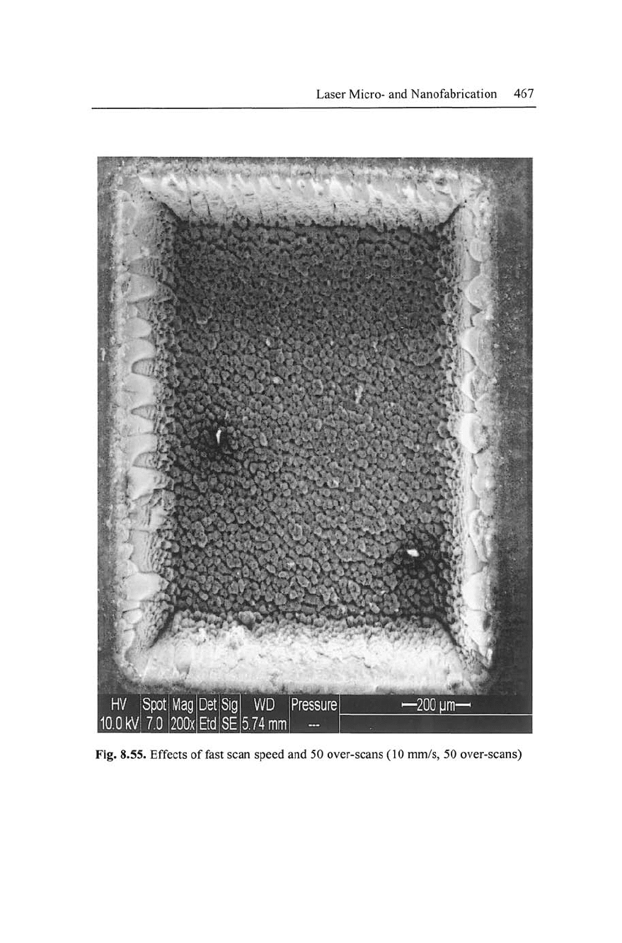
and many over-scans to achieve a reasonable depth. This was exam-
ined and is shown in Figure 8.54 where a scan speed of lOmm/s was
used to scan the surface 50 times. However, even with these pa-
rameters there is still significant texturing on the base (Figure 8.54).
Further experiments are required to conduct these experiments at
varying power levels, where it could be reasoned that at very low
power levels the formation of texture is reduced. The inherent prob-
lem with laser micromachining is the shape and nature of the Gaus-
sian beam profile. This problem is manifest in trenches where the
walls of
the
machined slot are not parallel.
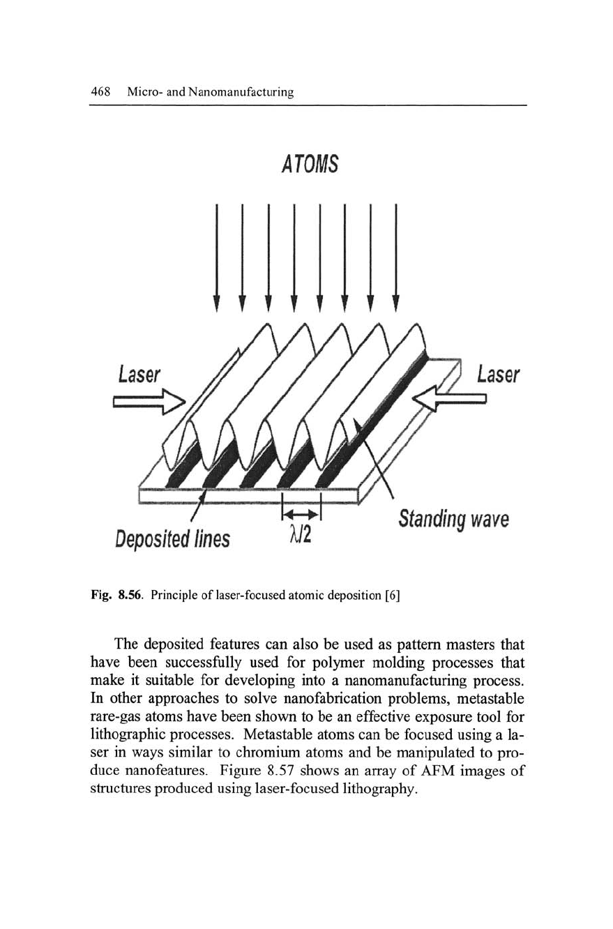
8.4 Laser Nanofabrication
Laser nanofabrication is being used to enhance processes such as
atomic force microscopy and molecular beam epitaxy by dispersing
accumulated atoms that forms "islands" of atoms from randomly de-
posited sources. Using the forces exerted by laser light that is tuned
to near atomic resolution, an array of atomic lenses is formed that
concentrates atoms in an array of lines with lengths of around 30
nm. This novel form of nanofabrication can create nanostructures
without the use of a resist or other pattern transfer technique. The
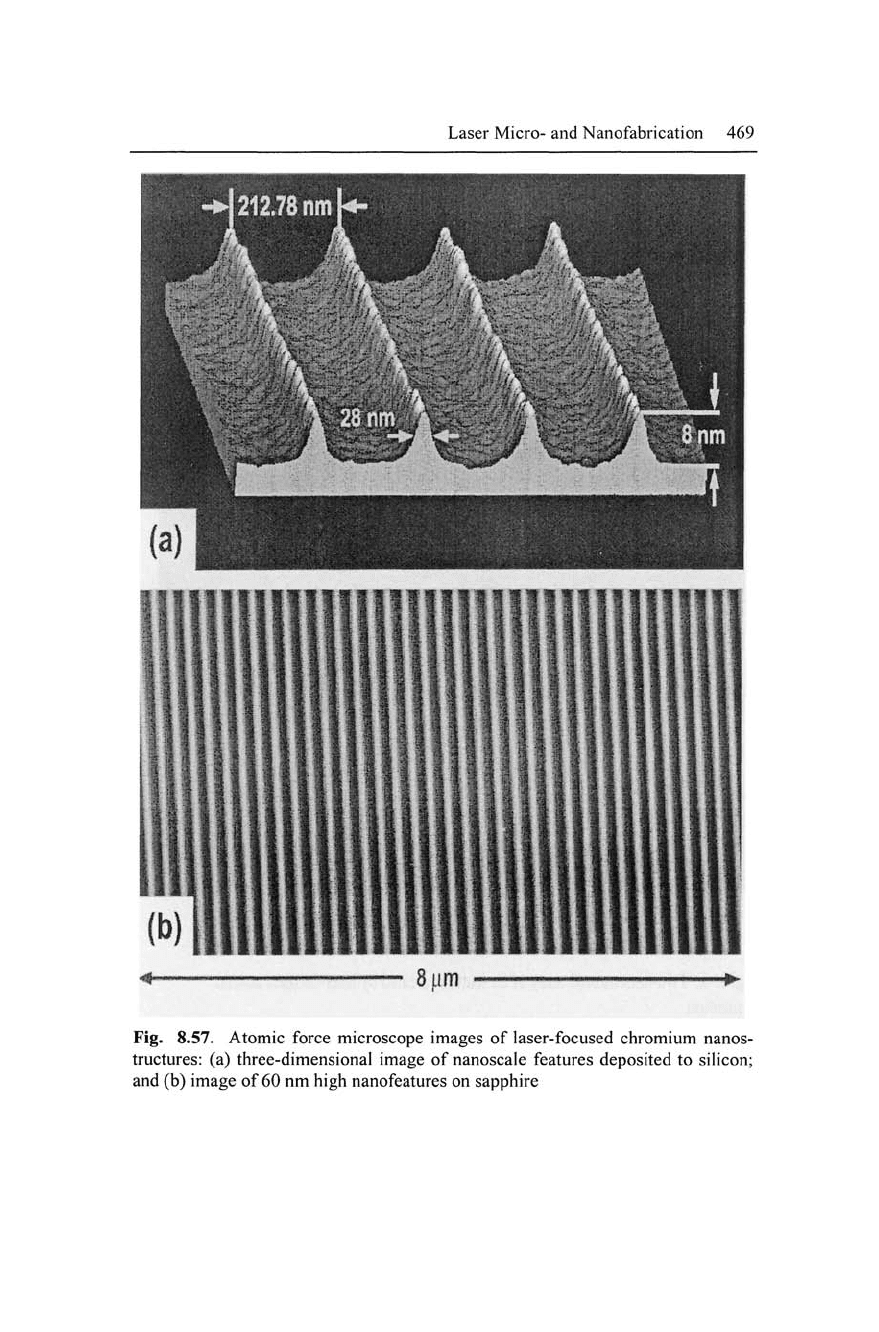
technique has been used to focus sodium, aluminium, and chromium
atoms by the force created by the nodes of the standing wave of light
that touches them. Laser-focused atomic deposition has been used
to create nanostructures of chromium atoms that are 60 nm in height
and 28 nm in width. Figure 8.56 shows the basic principle of laser
focused atomic deposition
[6-8].
The figure shows that atoms pass
through a near-resonant laser standing wave as they deposit to the
surface. An included dipole moment on the atom interacts with the
laser light to cause a force to act toward the nodes of the standing
wave. The resulting nanostructures are as small as 28 nm and are
spaced at half-a-wavelength.
Laser Micro- and Nanofabrication 465
;-:^t^"''
''^-^'tf-"
• ' •. .-^-^
Fig. 8.53. Trench structure variation at
1
mm/s and number of
over-scans:
(a) 1;
(b)2;(c)3;(ci)4;and(e)5
466 Micro- and Nanomanufacturing
Fig. 8.54. Trench structure variation at 21 over-scans and increasing scan speed
(mm/s):
(a) 1; (b) 2; (c) 3; (d) 4; and (e) 5
Laser Micro- and Nanofabrication 467
Fig. 8.55. Effects of fast scan speed and 50 over-scans (10 mm/s, 50 over-scans)
468 Micro- and Nanomanufacturing
ATOm
T
'
1 1 f
Laser
DBposited fines
Standing wave
Fig. 8.56. Principle of laser-focused atomic deposition [6]
The deposited features can also be used as pattern masters that
have been successfully used for polymer molding processes that
make it suitable for developing into a nanomanufacturing process.
In other approaches to solve nanofabrication problems, metastable
rare-gas atoms have been shown to be an effective exposure tool for
lithographic processes. Metastable atoms can be focused using a la-
ser in ways similar to chromium atoms and be manipulated to pro-
duce nanofeatures. Figure 8.57 shows an array of AFM images of
structures produced using laser-focused lithography.
Laser Micro- and Nanofabrication 469
8
Lim
Fig. 8.57. Atomic force microscope images of laser-focused chromium nanos-
tructures: (a) three-dimensional image of nanoscale features deposited to silicon;
and (b) image of 60 nm high nanofeatures on sapphire
470 Micro- and Nanomanufacturing
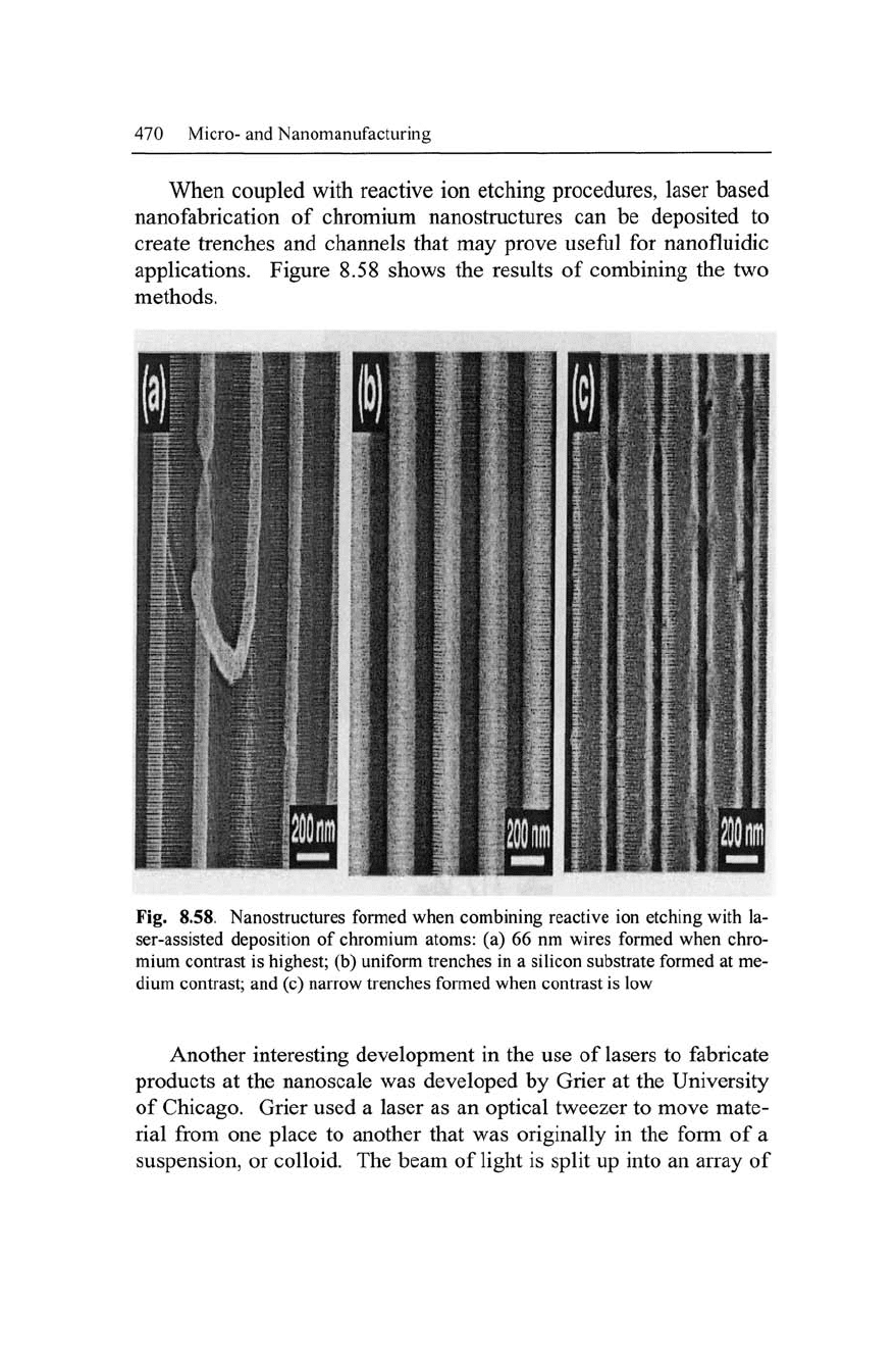
When coupled with reactive ion etching procedures, laser based
nanofabrication of chromium nanostructures can be deposited to
create trenches and channels that may prove useful for nanofluidic
applications. Figure 8.58 shows the results of combining the two
methods.
Fig. 8.58. Nanostructures formed when combining reactive ion etching with la-
ser-assisted deposition of chromium atoms: (a) 66 nm wires formed when chro-
mium contrast is highest; (b) uniform trenches in a sihcon substrate formed at me-
dium contrast; and (c) narrow trenches formed when contrast is low
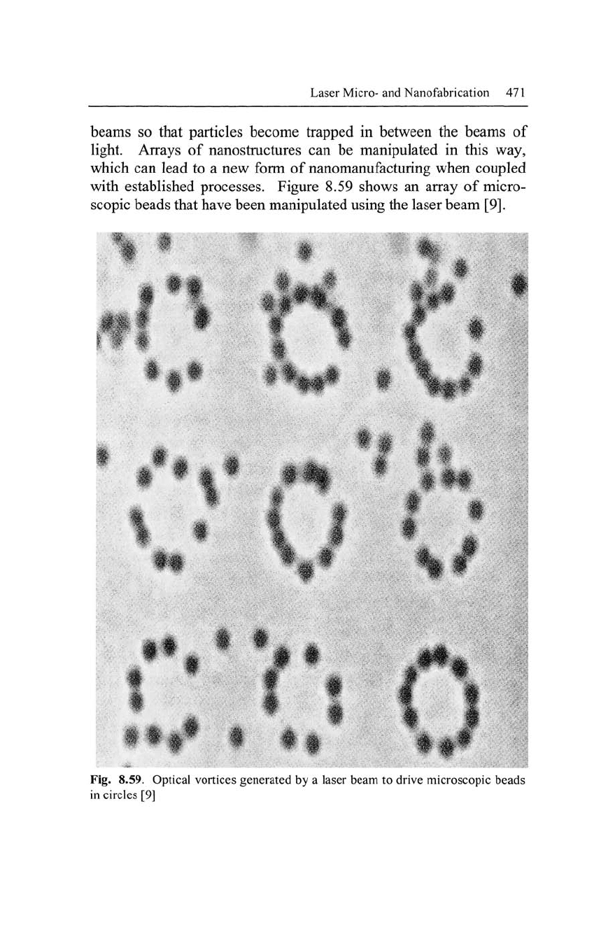
Another interesting development in the use of lasers to fabricate
products at the nanoscale was developed by Grier at the University
of Chicago. Grier used a laser as an optical tweezer to move mate-
rial from one place to another that was originally in the form of a
suspension, or colloid. The beam of light is split up into an array of
Laser Micro- and Nanofabrication 471
beams so that particles become trapped in between the beams of
Hght. Arrays of nanostmctures can be manipulated in this way,
which can lead to a new form of nanomanufacturing when coupled
with established processes. Figure 8.59 shows an array of micro-
scopic beads that have been manipulated using the laser beam [9].
*
f
i
i
Fig. 8.59. Optical vortices generated by a laser beam to drive microscopic beads
in circles [9]