Jackson M.J. Micro and Nanomanufacturing
Подождите немного. Документ загружается.

Manufacturing High Aspect Ratio Microstructures 131
3.10 Micromold Design
Most problems in micro-molding are not caused by the filling of the
mold, but by de-molding. During de-molding, microstructures may
be torn apart, deformed, or destroyed. De-molding affects the wear
of mold inserts and deUcate parts of
the
mold insert may even be de-
stroyed after a single molding process, the microstructure is not de-
signed properly or unsuitable molding parameters are chosen. It is
possible to de-mold microstructures with vertical sidewalls, but an
inclination angle of 2° reduces de-molding forces and is even more
important than the roughness of the sidewalls. An important factor
in de-molding is the shrinkage of the polymer, which occurs when
cooling down the polymer between the filling of the mold and de-
molding. Therefore, de-molding forces also are a function of the
orientation of microstructures relative to the direction of shrinkage
and the placement of critical microstructures relative to the center of
shrinkage. This is why the path of the polymer into the mold has to
be chosen with care for injection molding. Delicate microstructures,
such as pins with high aspect ratios, can be protected against shear-
ing forces resulting from shrinkage and mold filling by neighboring
auxiliary structures that are stable enough to withstand these forces.
If a mold insert is covered with areas microstructures of different
height, or varying density, then these areas should be arranged
symmetrically on the mold insert. In this way, tilting of the mold in-
sert during molding is avoided.
3.11 Micromolding Applications
Micromolding has been employed to fabricate a variety of polymer
components. Most applications are in the field of micro-optics and
micro-fluidics, but there are also some examples of micro-(and
nano) electrical and mechanical devices. The most widely sold mi-
cromolding product probably is the well known CD and DVD for
data storage, music, and videos. Another application is the holo-
gram that is attached to a credit card [14]. Other molded micro-
optical components include spectrometers [15], optical switches
[16,17],
optical fiber components [2], waveguides [18,19], anti-
132 Micro-and Nanomanufacturing
reflective surfaces [20], optical gratings [9, 21], and photonic struc-
tures [22]. There is a variety of molded microfluidic devices, such
as pumps [23-25], valves [26-28], nebulizers [29], ink jets [29], de-
gassers for HPLC systems [30], capillary analysis systems [29, 31-
34],
devices for investigations of living cells [29,35], pressure sen-
sors [36], and flow sensors [37]. Prospective applications of thermo-
plastic molding also lie in electronics. One of them is nano imprint-
ing [38-43] which may allow for the low-cost replication of
electronic circuits with critical dimensions as small as 10 nanome-
ters.
Other future electronic applications may be electronic and op-
tical circuit boards [19], acceleration sensors [44,45], and simple de-
vices,
such as electrical switches.
3.12 Limitations of IVIicromolding
What are limitations of micromolding of thermoplastic polymers?
Nanoimprinting processes show that structures of only a few tens of
nanometers in size are replicated very well. However, there is a
limitation regarding the achievable aspect ratio of columns, grooves,
and walls. This limit is a function of the geometry of the micro-
structure, its position on the sample, the polymer type, and the proc-
ess parameters. Finite element calculations could help solve mold-
ing problems of high-aspect-ratio microstructures, but FEM codes
are available for mold filling only and the limiting process step is
de-molding of the microstructures. Development of FEM calcula-
tions of de-molding operations has recently become available [46].
3.13 Fabrication of IVIoving IVIicrostructures
When silicon-based microstructures have been produced they
have to be separated from the base that holds them. This is usually a
glass substrate that can be sacrificially etched away using wet and
vapor etchants. Owing to surface tension effects, the glass material
usually sticks to the machined silicon. Techniques have been de-
signed to prevent sticking and are known as SCREAM, SIMPLE,
and BSM processes. These techniques are self-aligned and are suit-
Manufacturing High Aspect Ratio Microstructures 133
able for batch fabrication. The release of the structure takes place in
the gaseous phase, so that there is no problem associated with stic-
tion by fluids. This section of the chapter describes the study of
plasma release techniques for bulk and surface micromachining of
silicon based materials used for the fabrication of movable micro-
mechanical structures. Here, we discuss SCREAM and SIMPLE
processes.
3.13.1 Single Crystal Reactive Etching and Metallization
(SCREAM)
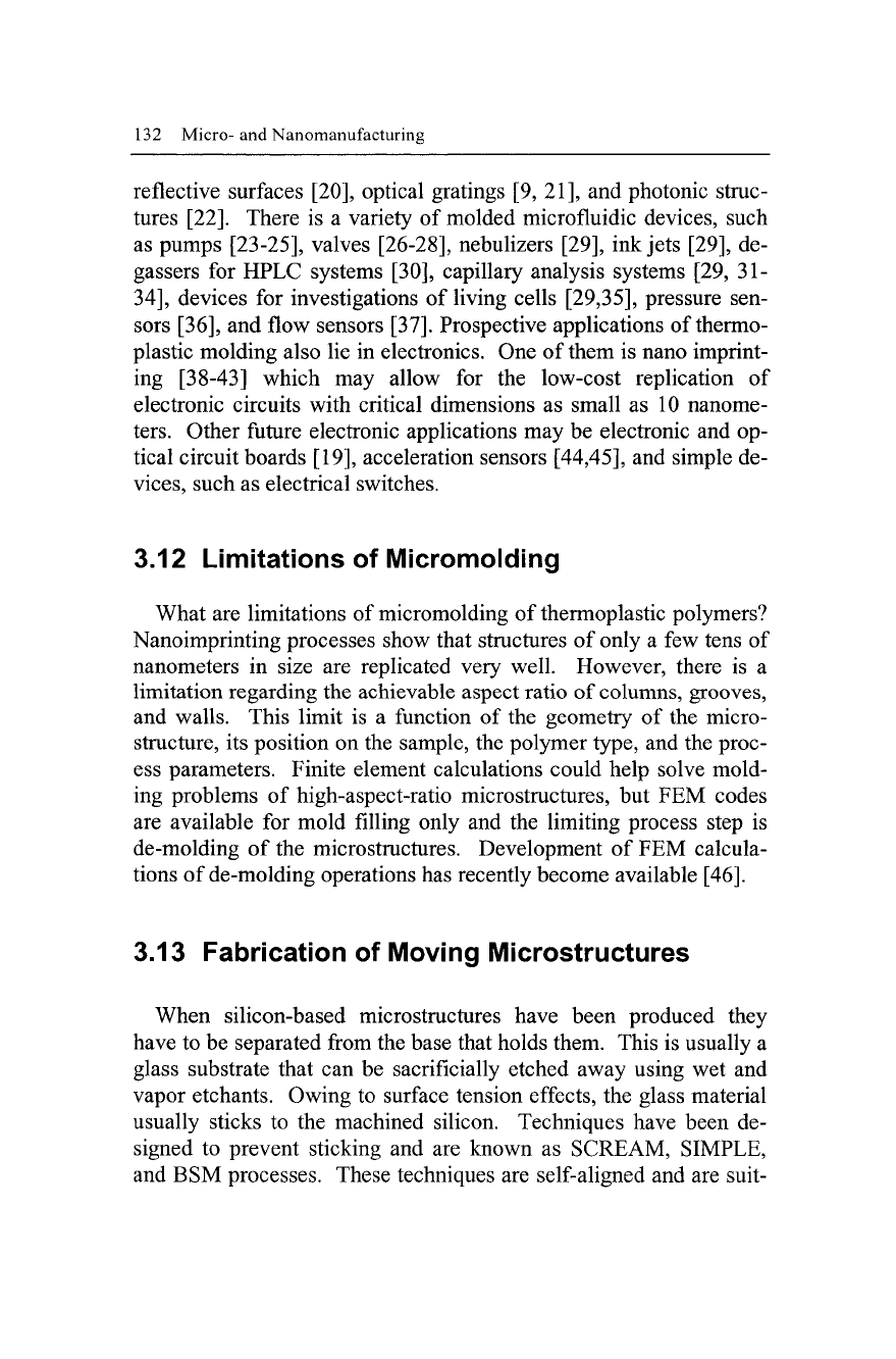
Single crystal reactive etching and metallization, or SCREAM, is
a process that consists of five basic steps (Fig. 3.19):
i^ IJJ Ul UJ ^ Ui
UMUMUi
MJ ^ IIJ IMJ
a. pip nm
amm
biSVRfffl c;BSI^SCS
c;Mi^ ^ tBim
Fig. 3.19. Dry plasma processes for manufacturing movable features: (a)
SCREAM; (b) SIMPLE; (c) BSM-SCS; (d) BSM-SOI; and (e) BSM-SISI [1]
134 Micro-and Nanomanufacturing
(1) Directional chlorine-based etching of silicon using the oxide
as a mask material;
(2) Trenches are passivated with the PECVD oxide;
(3) The oxide is then removed at the bottom of the trench using a
CHF3 plasma;
(4) An isotropic fluorine-based etch (SF6) will release the struc-
ture;
and
(5) For electrical contacting, a deposited metal layer is required.
There are some disadvantages with the process, such as:
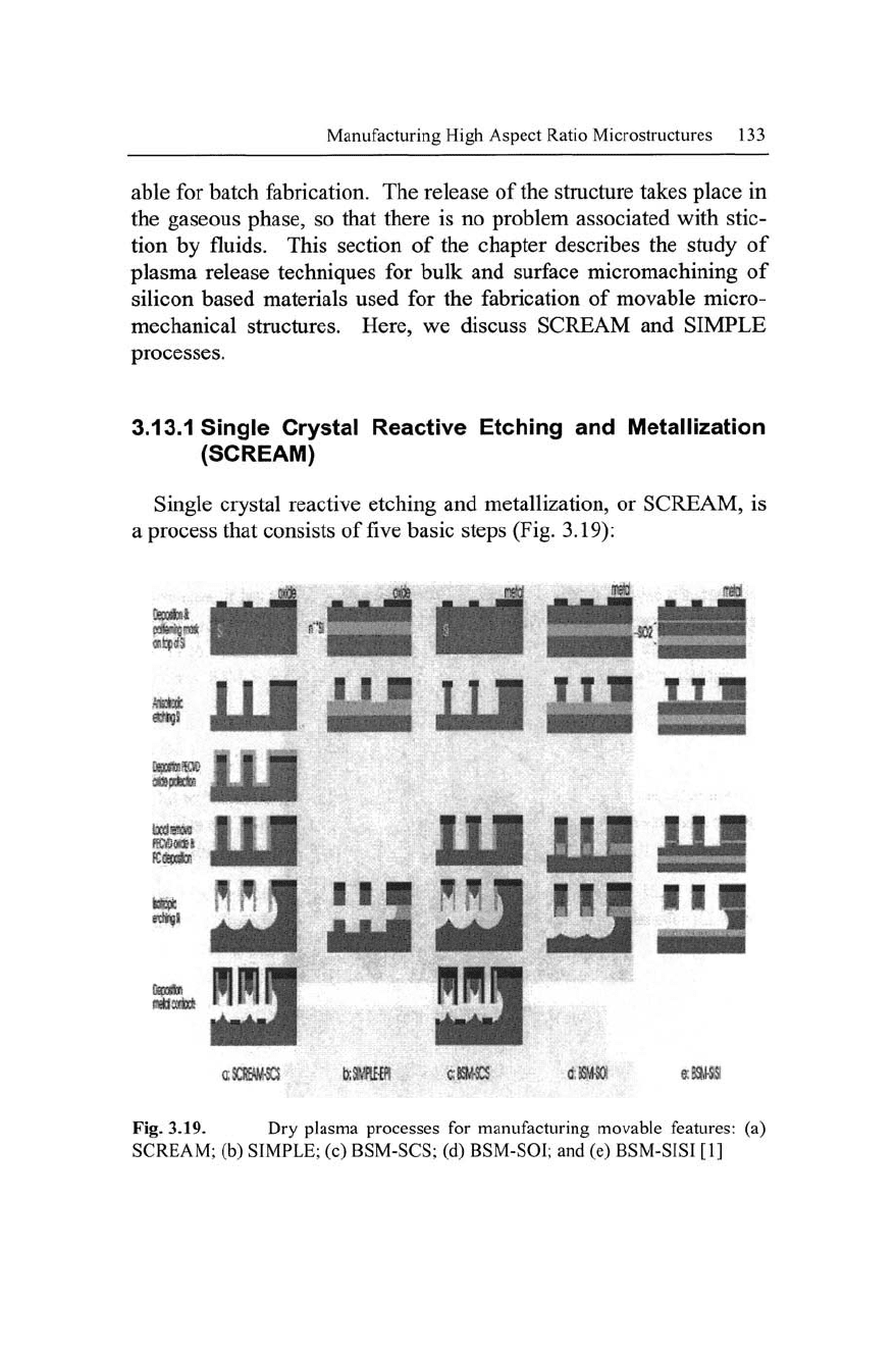
(1) The deposited PECVD layer should be tensile to avoid
buckling (Figure 3.20);
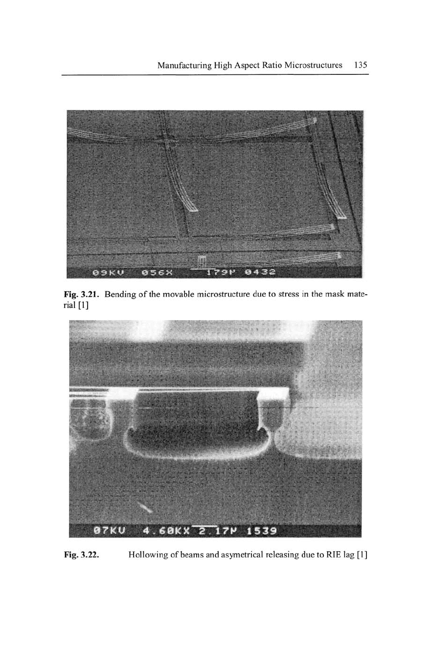
(2) The mask layer should be tensile to avoid bending after re-
lease (Figure 3.21);
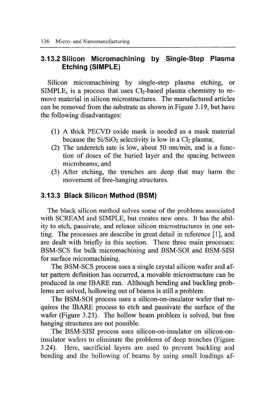
(3) The released structures are hollowed out during the isotropic
etch process (Figure 3.22); and
(4) RIE lag while etching Si directions may cause problems
during the isotropic etch because the etch depth may be
variable along the beam (Figure 3.22).
Fig. 3.20. Buckling of movable beam due to compressive stress [1]
Manufacturing High Aspect Ratio Microstructures 135
Fig. 3.21. Bending of the movable microstructure due to stress in the mask mate-
rial [1]
Fig. 3.22.
Hollowing of beams and asymetrical releasing due to RIE lag [1]
136 Micro-and Nanomanufacturing
3.13.2 Silicon IVIicromachining by Single-Step Plasma
Etching (SIMPLE)
Silicon micromachining by single-step plasma etching, or
SIMPLE, is a process that uses C^-based plasma chemistry to re-
move material in silicon microstructures. The manufactured articles
can be removed from the substrate as shown in Figure 3.19, but have
the following disadvantages:
(1) A thick PECVD oxide mask is needed as a mask material
because the Si/SiOz selectivity is low in a CI2 plasma;
(2) The underetch rate is low, about 50 nm/min, and is a func-
tion of doses of the buried layer and the spacing between
microbeams; and
(3) After etching, the trenches are deep that may harm the
movement of free-hanging structures.
3.13.3 Black Silicon Method (BSM)
The black silicon method solves some of the problems associated
with SCREAM and SIMPLE, but creates new ones. It has the abil-
ity to etch, passivate, and release silicon microstructures in one set-
ting. The processes are describe in great detail in reference [1], and
are dealt with briefly in this section. There three main processes:
BSM-SCS for bulk micromachining and BSM-SOI and BSM-SISI
for surface micromachining.
The BSM-SCS process uses a single crystal silicon wafer and af-
ter pattern definition has occurred, a movable microstructure can be
produced in one IBARE run. Although bending and buckling prob-
lems are solved, hollowing out of beams is still a problem.
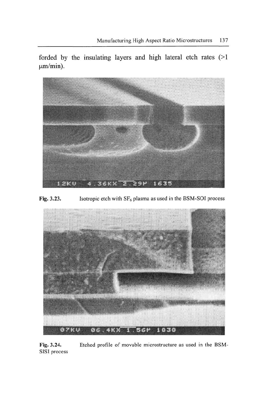
The BSM-SOI process uses a silicon-on-insulator wafer that re-
quires the IBARE process to etch and passivate the surface of the
wafer (Figure 3.23). The hollow beam problem is solved, but free
hanging structures are not possible.
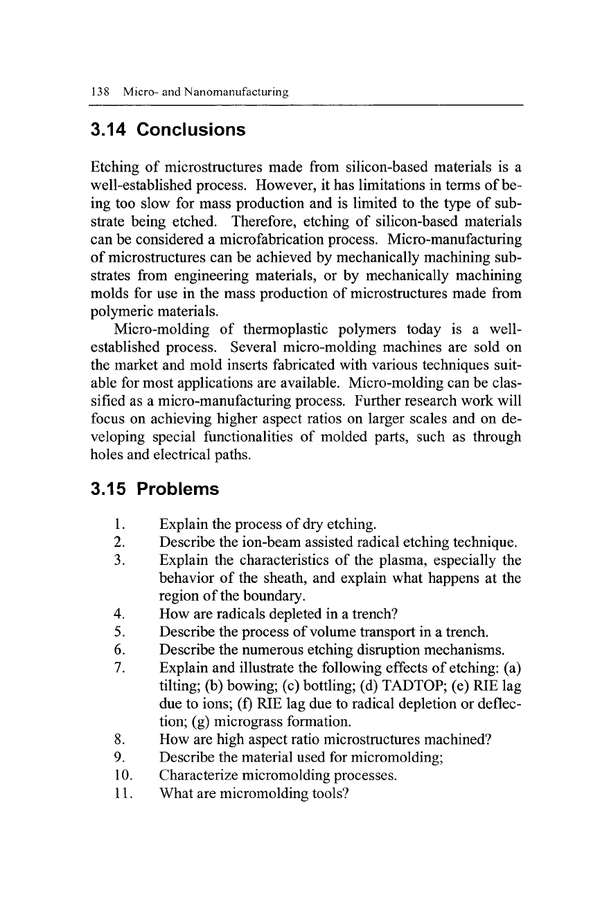
The BSM-SISI process uses silicon-on-insulator on silicon-on-
insulator wafers to eliminate the problems of deep trenches (Figure
3.24). Here, sacrificial layers are used to prevent buckling and
bending and the hollowing of beams by using small loadings af-
Manufacturing High Aspect Ratio Microstructures
137
forded
by the
insulating layers
and
high lateral etch rates
(>1
|Lim/min).
Fig. 3.23. Isotropic etch with SFg plasma
as
used
in
the BSM-SOI process
07KV 06.4KX^r756»* 1838
Fig. 3.24. Etched profile
of
movable microstructure
as
used
in the BSM-
SISI process
138 Micro-and Nanomanufacturing
3.14 Conclusions
Etching of microstructures made from silicon-based materials is a
well-established process. However, it has limitations in terms of
be-
ing too slow for mass production and is limited to the type of sub-
strate being etched. Therefore, etching of silicon-based materials
can be considered a microfabrication process. Micro-manufacturing
of microstructures can be achieved by mechanically machining sub-
strates from engineering materials, or by mechanically machining
molds for use in the mass production of microstructures made from
polymeric materials.
Micro-molding of thermoplastic polymers today is a well-
established process. Several micro-molding machines are sold on
the market and mold inserts fabricated with various techniques suit-
able for most applications are available. Micro-molding can be clas-
sified as a micro-manufacturing process. Further research work will
focus on achieving higher aspect ratios on larger scales and on de-
veloping special functionalities of molded parts, such as through
holes and electrical paths.
3.15 Problems
1.
Explain the process of dry etching.
2.
Describe the ion-beam assisted radical etching technique.
3.
Explain the characteristics of the plasma, especially the
behavior of the sheath, and explain what happens at the
region of the boundary.
4.
How are radicals depleted in a trench?
5.
Describe the process of volume transport in a trench.
6. Describe the numerous etching disruption mechanisms.
7.
Explain and illustrate the following effects of
etching:
(a)
tilting; (b) bowing; (c) bottling; (d) TADTOP; (e) RIE lag
due to ions; (f) RIE lag due to radical depletion or deflec-
tion; (g) micrograss formation.
8. How are high aspect ratio microstructures machined?
9. Describe the material used for micromolding;
10.
Characterize micromolding processes.
11.
What are micromolding tools?
Manufacturing High Aspect Ratio Microstructures 139
12.
How are micromolds designed?
References
1.
Elwenspoek J and Jansen H, Silicon Micromachining, Cambridge
University Press, 1998, Cambridge, U.K.
2.
Hanemann T, Heckele M and Plotter V, 2000, Current status of
micromolding technology, Polym. News, 25, 224-9.
3.
Wallrabe U, Dittrich H, Friedsam G, Hanemann Th, Mohr J,
Muller K, Plotter V, Ruther P, Schaller Th and ZiBler W, 2002, Micro-
molded easy-assembly multi fiber connector: RibCon, Microsyst. Tech-
nol.,
8, 83-7.
4.
Ehrfeld W, Bley P, Gotz F, Hagmann P, Maner A, Mohr J, Moser
H O, Miinchmeyer D, Schelb W, Schmidt D and Becker E W 1987 Fabri-
cation of microstructure using the LIGA process Proc. IEEE Micro-Robots
and Teleoperators Workshop (Hyannis, Cape Cod, MA, 9-11 Nov. 1987),
ed. K J Gabriel aad W S N Trimmer, IEEE Catalogue Number 87TH0204-
8.
5.
Hagmann P, Ehrfeld W and Vollmer H, 1987, Fabrication of mi-
crostructures with extreme structural heights by reaction injection molding,
First Meeting of the European Polymer Federation European Symp. On
Polymeric Materials, (Lyon, France, 14-18 Sept.), paper EPD05.
6. Heckele M, Bacher W and Mtiller K D, 1998, Hot embossing-the
molding technique for plastic microstructures, Microsyst. Technol., 4, 122-
4.
7.
Rogge T, Rummler Z and Schomburg W K, 2002, Piezo-driven
polymer microvalve manufactured by the AMANDA process, Proc. of Eu-
rosensors XVI, (Prague, 15-18 Sept. 2002), pp 214-7.
8. Niggemann M, Blaesi B, Boemer V, Gombert A, Klicker M, Kue-
bler V, Lalanne P and Wittwer V, 2001, Periodic microstructures for large
area applications generated by holography,
Conf.
Physics. Theory, and
Applications of Periodic Structures in Optics, (San Diego, CA, 1-2 Aug.
2001),
Proc. SPIE 4438,108-15.
9. Jian L, Desta Y M and Goettert J, 2001, Multilevel microstructures
and mold inserts fabricated with planar and oblique x-ray lithography of
SU-8 negative photoresist, Conf Micromachining and Microfabrication
Process Technology VII, (San Francisco, CA, 22-24 Oct. 2001), Proc.
SPIE 4557, 69-76.
10.
O'Donnell T, McCloskey P, Brunet M, Winfield R, Mathuna S C
O, Stephen A and Metev S, 2000, High aspect ratio RF coils fabricated us-
140 Micro-
and
Nanomanufacturing
ing laser processing
and
micro-molding techniques, Proc. European
Mi-
croelectronics Packaging
and
Interconnection Symposium, (Prague, Czech
Republic,
18-20
June 2000),
pp
169-74, ISBN: 80-238-5509-3.
11.
Mohr
J, 1998,
LIGA-A technology
for
fabricating microstructures
and microsystems. Sensors Mater.,
10,
363-7.
12.
Chung
S,
Hein
H,
Mohr
J,
Pantenburg
J-J and
Wallrabe
U,
2000,
LIGA technology today
and its
industrial applications, Proc. SPIEs
Int.
Conf
on
Microrobotics
and
Microassembly
II,
(Boston,
5-6 Nov.
2000),
Proc.
SPIE 4184,44-55.
13.
Martynova
L,
Locascio
L E,
Gaitan
M,
Kramer
G W,
Christensen
R
G and
MacCrehan
W
A, 1997, Fabrication of plastic microfluid channels
by imprinting methods,
Ann.
Chem., 69,4783-9.
14.
Haines
K,
1996, Development
of
embossed holograms, Proc. SPIE
2652,
45-52.
15.
Heckele
M, 1997,
Aufbau
und
Betrieb einer Kleinserienfertigung
von LIGA-Spektrometem, Swiss Plastics,
19, 5-9.
16.
Shan
X C and
Maeda
R,
2002, Development
of a
low-cost
8x8
optical switch using micro-hot embossing 2002 lEEE/LEOS
Int.
Conf
Op-
tical MEMS (Lugano, Switzerland, 20-23
Aug.
2002, IEEE (2002)),
pp
21-
2 (Catalogue
no
02EX610), ISBN: 0-7803-7595-5.
17.
Hashiura
Y,
Ikehara
T,
Kitajima
A,
Goto
H and
Maeda
R, 2001,
Optical switch array based
on
microforming process,
Conf.
Device
and
Process Technologies
for
MEMS
and
Microelectronics (Adelaide,
SA,
Austraha,
17-19
Dec. 2001), Proc. SPIE, 4592,
414-21.
18.
Ulrich
R,
Weber
H P,
Chandross
E A,
Tomlinson
W J and
Franke
E
A,
1972, Embossed optical waveguides, Appl. Phys. Lett.,
20,
213-5.
19.
Krabe
D and
Scheel
W, 1999,
Optical interconnects
by hot em-
bossing
for
module
and PCB
technology-the
EOB
approach, Proc. 49th
Electronic Components
and
Technology Conference
(San
Diego,
CA,
USA,
1-4
June
1999)
(Catalogue
no
99CH36299), ISBN: 0-7803-5231-9,
pp 1164-6.
20.
David
C,
Haberling
P,
Schnieper
M,
Sochtig
J and
Zschokke
C,
2002,
Nano-structured anti-reflective surfaces replicated
by hot
embossing,
Microelectron.
Eng.,
61-62,435-40.
21.
Knop
K 1976,
Color pictures using
the
zero diffraction order
of
phase grating structures.
Opt.
Commun., 18, 298-303.
22.
Grigaliunas
V,
Kopustinskas
V,
Meskinis
S,
Margelevicius
M,
Mikulskas
I and
Tomasiunas
R,
2001, Replication technology
for
photonic
band
gap
applications, Conf Optoelectronics
I,
Materials
and
Technolo-
gies
for
Optoelectronics Devices, Symposium
G of the
2000 E-MRS-
lUMRS-ICEM Spring
Conf.,
(Strasbourg, France,
20
May-2 June 2000),
Opt. Mater.,
17, 15-8.