Hawkes P.W., Spence J.C.H. (Eds.) Science of Microscopy. V.1 and 2
Подождите немного. Документ загружается.

Chapter 4 Analytical Electron Microscopy 355
broadening to r
c
(β) ≈ β∆f. Once again, two cases can be distinguished:
∆f = C
c
(E/E
0
) if the image is focused at the primary energy E
0
and ∆f =
C
c
(∆E/4E
0
) if the electrons are focused at an energy loss of interest and
an energy selecting slit ∆E wide is used (Egerton, 1996).
The broadening due to aberrations is a signifi cant contribution that
cannot be reduced in current instrumentation, although work is in
progress to develop chromatic aberration correctors that would signifi -
cantly impact the ultimate resolution in energy-fi ltered imaging. Thus,
at the present time, the ultimate resolution is achieved by limiting the
illuminated area with the electron beam. Current commercial Schottky-
type FEG instruments make it possible to achieve a probe size of about
0.2 nm with typically 10 pA of current (more with a cold fi eld emission
source). Spherical aberration correctors can be used to improve the
probe-forming capability. These instruments have already been devel-
oped and implemented on different platforms by major manufacturers
on both dedicated scanning transmission microscopes and STEM-TEM
instruments yielding sub-Ångstrom probes with 10–20 pA current
or about a few hundred picoamperes for 0.2-nm-diameter probes
[Dellby et al., 2001; Krivanek et al., 2003; Batson et al., 2002; Krivanek
et al., 2003; and Chapter 2 (this volume)]. With such small probes,
however, it becomes increasingly important to be aware of the detailed
electron propagation within the sample as discussed in Section 3.2.
Since the electron propagation process in the sample is the same
irrespective of the microanalysis technique probing various signals,
elastic scattering does affect the broadening of the electron beam not
only in EDXS but also in EELS measurements. The impact of this
broadening on the degradation of the spatial resolution, however, can
be somewhat controlled with the use of a collection aperture that limits
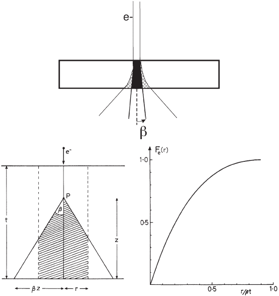
the scattering angles entering the spectrometer. As shown in Figure
4–72a, electrons scattered at high angles (thus away from the forward
direction and the incident probe distribution) can be eliminated with
the use of an angle-limiting collection aperture (either the objective
aperture if the spectra are acquired in image mode or the spectrometer
aperture if the spectra are acquired in diffraction and STEM mode).
Assuming that the elastic scattering distribution is large compared to
the collection angle and that there is no strong Bragg scattering (essen-
tially an amorphous sample) the fraction of electrons contained within
a radius r for a given sample thickness t and collection aperture β can
be estimated geometrically (Figure 4–72b and c). Based on Figure 4–
72b we can estimate this geometric broadening contribution for a par-
allel incident electron beam. For a sample thickness of 100 nm and a
collection angle of 10 mrad, the fraction of electrons contained within
0.5 nm would be 85% and nearly 100% for 1 nm. These contributions
can be small compared to the intrinsic broadening due to the conver-
gence of the electron beam required for STEM imaging and optimal
probe size (in the range from a few millirad to a few tens of millirad
in the case of aberration-corrected STEM instruments (see Section 2.1).
The latter geometric broadening contribution for a 100-nm-thick sample
assuming optimal probe size with 30 mrad convergence in an aberra-
tion corrected STEM would be 3 nm! Although these numbers repre-
356 G. Botton
sent an extreme effect due to the sample thickness, typical samples
used to demonstrate the ultimate resolution tend to be in the order of
5–10 nm thick as required to limit the propagation of the electron beam
within a single atomic column (Section 3.2). In these cases, the geomet-
ric broadening would be of the order of 0.1–0.3 nm.
When the electron beam size is in the order of a fraction of a nano-
meter, a signifi cant contribution affecting the spatial resolution is the
delocalization of inelastic scattering, i.e., the excitation and energy loss
can occur even for electrons traveling at a fi nite distance b from the
target atoms and not only when the incident electron is “directly on
the atom” in the classical particle point of view. This factor ultimately
limits the spatial resolution in EELS analysis with aberration-corrected
electron microscopes capable of achieving sub-Ångstrom beam sizes.
As expected from the wave-mechanical perspective, the origins of
the delocalization effect are quantum mechanical in nature and relate
a)
b) c)
Figure 4–72. Geometric contribution to the broadening of the electron beam.
(a) The effective broadening can be reduced by using an angle-limiting aper-
ture even if the real broadening still occurs in the sample as larger scattering
angles (causing the broadening) are cut off by the aperture. (b) Diagram defi n-
ing the broadening terms necessary to calculate the fraction of electrons scat-
tered outside a radius r for a given combination of thickness and collection
aperture. (c) Geometric evaluation of the fraction of electrons contained within
a radius r. (From Egerton © 1996, with permission from Springer Science+Business
Media.)

Chapter 4 Analytical Electron Microscopy 357
to the uncertainty relation, but a simple classical treatment makes it
possible to identify the signifi cant elements related to spatial resolu-
tion. Based on classical scattering, the impact parameter b is related to
the scattering angle of electrons (Figure 4–40): large scattering angles
are indicative of a smaller impact parameter and thus interactions
closer to the atom. Hence, measurement of energy losses carried out
on electrons scattered at a large scattering angle would imply higher
apparent resolution. The simplest treatment of the spatial resolution
involving the uncertainty principle (e.g., Brown, 1999) invokes the time
of interaction (∆τ) of an electron traveling at a speed v and at a distance
b from the atom. The interaction time is ∆τ = b/v. Applying the uncer-
tainty relation ∆E∆τ ≤ h yields b
max
= hv/∆E with b considered the ulti-
mate spatial resolution and ∆E the energy loss. For energy losses of
about 20 eV (at 100 keV) the delocalization is of the order of 2 nm while
for energy losses of 200 eV it would be 0.2 nm. A more detailed analysis
(Pennycook, 1982; Pennycook et al., 1996) based on the same principles
yields a delocalization with the form
b
v
E
=+
()
+
−
β
βθ
β
θ
∆
22
2
2
12
1
E
E
ln
(64)
where β is the limiting collection angle (the maximum scattering angle
entering the spectrometer) and θ
E
is the characteristic scattering angle
at the energy loss ∆E (θ
E
= ∆E/2E
0
).
The detailed quantum mechanical treatments by Muller and Silcox
(1995) and Kohl and Rose (1985) as well as the work of Pennycook (1982)
led to results (in terms of trends and order of magnitude) similar to the
simpler analysis presented by Egerton (1996, 1999), who considered a
spatial resolution related to the diffraction limit imposed by the width
of the energy-dependent scattering distribution and the collection aper-
ture. This approach can be deduced as follows. For high energy losses,
the angular distribution can be broader than the collection aperture
and thus the diffraction limit imposes a resolution determined by the
collection aperture β similar to the Rayleigh criterion, i.e., 0.6λ/β.
When the angular scattering distribution is not limited by the col-
lection aperture (typically for low energy losses), the scattering distri-
bution is limited by a cut-off angle θ
c
= (2θ
E
)
1/2
related to the Bethe-ridge
maximum scattering angle (Sections 3.3 and 3.4.1). In this case, the
median scattering θ
˜
angle containing 50% of the electrons is θ
˜
≈ (θ
E
θ
c
)
1/2
and thus θ
˜
≈ 1.2(θ
E
)
3/4
. By considering that the limiting aperture con-
taining 50% of the electrons is effectively given by θ
˜
, this diffraction
limit contribution will be 0.6λ/θ
˜
, i.e., 0.5λ/(θ
E
)
3/4
. Combining the two
limiting terms in quadrature, the delocalization contribution to the
resolution, related to inelastic scattering of 50% of the intensity, is
d
50
34
2
2
05 06
≈
(
)
[]
+
(
)
..λθ λβ
E
(65)
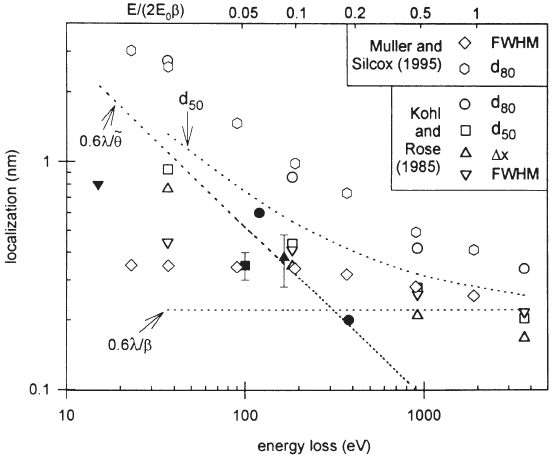
Experimental measurements roughly agree with these estimates and
more detailed quantum mechanical treatments (Kohl and Rose, 1985;
Muller and Silcox, 1995) (Figure 4–73). More recent work deals with the
impact of aberration correction and ultimate spatial resolution by com-
bining the effects of inelastic scattering and sub-Ångstrom beam prop-
358 G. Botton
agation in the sample (Oxley et al., 2005; Cosgriff et al., 2005; Dwyer,
2005). This delocalization contribution enters the defi nition of resolu-
tion for energy-fi ltered elemental mapping (Section 6.2.3). It is impor-
tant to note that elastic scattering can affect the apparent resolution
shown in inelastic images due to the modulation of the signal entering
the spectrometer. If strong elastic contrast is present (for example,
lattice fringes, larger atomic number elements, or diffraction contrast),
inelastic images might show features with apparent resolution that is
not simply related to the inelastic scattering distribution but rather to
the much more localized elastic scattering (Spence and Lynch, 1982).
Lattice images obtained with inelastically scattered electrons can be
obtained, therefore, at energy losses where the localization contribu-
tion is, in principle, larger than the interatomic spacing due to these
effects. As discussed in Section 6.2, approaches have been devised to
circumvent these effects by selecting the collection aperture so that the
phase contrast, giving rise to lattice images, disappears and by normal-
izing the inelastic images with the background prior to the edge thresh-
old (Freitag and Mader, 1999; Hofer et al., 2000).
6 Elemental Mapping
6.1 Elemental Mapping EDXS
With the control of scanning coils of the electron microscope (Section
2.2) and by recording X-ray counts within a particular energy window
Figure 4–73. Localization of inelastic scattering as a function of energy loss
for a collection angle β of 10 mrad. Curves are based on a Rayleigh approach
to the evaluation of the localization. Various experimental measurements
based on the literature are presented (fi lled symbols). (From Egerton, 1996.)
Chapter 4 Analytical Electron Microscopy 359
of interest under a characteristic peak or even the full spectrum at each
pixel of a rastered area, it is possible to combine the intensity recorded
for each element into a map to display the distribution of elements in
the sample with a resolution appropriate to the experimental condi-
tions and sample thickness. Due to the long recording time at each
pixel necessary to obtain a statistically signifi cant number of counts at
each pixel and still maintain a small probe size compatible with the
spatial resolution of the technique, the acquisition of elemental maps
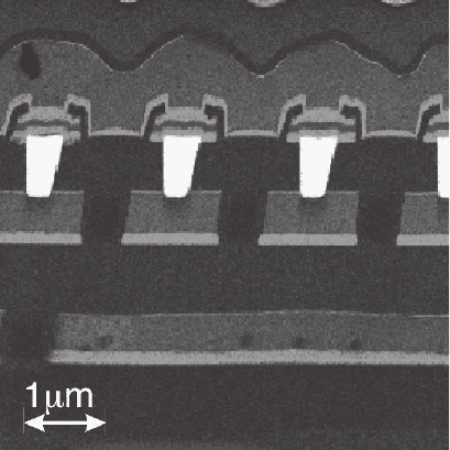
with EDXS can take several minutes to a few hours. Examples of
such maps in the case of semiconductor materials are shown in Figures
4–69 and 4–74. Although simple unprocessed elemental maps provide
a wealth of information on the distribution of elements, it is also pos-
sible to extract quantitative information on the concentration of ele-
ments based on the use of ratios of images and the use of k-factor
analysis. Relative concentration maps for elements A and B can thus
be obtained by processing the entire image rather than just integrated
intensities under an energy window. The quantitative concentration
map can be obtained as I
C
A
/
C
B
(x,y) = k
AB
[I
A
(x,y)/I
B
(x,y)] where k
AB
is the
Cliff–Lorimer factor discussed in Section 4.1.1 and I
A,B
(x,y) are the ele-
mental maps for elements A and B, respectively. Each elemental map
has a background image (obtained by recording the intensity within
a window where no characteristic peak is visible) subtracted prior to
the quantifi cation. The division is carried out pixel by pixel with the
constant k
AB
factor.
If absorption is not signifi cant, relative concentration maps are insen-
sitive to changes in thickness. Therefore, although raw elemental maps
show changes in intensity related to variations in the projected density
Figure 4–74. Color-coded elemental map of a device showing the distribution
of elements in the rastered area: red, Al-rich area; blue, Si-rich area; green, Ti-
rich area. White, W. Interdiffusion of Si into the Al is noted through the bottom
barrier layer containing Ti. (See color plate.)
360 G. Botton
of atoms with changes in thickness, the ratio map does not (Figure 4–
75). When absorption is signifi cant, this simple approach fails and
absorption correction is required. For this correction, the sample thick-
ness must be determined. To deal with strong absorption cases without
calculation of the absorption correction factor (Section 4.1.2), quantifi -
cation of maps through the ζ-factor approach have been proposed
(Williams et al., 2003; Watanabe et al., 1996; Watanabe and Williams,
1999).
The technique makes it possible to circumvent the problem of having
to determine the sample thickness independently (with intrinsic large
errors) by calculating the absorption correction composition and the
sample thickness simultaneously. The ζ-factor relates the intensity and
composition of a standard sample to the mass thickness for both ele-
ments A and B as
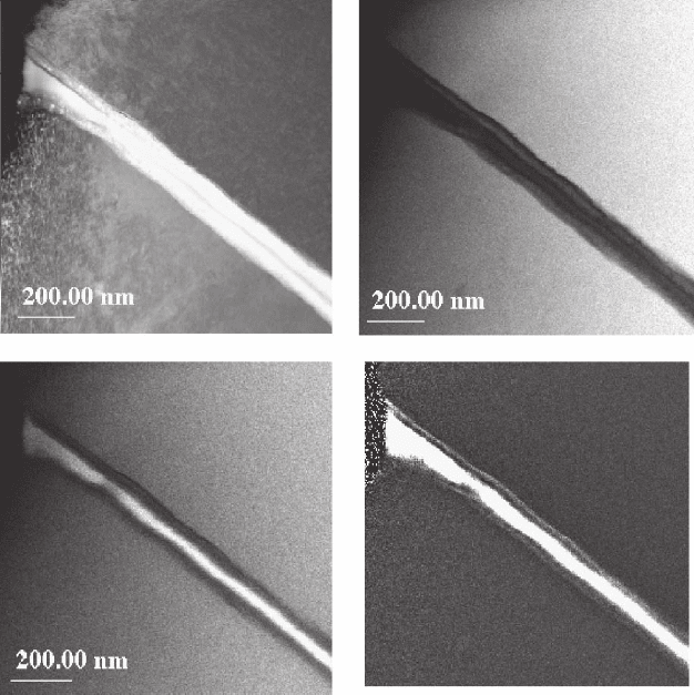
a) Dark field image STEM b) Ni map
c) Cr ma
p
d) Cr/Ni ma
p
Figure 4–75. Elemental maps of Ni-based alloy with intergranular product.
(a) STEM image; (b) Ni map showing the variation of intensity due to thickness
variations (from the top left corner to the bottom right corner); (c) Cr elemental
map with similar variations in intensity due to thickness; (d) elemental ratio
map for Ni/Cr demonstrating the correction of the thickness variations in the
maps. The intergranular product contains a Cr-rich carbide phase surrounded
by oxidation product. (See color plate.)
Chapter 4 Analytical Electron Microscopy 361
ρζ ρζt
I
C
t
I
C
==
A
A
A
B
B
B
and (66)
where I
A,B
are the intensities recorded for elements A and B and C
A,B
are the concentrations of the same elements. If the ζ-factors are
determined through measurements of standards of known composi-
tion and thickness via Eq. (66) the concentrations are deduced as
(Williams et al., 2003)
C
I
II
C
I
II
tI I
A
AA
AA BB
B
BB
AA BB
AA BB
,,=
+
=
+
=+
ζ
ζζ
ζ
ζζ
ρζζ
(67)
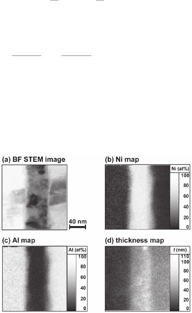
Quantitative concentration and thickness maps accounting for this
effect have been demonstrated (Figure 4–76).
Advanced analysis techniques based on the full processing of the
spectrum and multivariate analysis make it possible to extract the
occurrence of the various phases without prior knowledge of the indi-
vidual component phases within the samples. Examples of multivari-
ate analysis at high spatial resolution have been demonstrated in AEM
(Kotula et al., 2003) following initial developments in SEM (Kotula
et al., 2001) and earlier work of line profi les by Titchmarsh and Dumbill
(1996) and Chevalier and Botton (1999). These techniques are particu-
Figure 4–76. Quantitative elemental maps of an NiAl multilayer obtained with the ζ-factor approach.
The gray scale represents the quantitative information on sample composition including correction
for absorption. (Reprinted from Williams et al. © 2003, with permission from Elsevier.)
362 G. Botton
larly useful for the analysis of segregation at grain boundaries and
interfacial phases.
6.2 EELS Mapping
6.2.1 Energy-Filtered TEM Mapping
With both postcolumn and in-column energy fi lters described in
Section 2.4.1, it is possible to retrieve images at specifi c energy losses
by taking advantage of an energy selected slit. These images can show
the distribution of elements following the extraction of the background
from the images. Recent reviews of the technique and the applications
have been given in Hofer and Warbichler (2004), Verbeeck et al. (2004),
and Hofer et al. (2000), and we will summarize the approaches here.
In the basic approach of energy-fi ltered elemental mapping, this extrac-
tion of element-specifi c images can be achieved through two different
methods: the three-window technique and the jump-ratio technique.
In both cases, energy-selected images at selected energy losses
must be taken before the ionization edge and at the edge of interest
(Figure 4–77).
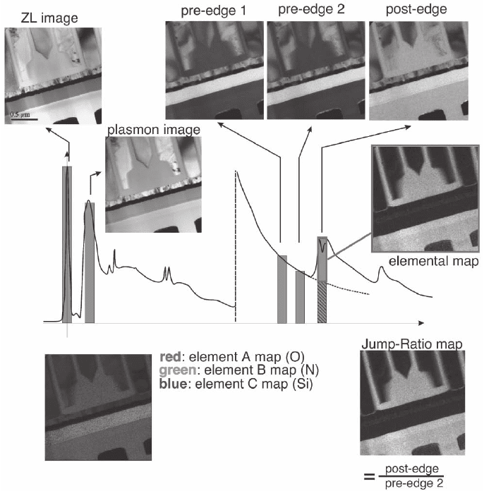
In the three-window method, two energy-fi ltered images (called
preedge images) acquired prior to the edge onset are used to extrapo-
late the noncharacteristic background under the edge where the third
energy-fi ltered image (called postedge image) has been acquired. The
same power-law extrapolation model used for quantitative analysis is
used [namely, I
b
(E) = AE
−r
] using the two preedge windows. The ele-
mental map is then obtained by subtraction of the background image
from the postedge image. Because there are only two images for this
extrapolation, the resulting error in the intensity of the postedge back-
ground image, and thus the subtraction, can be large. If the intensity
in the recorded images is low and the background varies steeply at the
energy loss of interest, spurious images with negative extracted inten-
sity can often be obtained because the variance in the extrapolation
can be larger than the intensity of the ionization edge. Since the signal
in the ionization edge is related to the ionization cross section and the
number of atoms (Section 4.2.1) images represent the quantitative dis-
tribution of elements within the fi eld of view.
The second approach to ext ract the dist ribut ion of elements is th rough
jump ratio images. In this case, the postedge image is divided by one of
the preedge images (generally obtained just before the edge threshold).
Although these images are not directly quantifi able, they have the
advantage that the noise is lower (no extrapolation is involved), the
elastic contrast (due to diffraction, high atomic number, and phase con-
trast) is canceled as it affects both the preedge and postedge images in
a similar way, and fi nally there is less drift involved as only two images
are used (and thus a shorter acquisition time) (Verbeeck et al., 2004).
This latter point signifi cantly affects the spatial resolution of images as
discussed below. Both methods can be applied with energy fi lters (irre-
spective of whether they are in-column or postcolumn) and also in
STEM instruments equipped with serial spectrometers allowing the
acquisition of energy-fi ltered images through an energy-selecting slit.
Chapter 4 Analytical Electron Microscopy 363
Early serial spectrometers on dedicated VG-STEM and the fi rst serial
spectrometers from Gatan both equipped with scintillators and photo-
multipliers served this purpose. Parallel spectrometers and imaging
fi lters equipped with single-channel photomultiplier detectors
(Krivanek et al., 1994) or a fast array of photomultipliers (developed by
the Ottensmeyer group in Toronto) (Ottensmeyer, 2004) were also
developed in prototype systems but were superseded by the develop-
ment of much faster detectors allowing the acquisition of full spectra at
each pixel of the rastered area as discussed in Section 6.2.2.
In addition to these basic energy-fi ltered TEM (EFTEM) acquisition
techniques, there have been variants of the three-window and jump-
ratio methods for EELS imaging based on the development of more
advanced acquisition software controlling the spectrometer, the micro-
scope, and increased storage capabilities in desktop computers. One
variant is the EFTEM-spectrum imaging method initially proposed by
Figure 4–77. Various approaches to EFTEM imaging. Zero-loss (ZL) fi ltered imaging (selecting only
electrons that have lost no signifi cant amounts of energy), plasmon imaging (selecting only electrons
that have lost energy in the 10–30 eV range), and core loss imaging with the three-windows technique
(extrapolation of the background under the edge) and the jump-ratio technique. (See color plate.)
364 G. Botton
Lavergne et al. (1992) and fully developed as very powerful tools for
mapping and quantitative analysis by Mayer et al. (1997) and Thomas
and Midgley (2001a,b). This technique is now implemented in com-
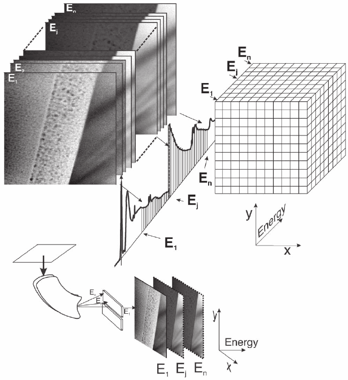
mercial packages from energy fi lter vendors. The method is based on
the acquisition of an information data cube consisting of a large number
of energy-fi ltered images with narrow energy windows (from 1–2 to
5–10 eV) and small step intervals making it possible to cover large
energy ranges around the edges [in some cases even from 0 eV to the
characteristic core losses (Thomas and Midgley, 2001b)] so that the full
information from the spatial distribution and energy loss can be
retrieved with high spatial sampling (Figure 4–78). If the spatial drift
of the sample is well corrected in the image stack using automated
Figure 4–78. Schematic description the energy-fi ltered TEM spectrum imaging technique (EFTEM-
SI). Each image obtained at a given energy loss is part of a three-dimensional data cube containing
information on the distribution of elements. The technique provides detailed sampling of the spatial
information with little sampling of the energy loss distribution (energy window widths can vary from
less than 1 to 10 eV).
