Hawkes P.W., Spence J.C.H. (Eds.) Science of Microscopy. V.1 and 2
Подождите немного. Документ загружается.

Chapter 3 Scanning Electron Microscopy 225
operated over a wide retarding range of potentials (0.1–10 kV). The
instrument has an optimized design (mircoeinzel lens followed by a
retarding region) to minimize the primary beam diameter and to maxi-
mize secondary electron collection (approximately 50% of SE are
collected).
3.2.2 Detectors and Detection Strategies
As mentioned previously, modern commercial FESEMs can operate
usually from 30 keV down to 1 keV or even 0.5 keV; the commonly used
detectors and detection strategies of these instruments were discussed
in Sections 2.1.3 and 3.1.3. It is clear from Figure 3–12 that the lower
the energy E
0
of the beam electrons the lower the energy difference
between the secondary and backscattered electrons. The lower the dif-
ference of the different signal electrons the more diffi cult is their sepa-
ration. At very low electron landing energies SE and BSE are almost
indistinguishable, thus the total emission is detected.
Very recently, Kazumori (2002) proposed two new SE detection
systems in a commercial FESEM, the so-called “r-fi lter” and the “Gentle
Beam,” for high-resolution observation of tiny regions of uncoated
specimens that include domains with low or no electrical conductivity
at low electron energies. The “r-fi lter” is an energy-selective SE detec-
tion system, and the “Gentle Beam” system consists of a strongly
excited conical lens (semi-in-lens type) that can retard the beam elec-
trons and works together with the 1–2 kV negatively biased specimen.
The “Gentle Beam” system improves the obtainable resolution signifi -
cantly for acceleration voltages below 3 keV. SE micrographs of good
quality down to 100 V can be recorded by the system (Kazumori,
2002).
In the past few years there have been many attempts to improve the
noise and time characteristics of semiconductor detectors, to improve
the properties of microchannel plate detectors, and to increase the light
output as well as lower the energy threshold of scintillator-based BSE
detectors below 2 keV (Autrata and Schauer, 2004; Schauer and Autrata,
2004). Compared with the semiconductor detectors and the MCP, the
scintillator-photomultiplier still possesses the best SNR and bandwidth
characteristics.
3.2.3 Contrast Formation
The contrast formation in LVSEM and VLVSEM is controlled—as at
conventional electron energies—by the electron specimen interaction
at the electron energy used, the specifi c signal considered, the detector,
and the detection geometry. However, the contrast formation at low
energies is much more complex than for electron energies ranging from
5 to 30 keV. A variety or reasons accounts for this complexity. For
example, the BSE coeffi cient is for a given material almost constant and
the SE yield depends just weakly on the electron energy for E
0
≥ 5 keV.
In contrast to this, the monotonic increase of the BSE coeffi cient with
rising atomic number breaks below 5 keV as previously mentioned and,
additionally, the BSE coeffi cient becomes dependent on the electron
energy for many chemical elements. Furthermore, the signals obtained
at low electron energies are affected more strongly on electron beam-
226 R. Reichelt
induced contamination or other thin layers on the surface, which is
caused by the strongly reduced electron range.
Nevertheless, the main types of contrast, such as topographic, com-
positional, voltage, electron channeling, crystal orientation, and type-1
and type-2 magnetic and mass-thickness contrast, are also observed in
LVSEM, alt hough it is in many respects different from that obtained at
conventional energies. There are also several observations that evi-
dently show some “chemical” or “electronic” contrast, i.e., contrast that
does not result from an increase in the mean atomic number of the
specimen (e.g., Wollman et al., 1993; Bleloch et al., 1994; Perovic et al.,
1994). Although these effects may also be visible at conventional ener-
gies they are most readily observed at low energies where the SE yield
is higher.
The thickness contrast described in Section 3.1.5 also plays an impor-
tant role in LVSEM of electric insulators. Though direct imaging of
electrical insulators without electric charge-up should be feasible at
electron energy E
2
, where incoming and emitted charges are balanced,
in practice it often does not work for various reasons. Therefore, coating
the specimen surface with an ultrathin very fi ne-grain metal fi lm
(Peters, 1982) by Penning sputtering or by evaporation in oil-free high
vacuum is often done. As in high-resolution SEM with con ventional
beam energies, the fi lm plays an important role in contrast formation,
in image resolution obtainable, and in the improvement of the SNR.
The image contrast of coated specimens essentially depends on the
projected fi lm thickness, which will vary between the nominal fi lm
thickness and the maximum fi lm thickness, which is several times
greater than the nominal thickness in tilted regions (cf. Figure 3–39a).
Monte Carlo calculations of the SE yield of a fi lm of chromium at 2 keV
also prove for low electron energy a monotonic increase with fi lm
thickness (Joy, 1987a).
3.2.4 Selected Applications
The application of LVSEM and VLVSEM logically seems likely in cases
in which SEM at conventional acceleration voltages obviously would
fail, e.g., the investigation of uncoated insulating materials and
radiation-sensitive semiconductors. Another compelling reason is the
necessity of a reduced electron range, e.g., with specimens having one
or more very thin surface layers and samples possessing a spongy- or
foam-like fi ne structure. SEM studies of these types of specimens aim
at information restricted to the surface-near zone. With ever decreasing
device dimension and fi lm thickness this issue becomes more and
more crucial. There are also noncompelling, but still for good reasons,
which may aim at optimum imaging conditions at low electron energy,
or LVSEM may be part of a series of increasing or decreasing electron
energies over a wide energy range as used for depth profi ling. Finally,
there are also applications of LVSEM that may also work at conven-
tional energies but are most readily obtained at low energies.
The LVSEM is widely applied to semiconductor structures relating
to an examination of their geometry, critical dimensions, and local
Chapter 3 Scanning Electron Microscopy 227
voltages or currents, which may be either biased or induced by the
electron beam. One example of an integrated circuit was previously
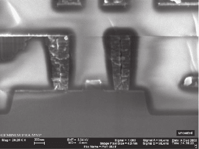
shown in Figure 3–30. Figure 3–47 shows the cross-fractured semicon-
ductor structure with Schottky barrier on tungsten contacts. A nano-
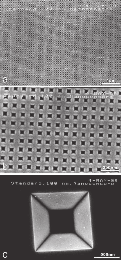
structured two-dimensional lattice of 100-nm spaced inverted square
pyramids in silicon used as standard for scanning probe microscopy
is shown in Figure 3–48. Imaging of the uncoated lattice is necessary
to avoid modifi cations of the standard by thin fi lm coating, thus LVSEM
is most appropriate.
Another challenging application for LVSEM is the quantitative char-
acterization of the geometry and radius of very sharp tips for atomic
force microscopy, which are necessary for many quantitative measure-
ments with the AFM (e.g., Fruhsdorfer et al., 2002; Matzelle et al., 2000,
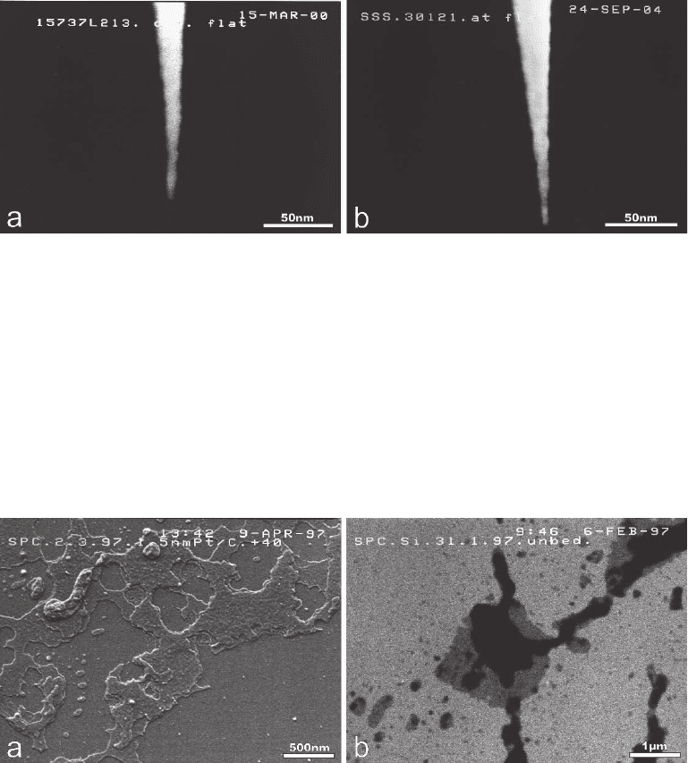
2003). Figure 3–49 shows two extremely sharp commercial tips. The
tip radius at the very end amounts typically to 2–3 nm, thus only SE1
contribute to the signal. An optimum quality of SE imaging in terms
of sharpness, contrast, and SNR can be obtained with electron energies
ranging from about 3 to 10 keV. It seems worth mentioning that very
sharp tips are interesting samples with which to study experimentally
the delocalization of the secondary electrons.
The characterization of organic mono- and multilayers on solids is
especially valuable in technology development, such as bio- and che-
mosensors, since detailed information on the fi lm surface and its mor-
phology is obtained. Figures 3–50 to 3–53 demonstrate with different
mono- and multilayered ultrathin uncoated and coated organic fi lms
how direct information about the fi lm thickness, step heights of the
fi lm, and differences in the “chemistry” and molecular packing density
can be obtained. As shown by Figure 3–50a, upward and downward
steps with height differences of a few nanometers can be readily
Figure 3–47. Secondary electron micrograph (“through-the-lens” detection)
of a cross-fractured semiconductor structure with Schottky barrier on tung-
sten contacts. The image was recorded at 3.04 kV. The cross-fracture reveals
the interior features and the potential barrier of 0.6 eV (dark due to voltage
contrast). (Courtesy of Carl Zeiss NTS, Oberkochen, Germany.)
228 R. Reichelt
Figure 3–48. Secondary electron micrographs of an uncoated 100-nm calibra-
tion standard made from silicon for scanning probe microscopy (NANO-
WORLD, Neuchatel, Switzerland) recorded with an “in-lens” fi eld emission
SEM at 3 kV. The calibration standard consists of a two-dimensional lattice
(lattice constant = 100 nm) of inverted pyramids shown at different magnifi ca-
tions (a and b). (c) Structural details of a large pyramidal pit.
Chapter 3 Scanning Electron Microscopy 229
Figure 3–49. Secondary electron micrographs of uncoated SuperSharpSilicon AFM Probe silicon
cantilevers for noncontact/tapping mode (NANOWORLD, Neuchatel/Switzerland) in atomic force
microscopy recorded with an “in-lens” fi eld emission SEM at 3 kV (a) and at 10 kV (b). The tip radius
of both tips amounts to about 2–3 nm.
Figure 3–50. Secondary electron micrographs of a phospholipid/protein fi lm [dipalmitoylphosphati-
dylcholine (DPPC):dipalmitoylphosphatidylglycerol (DPPG) (ratio = 4 : 1)/pulmonary surfactant
protein C (SP-C; 0.4 mol%)] supported by a silicon wafer. The organic fi lm has terrace-like regions of
different thickness (height differences between terraces are between 5.5 and 6.5 nm (von Nahmen et
al., 1997). Micrographs were recorded with an “in-lens” FESEM at 2 keV from the ultrathin platinum/
carbon-coated fi lm (tilted 40° around the horizontal axis) (a) and at 1.8 keV from the uncoated fi lm (b).
[Specimens kindly provided by Dr. H.-J. Galla and Dr. M. Siebert, Institut für Biochemie, University
of Münster, Münster, Germany.)
230 R. Reichelt
0
0
200
400
600
Å
0.5 1 1.5
2 µm
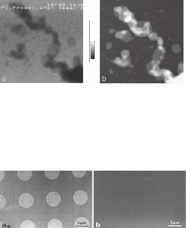
Figure 3–51. Secondary electron micrograph (a) and AFM topography (b) of the same area of an
uncoated phospholipid/protein fi lm [dipalmitoylphosphatidylcholine (DPPC):dipalmitoylphosphati-
dylglycerol (DPPG) (ratio = 4 : 1)/pulmonary surfactant protein C (SP-C; 0.4 mol%)] supported by a
silicon wafer. The organic fi lm has terrace-like regions of different thickness [height differences
between terraces are between 5.5 and 6.5 nm (von Nahmen et al., 1997)]. The micrograph was recorded
with an “in-lens” FESEM at 2 keV. The scale inbetween (a) and (b) represents the coding of brightness
relative to the height used in the topograph (b). (Specimens kindly provided by Dr. H.-J. Galla & Dr.
M. Siebert, Institut für Biochemie, University of Münster, Münster, Germany.)
Figure 3–52. Secondary electron micrographs of a patterned self-assembled thiol monolayer on poly-
crystalline gold recorded at 2 keV with the “in-lens” FESEM. (a) Uncoated monolayer. The circular
domains consist of —S(CH
2
)
15
CH
3
molecules (hydrophobic), which are surrounded by —S(CH
2
)
12
OH
molecules (hydrophilic). The contrast is due to the different end groups rather than to the small dif-
ference in chain length. (b) Monolayer coated with an ultrathin platinum/carbon fi lm. (Specimen
kindly provided by Dr. G. Bar, Freiburger Material Forschungszentrum, Freiburg, Germany.)
Chapter 3 Scanning Electron Microscopy 231
LC-phase, uncoated area
Å
Å
40.0
20.0
0.0
1200
800
400
0
LE-phase, uncoated area
Pt/C-coated area
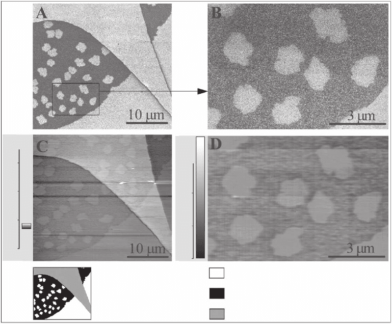
Figure 3–53. Secondary electron micrographs (A and B) and AFM topographs (C and D) of the same
area of a 1,2-dipalmitoyl-sn-glycero-3-phosphothioethanol (DPPTE) monolayer on a silicon wafer
having domains with densely [liquid condensed (LC) phase] and losely [liquid expanded (LE) phase]
packed molecules. The specimen was masked by a TEM fi nder grid and then coated with an ultrathin
platinum/carbon fi lm to obtain neighboring coated and uncoated areas on the specimen (for details
see Bittermann et al., 2001). The SE micrographs were recorded with an “in-lens” FESEM at 5 keV. The
brighter regions of the SE micrograph (B) correlate with the elevated domains (LC phase) in the AFM
topograph (D), whereas the darker regions correlate with the LE phase. In contrast to the SE micro-
graph (A) the height differences in coated areas of the fi lm, which are related to its molecular packing
density, are still visible in the AFM topograph (C). [From Bittermann et al. (2001); with kind permis-
sion of the American Chemical Society, Columbus, OH.]
232 R. Reichelt
identifi ed on a tilted sample coated with an ultrathin con ductive fi lm.
Whereas the step of constant height reveals in an “in-lens” SEM a
constant intensity at normal electron beam incidence, tilting causes an
asymmetry such that steps can face upward or downward, which leads
to an increase or decrease of their image intensities, respectively.
Uncoated organic layers on solids usually reduce the SE yield as shown
in Figure 3–50b. As demonstrated in Figure 3–51 by a comparison of
an SE micrograph with an AFM topograph of the same area, the SE
intensity decreases with increasing thickness of the organic layer
(Reichelt, 1997). The monotonic dependence of SE intensity and the
thickness of the organic fi lm enables its thickness to be mapped without
destruction of the fi lm. The infl uence of organic fi lm thickness on the
SE yield vanishes after ultrathin coating of the organic fi lm as proven
by Figure 3–50a.
Figure 3–52a demonstrates that the SE yield also depends on the
chemical nature of the molecules assembling an organic fi lm. For
example, differences in the terminal group of molecules obviously
cause a signifi cant difference in the SE yield, which creates a suffi cient
chemical contrast in the micrograph. This chemical contrast vanishes
after ultrathin coating of the organic fi lm (Figure 3–52b). Finally, Figure
3–53 shows that the SE yield is sensitive to the molecular packing
density of the organic fi lm, i.e., the number of organic molecules per
area (Bittermann et al., 2001).
It is easy to understand that the BSE signal is not sensitive to the fi lm
thickness and differences in the “chemistry” and molecular packing
density, because the backscattering of thin low atomic number fi lms is
negligible compared with those of the substrate having a signifi cantly
higher atomic number.
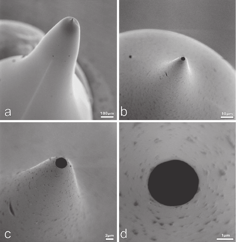
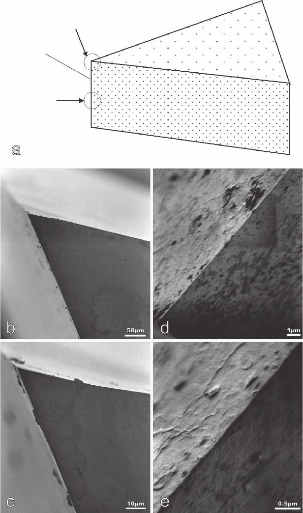
Figures 3–54 and 3–55 show secondary electron micrographs of an
uncoated glass micro pipette and a microtome glass knife, which are
almost free of electric charging. However, at higher magnifi cations the
typical signs of charging occur.
The characterization of sponge-like microstructures, such as hydro-
gels and microgels, is a further challenging application of LVS EM,
where a large depth of focus, high resolution, and low pene tration
power (i.e., small electron range) of the electron beam are required.
Figure 3–56 shows a stereopair of highly magnifi ed SE micrographs of
a hydrogel. The optimum imaging quality of fi ne structural details
well below 10 nm was obtained with electron energies around 2 keV.
Figures 3–57 and 3–58 show a set of secondary electron micrographs
recorded from biological samples at low magnifi cation with different
electron energies. The micrographs demonstrate to what extent the
contrast and information depth vary with the electron energy in a
range from 0.4 to 30 keV, which corresponds to about the accessible
energy range of commercial FESEMs. As yet, not all of the contributing
contrast mechanisms are fully understood, thus the interpretation
of micrographs recorded at a specifi c selected energy requires great
care.
Finally, LVSEM is also a promising and effi cient alternative to con-
ventional approaches for micromorphological and microstructural
Chapter 3 Scanning Electron Microscopy 233
Figure 3–54. Secondary electron micrograph series (a–d) of increasing magnifi cation of an uncoated
glass micropipette recorded at 2 kV with an “out-lens” FESEM. The uppermost part of the tip of the
micropipette is within the depth of focus. The lower part is out of focus.
234 R. Reichelt
Cutting
edge
d,e
b,c
Figure 3–55. Scheme and SE micrographs of an uncoated microtome glass knife recorded at 1 kV with
an “out-lens” FESEM. The arrows in (a) indicate the two directions of the electron beam related to the
glass knife, which were used for imaging. (b and c) The electron beam has a shallow angle against
the cutting edge. Only the uppermost part of the cutting edge is within the depth of focus. (d and e) The
electron beam impinges perpendiculary onto the cutting edge. The different mean brightness of the
clearance angle side and backside of the knife is due to the effect of the detection geometry of the ET
detector.
