Hawkes P.W., Spence J.C.H. (Eds.) Science of Microscopy. V.1 and 2
Подождите немного. Документ загружается.

Chapter 3 Scanning Electron Microscopy 135
having a partial pressure in the low vacuum range mentioned. Typical
examples are water or oil containing natural specimens. Moreover,
electric insulators can be imaged without prior conductive coating by
ESEM in low vacuum without signifi cant electric charging artifacts.
The ESEM (ESEM is used as a trade name by the manufacturers
Electroscan/Philips/FEI) became commercially available in 1987 (for
reviews of specifi c aspects of the instrumentation, image formation,
and application of ESEM see, e.g., Danilatos, 1988, 1990). Since about
the second half of the 1990s other manufacturers also offer commercial
SEMs for low vacuum operation, usually referred to as low vacuum
SEM, variable pressure SEM, natural SEM, etc.; however, these instru-
ments are restricted typically to a maximum pressure of about 300 Pa
and allow imaging only with backscattered electrons (BSE).
Modern high-resolution FESEMs have at an electron energy of 30 keV
a specifi ed resolution power in the SE mode in the range of 0.5–1 nm,
which corresponds to about the size of a small molecule. It marks the
smallest size of a structure accessible on one hand. Working at the
smallest magnifi cation of an SEM on the other hand allows imaging of
visible structures as large as about 1 mm, i.e., high-resolution SEMs
cover a wide range of six orders of magnitude for the structural char-
acterization of surfaces. A further advantage of the SEM is the simul-
taneous acquisition of different signals generated by the local interaction
of the beam electrons with the specimen. Each of these signals, e.g., SE
and BSE, carries different information about the sample, thus an exten-
sive multidimensional data set about an area of interest can be obtained
by one scan line-by-line across this area. The recording time may vary
from a few seconds only to about 1 min depending on the strength of
the signal and the signal-to-noise ratio required.
The scanning electron microscopy is now a well-established method
for the characterization of surfaces in ultrahigh vacuum (UHV), high
vacuum (HV), and low vacuum (LV) in many different fi elds. Clearly,
it is not possible to mention all of them, however, the main fi elds are
certainly the materials (metals, alloys, ceramics, glasses) and surface
sciences, semiconductor research and industry, life sciences, and mis-
cellaneous sciences such as polymer and food research, mineralogy,
geology, the oil industry, and archaeology.
In addition to scanning electron microscopy some other surface-
sensitive methods such as atomic force microscopy, scanning tunnel-
ing microscopy, and photoelectron microscopy are described in the
book “Science of Microscopy.” It is certainly of particular interest to
see in detail how these surface-sensitive methods complement each
other, what specifi c advantages they offer, and how they compare with
SEM.
1.1 Abbreviations
ADC Analog-to-digital-converter
AE Auger electrons
AES Auger electron spectroscopy
136 R. Reichelt
AFM Atomic force microscope/microscopy
ASEM Atmospheric scanning electron microscope/
microscopy
CC Charge collection
CE Collection effi ciency
CFEG Cold fi eld emission gun
CRT Cathode ray tube
CSEM Conventional high vacuum scanning electron
microscope/microscopy
EBIC Electron beam-induced current
EBSD Electron backscattered diffraction
ECP Electron channeling pattern
EDX Energy dispersive X-ray
ESEM Environmental scanning electron
microscope/microscopy
ET Everhart–Thornley
ETD Everhart–Thornley detector
FEG Field emission gun
FESEM Filed emission scanning electron
microscope/microscopy
FLM Fluorescence light microscopy
HFEG Hot fi eld emission gun
HRSEM High-resolution scanning electron
microscope/microscopy
HV High vacuum
LCD Liquid crystal display
LEED Low-energy electron diffraction
LP Light pipe
LV Low vacuu m
LVSEM Low-voltage scanning electron microscope/microscopy
MCP Microchannel plate
MEMS Microelectromechanical systems
NEMS Nanoelectromechanical systems
OIM Orientation imaging microscopy
PC Personal computer
CL Cathodoluminescence
Chapter 3 Scanning Electron Microscopy 137
SAM Scanning Auger microscopy
SE Secondary electrons
SEC Schottky emission cathode
SEM Scanning electron microscopes
SLEEM Scanning low-energy electron microscope/microscopy
S/N Signal to noise
SNR Signal-to-noise ratio
STEM Scanning transmission electron microscope/
microscopy
STM Scanning tunneling microscope/microscopy
UHV Ultrahigh vacuum
UV Ultraviolet
VLVSEM Very low-voltage scanning electron microscopy
WD Work distance
WDX Wavelength dispersive X-ray
YAG Yttrium-aluminum-garnet
YAP Yttrium-aluminum-perovskite
3D Three dimensional
1.2 Symbols
A Atomic weight
C
c
Chromatic aberration constant
C
s
Spherical aberration constant
d Lattice-plane spacing
d
p
Final electron probe diameter d
p
at the specimen
d
pe
Effective fi nal electron probe diameter
d
p,min
Minimum effective electron probe diameter
d
c
Diameter of the error disc of chromatic aberration
d
f
Diameter of the diffraction caused Airy disc
d
s
Diameter of the error disc of spherical aberration
d
o
Diameter d
o
of the fi rst crossover
E Electron energy
E
AE
Energy of Auger electrons
E
o
Electron energy of the beam electrons
138 R. Reichelt
E
BSE
Energy of backscattered electrons
E
2
Beam electron energy where the number of incoming and
emitted electrons is equal
E
X
X-ray energy
E
exm
Mean energy per excitation of an electron hole pair
F Flux of gas molecules
f Focal length of a lens
I
CC
Charge-collection current
I
p
Electron probe current
I
p,max
Maximum electron probe current
j
c
Current density for thermionic emission
J Mean ionization potential
L Electron path length in gas
N Number of atoms per unit volume
N
A
Avogadro’s number
N ⋅ I Ampere-windings of an electromagnetic lens
n
m
Mean number of electron hole pairs
M Magnifi cation
p Object distance to the center of the lens
p
g
Pressure in the specimen chamber of the SEM
p
x
Parallax
q Image distance to the center of the lens
R Electron range
R
B
Bethe range
T Temperature
t Specimen thickness
Z Atomic number
α
p
Semiangle of the convergent impinging electron probe at the
specimen
α
opt
Optimum value of α
p
∆E Energy spread of the beam electrons
Φ Work function
θ Angle of incidence of the electron beam
Θ Tilt angle of the specimen
ϕ Scattering angle
Chapter 3 Scanning Electron Microscopy 139
ϑ Bragg angle
α
o
Semiangle of divergence of the fi rst crossover
δ Secondary electron yield
η Backscattered electron coeffi cient
λ Wavelength of the beam electrons
λ
x
Wavelength of X-ray
Λ Mean free path for electron scattering in gas
Λ
el
Mean free path for elastic scattering
Λ
in
Mean free path for inelastic scattering
σ Electron scattering cross section
σ
el
Elastic electron scattering cross section
σ
in
Inelastic electron scattering cross section
σ
g
Total electron scattering cross section of gas molecule
ε Complex dielectric constant
ε
0
Dielectric constant
ν Frequency of radiation
ω Fluorescence yield of X-rays
2 Conventional Scanning Electron Microscopy
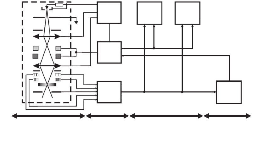
The principle of a scanning electron microscope is shown schematically
in Figure 3–1. The two major parts are the microscope column and the
electronics console. The microscope column consists of the electron gun
(with the components cathode, Wehnelt cylinder, anode), one or two
condenser lenses, two pairs of beam defl ection coils (scan coils for X, Y
defl ection), the objective lens, and some apertures. In the specimen
chamber at the lower end of the microscope column are located the
specimen stage and the detectors for the different signals generated by
the electron–specimen interaction. The microscope column and the
specimen chamber are evacuated using a combination of prevacuum
and high vacuum pumps (usually oil diffusion pumps). The pressure
in the specimen chamber typically amounts to about 10
−4
Pa, allowing
the beam electrons to travel from the cathode to the specimen with little
interaction with the residual gas molecules. The electronics console
consists of the electric power supplies for the acceleration voltage (usual
range about 0.5–30 kV) as well as the condenser and objective lenses, the
scan generator, and electronic amplifi ers for the different signals
acquired. Moreover, the console also houses one or more monitors
[cathode ray tube (CRT) or liquid crystal display (LCD)] for displaying
the micrograph(s), a photo-CRT for analogous image recording, and
numerous knobs and a computer keyboard to control the electron

140 R. Reichelt
beam, the signals selected, and the image recording. Now modern
SEMs mostly use a PC to control the electron beam, to select the signals,
and to record as well as to store the digital image(s). In that case the
numerous knobs are obsolete and are replaced by a mouse-controlled
interactive program running on the PC.
How does the SEM work? The beam electrons are emitted from the
cathode and accelerated by a voltage of 0.5–30 kV between the cathode
and anode forming a smallest beam cross section—the crossover—near
the anode with a diameter of about 10–50 µm. This spot size is too large
to produce a sharp image. Therefore the crossover is demagnifi ed by
the lens system consisting of one or two condenser lenses and one
objective lens and focused on the specimen surface. Most SEMs can
produce an electron beam having a smallest spot size of about 5–10 nm
and an electron probe current in the range of 10
−12
–10
−10
A, which is
suffi cient to form an image with a reasonable signal-to-noise (S/N)
ratio. For higher probe currents required for some modes of operation
the smallest probe spot size increases to 100 nm or more. The objective
lens has a variable relatively long focal length that allows a large
c
w
A
ConA
ConL
Defl. X,Y
Defl. X,Y
OL
OA
Det.
DF-D
Microscope column
Specimen chamber
Detectors
Electronics Image display
Photography
Accelerating
voltage
+
Lens
currents
Scan
generator
Amplifier
SE
BSE
STEM
CL
X-ray
PC
Monitor
Photo-Monitor
Digital scan
Digital image
Acquisition & storage
Image display
Image processing
Figure 3–1. Schematic drawing of a conventional SEM. The evacuated microscope column (inside the
bold dashed frame) contains the electron gun, electromagnetic lenses, electromagnetic defl ection coils,
apertures, the specimen stage, and the detectors. The electronics console houses the power supplies
for the acceleration voltage and the electromagnetic lenses, the scan generator, amplifi ers for the
signals, and monitors for display and recording of images. Modern SEMs are controlled by a PC. A,
anode; BSE, backscattered electrons; C, cathode; ConA, condenser aperture; ConL, condenser lens; CL,
cathodoluminescence; Defl . X, pair of beam defl ection coils in the X direction; Defl . Y, pair of beam
defl ection coils in the Y direction; Det., detectors; DF-D, dark-fi eld detector; O, specimen; OA, objective
aperture; OL, objective lens; PC, personal computer; SE, secondary electrons; STEM, scanning trans-
mission electron microscope signal; W, Wehnelt cylinder; X-ray, X-ray signal.
O

Chapter 3 Scanning Electron Microscopy 141
working distance (WD; it corresponds to the distance between the
specimen and lower pole piece) in the range of about 5–30 mm. This
ensures that the various signals generated by the impinging beam
electrons (Figure 3–2) in the small specimen interaction volume can be
collected by detectors located lateral above the specimen with suffi cient
effi ciency. Pairs of beam defl ection coils located in front of the objective
lens and controlled by a scan generator scan the electron probe line by
line across a small area of the specimen. Simultaneously, the scan gen-
erator controls the defl ection coil system of a monitor. The intensity of
the monitor is modulated by the amplifi ed signal selected by the
operator.
The signals may vary from one location to another as the electron–
specimen interaction changes due to, e.g., topography and specimen
composition. The magnifi cation of the image is given by the ratio of
the length of the scan on the monitor and the corresponding length of
the scan on the specimen. For example, an increase in magnifi cation
can simply be achieved by decreasing the current of the defl ection coils
in the microscope column (i.e., lowering the length of the scan on the
specimen) and keeping the image size on the monitor constant. It
should be mentioned that the magnifi cation also depends on the WD,
however, modern SEMs compensate automatically for each WD, thus
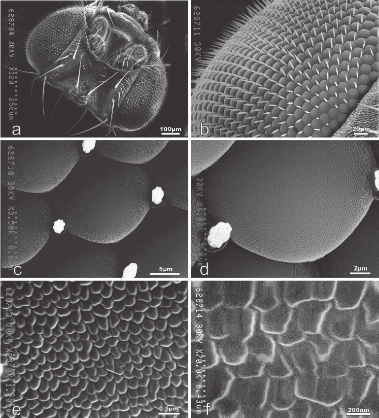
keeping the displayed magnifi cation correct. Figure 3–3 shows a series
of images recorded with increasing magnifi cations over a range of
almost three orders of magnitude.
For crystal structure analysis (cf. Section 7) basically two strategies
exist: (1) The mode of beam defl ection changes from scanning line by
line to rocking of the electron beam when the probe is at rest on a
chosen location and the angle of incidence is scanned within a select-
Primary electrons
E
0
= 0.1 - 30 keV
Cathodoluminescence / X-rays
hν <E
0
Backscattered electrons
50eV < E ≤ E
0
Secondary electrons
E ≤ 50eV
Specimen
Elastically
scattered
electrons
E = E
0
Unscattered
electrons
E
0
Inelastically
scattered
electrons
E = E
0
- E
Auger electrons
E = E
AE
∇
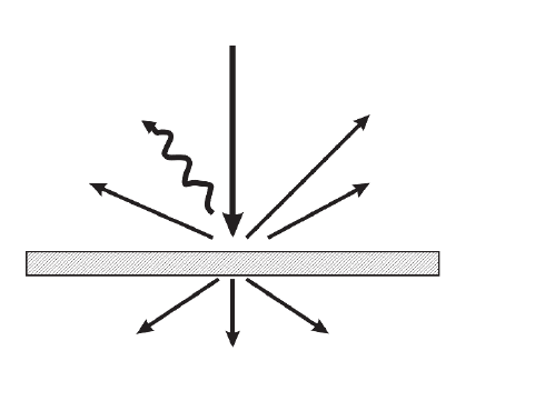
Figure 3–2. Schematic drawing of signals for a thin sample generated by the
impinging electrons. E
O
, energy of beam electrons; E, energy of signal elec-
trons; E
AE
, energy of Auger electrons; ∆E, energy loss of inelastically scattered
electrons; hν, energy of radiation.

142 R. Reichelt
able angular range to form an electron channeling pattern. (2) The
electron backscattered diffraction pattern from the point of electron
beam impact is recorded by means of a position-sensitive detector and
analyzed revealing information about the local crystal structure.
One of the greatest strengths of the SEM is the tremendous depth of
focus, i.e., the range of heights of the specimen being simultaneously
in focus (cf. Figure 3–3). Due to the small objective aperture diaphragm
(about 50–100 µm) and the large WD the semiangle α
p
of the convergent
Figure 3–3. Micrograph series of increasing magnifi cation of the head and the eye of a fl y (Drosophila
melanogaster), recorded with secondary electrons at 30 kV. The specimen was air dried and sputter
coated with about 15 nm gold. Note the large depth of focus. The last magnifi cation step from (e) to
(f) barely reveals further fi ne details of the specimen because of the preparation used. The scale of
dimensions of the micrographs covers about three orders of magnitude.

Chapter 3 Scanning Electron Microscopy 143
impinging electron probe is in the order of 10 mrad only. At magnifi ca-
tions that are comparable to those of light microscopy (e.g., 1000×) the
SEM has a depth of focus that is about 100 times greater than that of
an optical microscope, obviously because the semiangle of convergence
is much larger in the latter case.
To take full advantage of all the information that SEM can provide,
an understanding of its operation modes and the infl uence of electron
beam parameters on the image resolution, the image contrast, the
signal strength, and the S/N ratio as well as the electron–specimen
inter action is mandatory. The remarkable success of scanning electron
microscopy over several decades is mainly due to the tremendous
depth of focus, the brilliant image contrast, and the relatively straight-
forward sample preparation for imaging of surfaces, and, in combina-
tion with X-ray microanalytical equipment, its capability of local
quantitative element analysis of specimens.
2.1 Electron Guns, Electron Lenses, Detectors, and Stages
2.1.1 Electron Guns
The electron gun provides the SEM with an electron beam of adjustable
current and energy. The most classic electron gun is the triode gun
based on thermionic emission from a tungsten fi lament heated to about
T
c
= 2700 K (cf. Figure 3–4). The fi lament has a diameter of about 0.1 mm
and is bent in the shape of a V hairpin to localize the emission area on
the tip. The size of this area is around 100 × 150 µm. By ther mionic
excitation the electrons overcome the work function Φ of the tungsten
tip and a current with the density j
c
is emitted according to the
Richardson law
j
c
= AT
c
2
exp(−Φ/kT
c
) (2.1)
Cathode
Wehnelt
Crossover
Anode
U =
1-50 kV
–
+
R
W
U
W
U
H
I
c
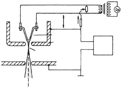
Figure 3–4. Schematic drawing of the thermionic emission triode gun with a
tungsten hairpin fi lament. The fi lament is heated by the applied voltage U
H
.
R
w,
variable resistor to adjust the potential U
W
between the Wehnelt cylinder
and cathode; U, acceleration voltage. [Adapted from Reimer (1993); with kind
permission of the International Society of Optical Engineering (SPIE), Belling-
ham, WA.]
144 R. Reichelt
where A represents a constant depending on the cathode material and
k is the Boltzmann constant; Φ = 4.5 eV for tungsten. The density j
c
depends strongly on the temperature: j
c
is about 1.8 A cm
−2
for T
c
=
2700 K and about 3 A cm
−2
for T
c
= 2800 K.
The emitted electrons are accelerated from the fi lament at a high
negative potential (e.g., −30 kV) toward the anode at ground potential
(0 V). Central holes in the Wehnelt cylinder and in the anode enable a
fraction of the accelerated electrons (e.g., E
o
= 30 keV) to move toward
the lenses in the microscope column. The emission current is typically
in the order of 100 µA and can be controlled by the bias of the Wehnelt
cylinder, which surrounds the fi lament. The negative Wehnelt bias is
provided by a voltage drop caused by the emission current through the
resistor R
W
. The electrostatic fi eld distribution inside the triode gun has
a focusing action to the emitted electrons generating a crossover that is
located between the Wehnelt cylinder and the anode. This crossover
can be characterized by the diameter d
o
and the semiangle α
o
of the
divergence. d
o
is usually in the order of 50 µm. As we will see later the
condenser and objective lenses produce a demagnifi ed image of that
crossover on the specimen surface representing the fi nal electron probe
(diameter d
p
).
An important parameter of an electron gun is its axial brightness β,
which is defi ned as the beam current per area (equal to current density)
into a solid angle πα
2
(Reimer, 1985)
β = j/πα
2
= const. (2.2)
It is important to note that the brightness remains constant for all
points along the electron optical axis from the cathode through the
microscope column to the specimen. This means that the brightness of
the fi nal electron probe on the specimen surface is equal to the bright-
ness of the gun regardless of apertures in the microscope column,
i.e.,
β = 4I
o
/π
2
d
o
2
α
o
2
= 4I
p
/π
2
d
p
2
α
p
2
(2.3)
where I
o
is the beam current at the crossover inside the electron gun.
Equation (2.3) shows that the characteristic illumination parameters I
p
,
d
p
and α
p
cannot be changed independently. For example, an increase
of β for given d
p
and α
p
clearly requires an increase of I
p
.
The work function of tungsten is relatively high. Lanthanum hexa-
boride (LaB
6
) has a signifi cantly lower work function (Φ = 2.7 eV) and
can therefore emit greater current densities at lower temperature (T
c
=
1900 K). At the same time the brightness of the electron probe is also
increased since the maximum brightness of an electron gun (Reimer,
1985) is given as
β = j
c
E
o
/πk T
c
(2.4)
i.e., the brightness β is inversely proportional to the temperature of the
cathode. The LaB
6
cathode consists of a small piece of an LaB
6
single
crystal with a tip radius typically of about 1 µm. The single crystal is
supported by a nonreactive material and is resistively heated. It seems
worth mentioning that (1) in the cathode chamber the operation of an
