Hawkes P.W., Spence J.C.H. (Eds.) Science of Microscopy. V.1 and 2
Подождите немного. Документ загружается.

1070
17
Low-Temperature Scanning
Tunneling Microscopy
Uwe Weierstall
1 Introduction
The scanning tunneling microscope (STM) has revolutionized surface
science since its invention in 1982 (Binnig and Rohrer, 1982) by provid-
ing a means to directly image atomic scale spatial and electronic
structure. Using the combination of a coarse approach and piezoelec-
tric transducers, a sharp, metallic tip is brought into close proximity
with the sample. The distance between tip and sample is less than
1 nm, which means that the electron wave functions of tip and sample
start to overlap. A bias voltage is applied between tip and sample that
causes electrons to tunnel through the barrier. The tunneling current
is a quantum mechanical effect: tunneling of electrons can occur
between two electrodes separated by a thin insulator or a vacuum
gap and the tunneling current decays on the length scale of one
atomic radius. The tunneling current is in the range of picoamperes
to nanoamperes and is measured with a preamplifi er. In an STM, the
tip is scanned over the surface and electrons tunnel from the very
last atom of the tip apex to single atoms on the surface, providing
atomic resolution. The exponential dependence of the tunneling
current on the tip–sample distance can be exploited to control the
tip–sample distance with high precision. There are four basic opera-
tion modes for any STM: constant current imaging, constant height
imaging, spectroscopic imaging, and local spectroscopy. Their inter-
pretation and realization will be briefl y discussed below. For details
about other modes and a comprehensive introduction to electron tun-
neling and STM see Wiesendanger (1994).
To acquire constant current images, a feedback loop adjusts
the height of the tip during scanning so that the tunneling current
fl owing between tip and sample is kept constant. The height z is
adjusted by applying an appropriate voltage V
z
to the z-piezoelectric
drive while the lateral tip position (x,y) is determined by the
corresponding voltages applied to the x and y piezoelectric drives.
The recorded signal V
z
can be translated into a topography z(x,y)
if the sensitivity of the piezoelectric drives is known. The word
Chapter 17 Low-Temperature Scanning Tunneling Microscopy 1071
topography should be used with caution: since the local density of
states at the Fermi level is measured, a molecule adsorbed on a metal
surface that reduces the local density of states and may actually be
imaged as a depression.
To acquire constant height images, the feedback loop is switched off,
i.e., the tip is scanned at constant height above the surface, and varia-
tions in the current are measured. This mode has the advantage that
the fi nite response time of the feedback loop does not limit the scan
speed. It can be used to collect images at video rates, offering the
opportunity to observe dynamic processes at surfaces. However,
thermal drift limits the time of the experiment and there is an increased
risk of crashing the tip.
To measure differential conductance (dI/dV) maps with the STM, a
high-frequency sinusoidal modulation voltage is superimposed on the
constant dc bias voltage V
bias
between tip and sample. The modulation
frequency is chosen higher than the cutoff frequency of the feedback
loop, which keeps the tunneling current constant. By recording the
tunneling current modulation, which is in phase with the applied bias
voltage modulation, with a lock in amplifi er, a spatially resolved spec-
troscopic signal dI/dV|
V
bias
can be obtained simultaneously with the
constant current image (Binnig et al., 1985a,b).
By measuring the differential conductance dI/dV at a fi xed tip posi-
tion with open feedback loop (constant tip–sample distance z) while
sweeping the applied bias voltage, an energy-resolved spectrum can
be obtained. This is useful for probing, e.g., band-gap states in semi-
conductors or the onset of surface states on metals.
The tunneling current I at a given tip position is approximately equal
to the integrated local density of states (ILDOS), integrated over the
energy range between the Fermi energy E
F
of the sample and eV, where
V is the applied bias voltage. Therefore the differential conductance
dI/dV is approximately proportional to the local density of states
(LDOS) of the sample at the energy eV, and a constant current image
should represent a contour of constant ILDOS. For measurements close
to E
F
, i.e., at low bias voltages, the LDOS and ILDOS are essentially the
same and a constant current image at low bias (a few millivolts) is
therefore approximately proportional to the sample LDOS at the Fermi
energy E
F
(assuming the tip has a uniform density of states and the
temperature is low). To illustrate how to arrive at the picture presented
above, the theoretical treatment of electron tunneling is briefl y
outlined.
A one-dimensional WKB approximation predicts that the tunneling
current at low temperatures (where the Fermi distribution is a step
function) is given by
IExeVExTEeVxdE
eV
=
(
)
−+
(
)
(
)
∫
ρρ
st
,,,,
0
(1)
where ρ
s
(E) and ρ
t
(E) are the density of states of the sample and the tip
at the location x and energy E, measured with respect to their individ-
ual Fermi levels, and V is the applied bias voltage (Hamers, 1989). The

1072 U. Weierstall
tunneling transmission probability T(E,eV,x) for electrons with energy
E and applied voltage V is given by
TEeVx zx
m
eV E,,
ts
(
)
=−
(
)
++ −
(
)
exp
4
2
2
φφ (2)
where φ
s
and φ
t
are the work functions of sample and tip and z is the
tip–sample distance. Therefore, assuming that the tip electronic struc-
ture is featureless, Eq. (1) shows that the tunneling current at position
x is approximately equal to the ILDOS of the sample integrated between
E
F
and eV, weighted by the transmission probability T. Examination of
Eq. (2) shows that if eV < 0 (i.e., negative sample bias), the transmission
probability is largest for E = 0 (corresponding to electrons at the Fermi
level of the sample). If eV > 0 (positive sample bias) the probability is
largest for E = eV (corresponding to electrons at the Fermi level of the
tip). Therefore the tunneling probability is always largest for electrons
at the Fermi level of whichever electrode is negatively biased. This is
shown schematically in Figure 17–1.
Differentiating Eq. (1) gives the differential conductance
dI
dV
eV x x T eV eV x
Ex E e
∝
(
)
(
)
(
)
+
(
)
−
ρρ
ρρ
st
st
,, ,,
,
0
VVx
dT E eV x
dV
dE
eV
,
,,
(
)
(
)
∫
0
(3)
The fi rst term is the product of the density of states of the sample,
the density of states of the tip, and the tunneling transmission pro-
bability. The second term contains the voltage dependence of the
tunneling transmission probability. Since T is a smooth monotonically
Figure 17–1. Energy level diagram of sample and tip with V being the sample
voltage relative to the tip. Left: electrons tunneling from tip to sample with
positive sample bias voltage. Right: electrons tunneling from sample to tip
with negative sample bias voltage. The curve represents the density of states
of the sample; the tip density of states is assumed featureless. The different
lengths of the arrows illustrate the fact that the tunneling probability is largest
for electrons at the Fermi level of the negatively biased electrode. Φ
t
and Φ
s
are
the tip and sample work functions.
eV>0 eV<0
s
t
t
E
F
s
eV
E
F
E
F
eV
E
F
sample
tip sample tip
Chapter 17 Low-Temperature Scanning Tunneling Microscopy 1073
increasing function of V, structure in dI/dV can be assigned to changes
in the sample LDOS at eV, assuming a tip with featureless density of
states.
In general, however, the tip electronic structure is unknown and may
not be featureless. The small size of the STM tip is expected to signifi -
cantly modify its electronic structure from that of a bulk material.
Therefore, it is usually necessary to compare tunneling spectra acquired
at different locations on the surface to distinguish the spatially invari-
ant contribution of the tip and the spatially varying contribution from
the sample. Comparing spectra taken with different tips also helps to
eliminate tip contributions.
At fi nite temperatures Eq. (1) contains an additional Fermi distribu-
tion factor, which imposes a limit on spectroscopic resolution. At room
temperature, with k
B
T ≈ 0.026 eV, the spread of the tip and sample
energy distribution are each 2 k
B
T ≈ 0.052 eV. Therefore the total spread
is ∆E ≈ 4 k
B
T ≈ 0.1 eV. To make high-resolution spectroscopic measure-
ments with ∆E in the millielectron volt range, experiments must be
conducted at cryogenic temperatures.
To work with clean metal and semiconductor surfaces, STM mea-
surements have to be done in ultrahigh vacuum (UHV). Operating a
UHV-STM at cryogenic temperature has several major advantages:
1. Close coupling of the microscope to a large temperature bath that
keeps constant temperature over hours or days ensures a reduction of
thermal drift and allows long-term measurements. The reduction of
thermal drift during low-temperature operation is further improved
by the fact that the thermal expansion coeffi cients at liquid helium
temperature are two or more orders of magnitude smaller than at room
temperature.
2. Superior vacuum conditions: If the microscope is incorporated in
a cryostat that acts as an effective cryopump, surfaces are kept free
from contamination over days.
3. Thermal diffusion of adsorbates and defects is suppressed—stable
imaging becomes possible even for weakly bound species. Moreover,
low temperatures might also stabilize the atomic confi guration at the
tip end by preventing sudden jumps of the most loosely bound fore-
most atoms due to thermal activation.
4. Small thermal broadening at the Fermi energy is a necessary
condition for spectroscopic investigations with high-energy
resolution.
5. Individual adsorbates can be manipulated with the STM to quali-
tatively probe their interaction with the substrate.
6. Physical properties can be studied as a function of temperature
or physical effects can be examined that occur only at low temperatures
(e.g., superconductivity, Kondo effect, nanoscale magnetism).
7. Piezo non l i nea rit ies and hysteresis (creep) affecting the piezoelec-
tric scanners of the STM decrease substantially at low temperatures.
In an effort to improve the stability of the microscope and the atoms
or molecules under investigation, a variety of low-temperature UHV
STM designs have been developed.
1074 U. Weierstall
2 Design Principals
All low-temperature STMs (LT-STM) operate in UHV, which is a pre-
requisite for obtaining a clean surface. To reach a low fi nal tempera-
ture and a short cooling time, the thermal conductivity from the
microscope to the cryogen has to be maximized, and the thermal load
from room temperature has to be minimized. Heat transfer through
the electrical connections and contacts has to be considered as well
as thermal radiation. The discussion here is restricted to liquid
helium (LHe)-cooled instruments. In designing an LT-STM, there is a
choice between a fl ow cryostat and a bath cryostat to cool the STM.
Then there are two basic designs: one in which only the sample is
cooled and one in which the whole STM is cooled and surrounded by
a radiation shield.
2.1 STM with LHe Continuous-Flow Cryostat
If the ability to change temperature on a relatively short time scale is
of importance, the heat reservoir should be small. Therefore in
variable-temperature STMs that can work from room temperature
down to liquid helium temperature, a fl ow cryostat is usually used and
only the sample is cooled to ensure a small thermal mass. The sample
is thermally connected to the cryostat via a fl exible Cu or Au braid.
Cryostat vibrations and instabilities caused by boiling of the coolant
as well as different thermal expansion coeffi cients of various materials
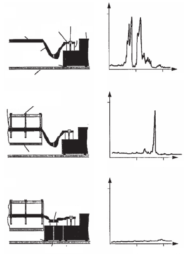
during temperature cycling require special attention. To reduce the
amplitude of vibrations introduced by the cryostat, it is important to
mechanically decouple the braid to a heavy mass (Bott et al., 1995) (see
Figure 17–2). Since only the sample is cooled, the scanner has to be
thermally isolated from the sample to avoid heat transfer to the sample.
One advantage of this approach for variable-temperature operation is
that the repeated recalibrations of the STM made necessary by tem-
perature-dependent changes in the piezo coeffi cients are avoided. But
large thermal gradients can create image drift problems and possible
disturbances due to heat transfer from the “hot” tip scanning the cold
sample (Xu et al., 1994).
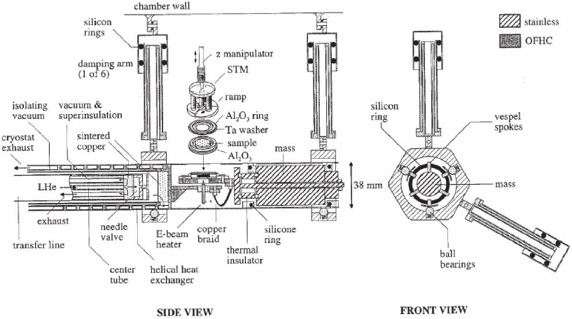
An example of a variable-temperature STM with fl ow cryostat cooling
the sample only is shown in Figure 17–3 (Behler et al., 1997). Other
examples are given in Bott et al. (1995), Horch et al. (1994), and Petersen
et al. (2001).
LHe fl ow cryostats can also be used to cool the entire STM. This
results in improved thermal stability due to thermal equilibrium
between all STM parts. If fast cooldown times are required, the STM
can be connected rigidly to the cold end of the fl ow cryostat (Mugele
et al., 1998; Zhang et al., 2001). This mandates a high mechanical stabil-
ity (high resonance frequency) of the STM so that the vibration fre-
quencies caused by the He fl ow are well below the eigenfrequency of
the STM. The microscope is surrounded by one or two radiation shields.
Higher mechanical stability can be obtained if the STM is suspended
with springs inside a radiation shield to provide vibration isolation

Chapter 17 Low-Temperature Scanning Tunneling Microscopy 1075
kryostat
sample
holder
sample
block
copper
braid
viton
manipulator
fixing screws
teflon
rigid tube
catched braid
viton
second mass
A
B
a)
a’)
b) b’)
c) c’)
1
1
2 kHz
1
1
2 kHz
1
1
2
kHz
arb.units
arb.units
arb.units
Figure 17–2. Mechanical decoupling of a copper braid connecting a fl ow
cryostat and a sample holder. Shown are modifi cations and their effect on the
noise spectrum. (a) Initial arrangement of the sample holder connected to the
cryostat by a copper braid. (a′) Fourier spectrum of the tunneling current with
noise showing up as peaks. (b) Resonance frequencies of cryostat are increased
by defi ning nodes with a rigid tube mounted on the cryostat with three screws
separated by 120° at each node. (b′) Fourier spectrum after modifi cation; noise
frequencies are shifted to higher frequencies. (c) Noise from the copper braid
coupling is damped out by fi xing the copper braid thermally isolated to a
massive block. (c′) Noise is greatly reduced. (From Bott et al., 1995.)

1076 U. Weierstall
from the cryostat (Wolkow, 1995; Stipe et al., 1999b) (see Figures 17–4
and 17–5).
2.2 STM with LHe Bath Cryostat
A bath cryostat is usually used if the whole STM is being cooled. The
bath cryostat serves as a large thermal reservoir that is being cooled
down prior to the measurements. This approach has been successfully
applied on a number of 4 K microscopes (Eigler and Schweizer, 1990;
Gaisch et al., 1992; Stranick et al., 1994b; Rust et al., 1997; Meyer, 1996;
Becker et al., 1998; Ferris et al., 1998; Harrell and First, 1999; Stroscio,
2000). If all parts of the system are allowed to reach thermal equilib-
rium, thermal drift may be virtually eliminated. Bath cryostat low-
temperature STMs operating in a rotatable magnetic fi eld have also
been built (Wittneven et al., 1997); some of them are
3
He refrigerated
and operate at about 250 mK (Pan et al., 1999; Kugler et al., 2000; Matsui
et al., 2003). Sample turnaround times for the very-low-temperature
variants are quite long since it can take 36 h to reach thermal equilib-
rium (Pan et al., 1999). LT-STMs with bath cryostats are diffi cult to use
for variable temperature measurements, e.g., study of diffusion and
phase transitions, since they use a large cold reservoir to cool the STM
and the temperature cannot be changed easily. Temperature control by
altering the exchange gas pressure in combination with a PID-
controlled heater has been achieved (Rust et al., 2001). Another way
to achieve measurements at different temperatures is to simply remove
Figure 17–3. Example of a variable-temperature STM for operation in the temperature range of 20–
300 K. Only the sample is cooled. Continuous fl ow cryostat on the left; arrows show helium fl ow. The
sample is thermally connected to the cryostat by a copper braid and mechanically decoupled with a
heavy stainless steel mass supported by O-rings. (From Behler et al., 1997.)

Chapter 17 Low-Temperature Scanning Tunneling Microscopy 1077
Continuous Flow
L–He/N
2
Cryostat
Sample at
8 K to 350 K
Cold Tip
Electrical
Feedthroughs
Inner
Access Door
Mo Sample
Holder
Piezotubes (4)
Sapphire
Laser Window
Samariam-
Cobalt Magnets
Inner Shield
Inconel
Springs (3)
W Balls (3)
and Tip
Mo Base Plate
Hole for
Dosing
Clamping
Screw
Outer Shield
Scale
2.5 cm
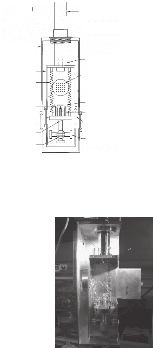
Figure 17–4. A variable-temperature scanning tunneling microscope cooled
with a continuous-fl ow cryostat. The STM and the sample are suspended from
three springs that provide the second stage of vibrational isolation. The design
allows for in situ dosing and irradiation of the sample as well as the exchange
of samples and tips. (From Stipe et al., 1999b.)
Figure 17–5. Low and variable
temperature STM in the author’s
laboratory, which is very similar
in design to the one by Stipe et
al. (1999b). Refer to Figure 17–4
for identifi cation of different
parts. The front of the outer radi-
ation shield and the sides of both
radiation shields are missing to
enable the inside to be viewed.
1078 U. Weierstall
liquid helium from the cryostat, giving rise to a temperature increase
of the microscope over days, thus enabling drift-free STM measure-
ments at well-defi ned temperatures up to 300 K. (Jeandupeux et al.,
1999)
Since the tunneling current has an exponential dependence on the
distance between tip and sample, vibrations can cause strong noise.
Therefore the construction of the STM scanner, consisting of tip holder,
sample holder, and actuators, should be as rigid as possible to increase
the mechanical eigenfrequency of the scanner. For typical tube scanner
setups this eigenfrequency lies in the range of 1–10 kHz. A two-stage
damping system consisting of an external damper (e.g., air damped
feet suspension of the whole UHV chamber) and an internal damper
(e.g., scanner suspended on springs and damped by eddy current
dampers) effectively isolates the tunneling gap from building vibra-
tions and acoustic noise. The two damping stages should have reso-
nance frequencies well below building and acoustic frequencies and
should be strongly damped (low Q-factor).
With a low-temperature STM the boiling cryogenic liquid produces
additional vibrations after the fi rst damping stage. Even worse, the
boiling liquid has to be in close proximity to the vibration-sensitive
scanner to enable good thermal contact to the scanner. Therefore there
are two contradictory demands for the design of a low-temperature
STM: mechanical decoupling of the STM head and thermal coupling
to the cryostat.
This problem has been solved by different groups in different ways
and in the following we will discuss three design examples. They all
have in common a helium bath cryostat surrounded by a liquid nitro-
gen cryostat, which acts as a radiation shield. They all have a two-stage
damping system; in the fi rst stage the whole UHV chamber is mechani-
cally decoupled from the fl oor by pneumatic dampers. The designs
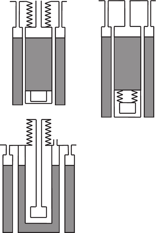
differ in the way the second damping stage is realized (see Figure
17–6):
The IBM-Rueschlikon/University Lausanne LT-STM designed by R.
Gaisch (Gaisch et al., 1992) uses a bellow to mechanically decouple the
liquid helium cryostat from the liquid nitrogen cryostat and the UHV
chamber. The STM, however, is rigidly connected to the liquid helium
cryostat, which results in very effective cooling. However, vibrations
from the cryostat can reach the STM unattenuated.
The LT-STM designed by G. Meyer and K.H. Rieder (Meyer, 1996)
has no damping between the liquid helium and the liquid nitrogen
cryostat; instead the STM is suspended from the He cryostat by small
extension springs and thereby is mechanically decoupled during mea-
surements. During cooldown the STM is lowered onto a copper plate
connected to the He cryostat to achieve good thermal contact. Since the
thin springs are not very good thermal conductors, the STM has to be
effectively shielded against incoming thermal radiation. This is
achieved by a two-stage radiation shield with the inner shield con-
nected to the He bath and the outer shield connected to the liquid
nitrogen bath. The STM is then almost thermally isolated during mea-
surements (see Figure 17–7).

Chapter 17 Low-Temperature Scanning Tunneling Microscopy 1079
AB
LN
2
LN
2
LN
2
LN
2
LHe
LHe
STM
STM
C
He
LN
2
LN
2
STM
LHe
Figure 17–6. Schematic comparison of different LT-STMs with bath cryostat.
(A) R. Gaisch/IBM Rueschlikon, (B) G. Meyer/FU Berlin, (C) D. Eigler/IBM
Almaden. The connection to the LHe cryostat and the second damping stage
of the STM is shown. (A) and (B) have a cryoshield surrounding the STM.
In (A) the LHe cryostat is decoupled from the LN
2
cryostat by bellows. In (B)
the STM is decoupled from the LHe cryostat by springs. In (C) the STM is
decoupled from the LHe cryostat by a bellows-supported pendulum. Thermal
contact is made by He exchange gas surrounding the evacuated pendulum.
