Czichos H., Saito T., Smith L.E. (Eds.) Handbook of Metrology and Testing
Подождите немного. Документ загружается.


178 Part B Chemical and Microstructural Analysis
technique directly determines the mass fraction of the
matrix species. In the second approach, the sum of the
mass fractions of all components of the sample is taken
as exactly unity (100%). Trace-level impurities in the
reagent are determined using one or more of the instru-
mental techniques described in this chapter. The sum
of the mass fractions of all detected impurities is sub-
tracted from 100% to yield the quoted purity (species
that are not detected are taken as present at a mass
fraction equal to half the detection limit for the given
species, with a relative uncertainty of ±100%; the cor-
responding value and uncertainty are included in the
calculation of the purity and its uncertainty). No assay
is performed per se.
In principle, both approaches yield the same re-
sult. However, difficulties arise in practice owing to the
shortcomings of each. In the classical assay, trace impu-
rities can contribute to the given assay, yielding a result
greater than the true value. For example, trace Br
−
is
typically titrated along with the matrix Cl
−
in classi-
cal titrimetric and coulometric assay procedures. Such
trace interferents contribute to the apparent assay to an
extent given by the actual mass fraction multiplied by
the ratio of the equivalent weight [4.84,90] of the matrix
species to that of the actual interferent, analogous to the
gravimetric factor in gravimetry. The equivalent weight
is given by the molar mass of the given species (calcu-
lated from IUPAC atomic weights [4.96]) divided by an
integer n. For coulometry, n is that given in (4.11). For
other methods, n is defined by the reaction that occurs
in the titration or precipitation process.
In the 100% minus impurities approach, the result
only includes those species that are actually sought. For
example, commercial high-purity reagents often state
a high purity, such as 99.999%, based on a semiquan-
titative survey of trace metal impurities. Other species,
notably occluded water in high-purity crystalline salts,
or dissolved gases in high-purity metals, are not sought,
but they may be present at high levels, such as 0.1%.
The purity with respect to the stated impurities is valid.
However, if the level of unaccounted-for impurities is
significant in comparison to the requirements for the
calibrant, the stated purity is not valid for use of the
reagent as a calibrant.
Figure 4.7 illustrates schematically the contrast-
ing advantages and disadvantages of both approaches
toward the purity of a hypothetical crystalline com-
pound. The total length of each bar corresponds to
the purity as obtained by the stated method(s). The
matrix compound is shown at the left in gray. Im-
purities (including water) are denoted by segments of
other shades at the right end of each bar. The up-
per bar shows the true composition as received. The
impurities are divided into two classes: those that con-
tribute to the classical assay, and those that do not. The
second bar shows the true composition after drying.
Each class of impurities is subdivided into a compo-
nent that is detected instrumentally and one that is
not. The two components that are detected instrumen-
tally are shown separately in the second line from the
bottom.
The third bar shows the classical assay without any
corrections for contributing impurities. The lower bar
represents the purity obtained from the 100% minus im-
purities approach. Each value has a positive bias with
respect to the true assay, the length of the matrix seg-
ment. The gravimetric factor represents the ratio of
equivalent weights noted above.
The fourth bar shows the result of the classical assay
corrected for instrumentally-determined impurities that
also contribute to the classical assay. This bar is closest
in length to the true assay, represented by the length of
the matrix segment. A small bias remains for impurities
that both evade instrumental detection and contribute to
the classical assay.
An additional problem with classical assays of ionic
compounds is that a single technique generally deter-
mines only a component of the matrix compound (such
as Cl
−
in the assay of KCl by titration with Ag
+
).
The reported mass fraction of the assay compound is
calculated assuming the theoretical stoichiometry. The
identity of the counterion (such as K
+
in an argentimet-
ric KCl assay) is assumed.
A more rigorous approach toward a true assay
of an ionic compound by classical techniques is to
perform independent determinations of the matrix com-
ponents. As an example, K
+
in KCl could be assayed by
gravimetry, with Cl
−
assayed by titrimetry or coulom-
etry. A rigorous version of each of these assays would
include corrections for contributing trace interferences
to the respective assays.
Several review articles [4.84–96] are available.
Part B 4.1

Analytical Chemistry 4.2 Microanalytical Chemical Characterization 179
4.2 Microanalytical Chemical Characterization
Establishing the spatial relationships of the chemical
constituents of materials requires special methods that
build on many of the bulk methods treated in the pre-
ceding portion of this chapter. There may be interest in
locating the placement of a trace chemical constituent
within an engineered structure, or in establishing the
extent of chemical alteration of a part taken out of ser-
vice, or in locating an impurity that is impacting on the
performance of a material. When the question of the rel-
ative spatial locations of different chemical constituents
is at the core of the measurement challenge, methods of
chemical characterization that preserve the structures of
interest during analysis are critical. Not all bulk analyt-
ical methods are suited for surface and/or microanalyt-
ical applications, but many are. In the remainder of this
chapter, some of the more broadly applicable methods
are touched upon, indicating their utility for establishing
chemical composition as a function of spatial location,
in addition to their use for quantitative analysis.
4.2.1 Analytical Electron Microscopy (AEM)
When a transmission electron microscope (TEM)is
equipped with a spectrometer for chemical analysis, it is
usually referred to as an analytical electron microscope.
The two most common chemical analysis techniques
employed by far are energy-dispersive x-ray spectrom-
etry (XEDS) and electron energy-loss spectroscopy
(EELS). In modern TEMs a field emission electron
source is used to generate a nearly monochromatic
beam of electrons. The electrons are then accelerated
to a user-defined energy, typically in the range of
100–400 keV, and focused onto the sample using a se-
ries of magnetic lenses that play an analogous role to
the condenser lens in a compound light microscope. Af-
ter interacting with the sample, the transmitted electrons
are formed into a real image using a magnetic objec-
tive lens. This real image is then further magnified by
a series of magnetic intermediate and projector lenses
and recorded using a charged coupled device (CCD)
camera.
Principles of the Technique. Images with a spatial res-
olution near 0.2 nm are routinely produced using this
technique. In an alternative mode of operation, the con-
denser lenses can be used to focus the electron beam
into a very small spot (less than 1 nm in diameter)
that is rastered over the sample using electrostatic de-
flection coils. By recording the transmitted intensity at
each pixel in the raster, a scanning transmission elec-
tron microscope (STEM) image can be produced. After
a STEM image has been recorded, it can be used to lo-
cate features of interest on the sample and the scan coils
can then be used to reposition the electron beam with
high precision onto each feature for chemical analy-
sis. As the beam electrons are transmitted through the
sample, some of them are scattered inelastically and
produce atomic excitations. Using an EELS spectrom-
eter, a spectrum of the number of inelastic scatters as
a function of energy loss can be produced. Simultane-
ously, an XEDS spectrometer can be used to measure
the energy spectrum of x-rays emitted from the sam-
ple as the atoms de-excite. Both of these spectroscopies
can provide detailed quantitative information about the
chemical structure of the sample with very high spatial
resolution.
In many ways EELS and XEDS are complemen-
tary techniques, and the limitations of one spectroscopy
are often offset by the strengths of the other. Because
elements with low atomic number do not fluoresce effi-
ciently, XEDS begins to have difficulty with elements
lighter than sodium and is difficult or impossible to
use for elements below carbon. In contrast, EELS is
very efficient at detecting light elements. Because EELS
has much better energy resolution than XEDS (≈ 1eV
for EELS and 130 eV for XEDS), it is also capable
of extracting limited information about the bonding
and valence state of the atoms in the analysis region.
The two main drawbacks to EELS are that the sam-
ples need to be very thin compared to XEDS samples,
and that it places greater demands on the analyst, both
experimentally during spectrum acquisition and theo-
retically during interpretation of the results. Because
XEDS works well on relatively thick samples and is eas-
ier to execute, it enjoys widespread use, while EELS is
often considered a more specialized technique.
Nature of the Sample. Perhaps the single most im-
portant drawback to AEM is that all samples must be
thinned to electron transparency. The maximum accept-
able thickness varies with the composition of the sample
and the nature of the analysis sought, but in most cases
the samples must be less than ≈ 500 nm thick. For
quantitative EELS, the samples must be much thinner:
a few tens of nanometers thick at most. Another impor-
tant limitation is that the samples be compatible with
the high vacuum environment required by the electron
optics. Fortunately, a wide array of sample prepara-
Part B 4.2
180 Part B Chemical and Microstructural Analysis
Counts
30 000
20 000
10 000
0
02 4 6 8
Energy (keV)
Integrated EDX
C
O
Si
Fe
Fe
Cu
Mg
Al
K
Ca
Fe
Fe
Cu
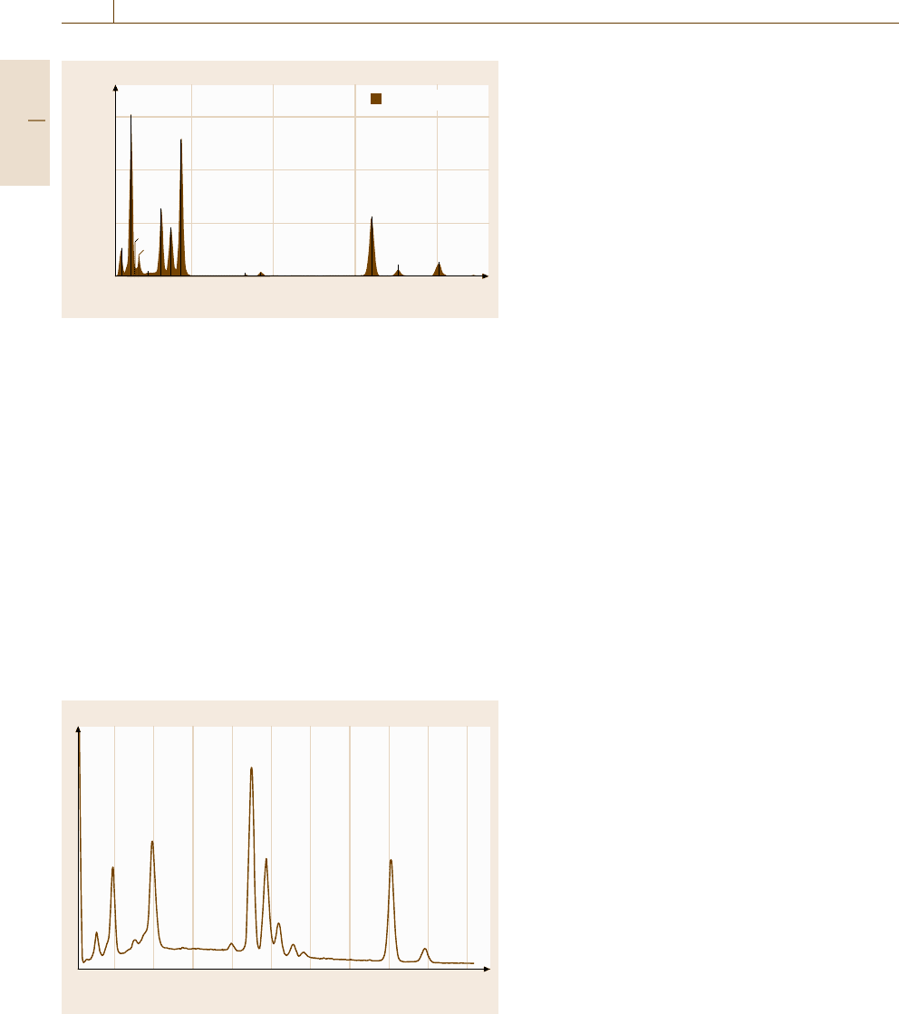
Fig. 4.8 Analytical electron microscopy: example XEDS spectrum
from a sample containing C, O, Mg, Al, Si, K, Ca and Fe. The Cu
peaks are from the sample mount
tion techniques have been developed over the years to
convert macroscopic pieces of (sometimes wet) mater-
ial into very thin slices suitable for AEM: dimpling,
acid jet polishing, bulk ion milling, mechanical polish-
ing, focused ion beam (FIB) processing, and diamond
knife sectioning using an ultramicrotome. Preparation
of high-quality AEM samples that are representative of
the parent material without introducing serious artifacts
remains one of the most important tasks facing the AEM
analyst.
Qualitative Analysis. The AEM is a powerful tool for
the qualitative chemical analysis of nanoscale samples.
Intensity
012345678910
Energy
O K
α
Cu L
α1
Y L
α1
BaL
α1
CuK
α
Y L
γ1
Y L
1
Al K
α
Y L
β1
BaL
β2
BaL
γ1
BaL
γ3
BaL
β1
CuK
β1
BaL
1
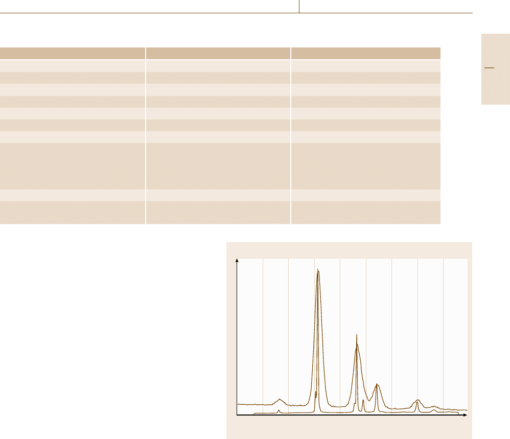
Fig. 4.9 Energy-dispersive spectrometry (EDS)ofanYBa
2
Cu
3
O
7−x
single crystal with a trace aluminum constituent. Beam energy
=20 keV
The XEDS spectrometer can be used to detect most
elements present in the sample at concentrations of
1mg/g(0.1% mass fraction) or higher (see Fig. 4.8).
EELS can be used in many cases down to a detec-
tion limit of 100 μg/g, depending on the combination
of elements present. While these numbers are not im-
pressive in terms of minimum mass fraction (MMF)
sensitivity, it should be noted that this performance is
available with spatial resolutions measured in nanome-
ters and for total sample masses measured in attograms.
In favorable cases, single-atom sensitivity has been
demonstrated in the AEM for several elements, thus es-
tablishing it as a leader in minimum detectable mass
(MDM) sensitivity.
Traceable Quantitative Analysis. Through the use of
standards and the measurement of empirical detec-
tor sensitivity factors (Cliff–Lorimer k-factors), XEDS
measurements in the AEM can be made quantitative.
The precision of the measurement is often limited by
the total signal available (related to the sample thick-
ness and elemental abundances), while the accuracy is
affected by poorly-known sample geometry and absorp-
tion effects. Traceability of the results is limited by the
extreme rarity of certified reference materials with suffi-
cient spatial homogeneity suitable for the measurement
of k-factors. EELS measurements can be quantified by
a first-principles approach that does not require stan-
dards, but this method is limited in practice by our
inability to compute accurate scattering cross-sections
and our incomplete understanding of solid-state beam–
sample interactions.
Several review articles [4.97–100] are available.
4.2.2 Electron Probe X-ray Microanalysis
Most solid matter is characterized on the microscopic
scale by a chemically differentiated microstructure with
feature dimensions in the micrometer to nanometer
range. Many physical, biological and technological
processes are controlled on a macroscopic scale by
chemical processes that occur on the microscopic
scale. The electron probe x-ray microanalyzer (EPMA)
is an analytical tool based upon the scanning elec-
tron microscope (SEM) that uses a finely focused
electron beam to excite the specimen to emit char-
acteristic x-rays. The analyzed region has lateral and
depth dimensions ranging from 50 nm to 5 μm, de-
pending upon specimen composition, the initial beam
energy, the x-ray photon energy, and the exact analytical
conditions.
Part B 4.2
Analytical Chemistry 4.2 Microanalytical Chemical Characterization 181
Table 4.3 Comparison of the characteristics of EDS and WDS x-ray spectrometers
Feature EDS (semiconductor) WDS
Energy range 0.1–25 keV (Si) 0.1–12 keV (4 crystals)
0.1–100 keV (Ge)
Resolution at MnK
α
130 eV (Si); 125 eV (Ge) 2–20 eV (E, crystal)
Instantaneous energy coverage Full range Resolution, 2–20 eV
Deadtime 50 MS 1 MS
Solid angle (steradian) 0.05–0.2 0.01
Quantum efficiency ≈100%, 3–15 keV (Si) < 30%, variable
Maximum count rate, EDS ≈ 3 kHz (best resolution) 100 kHz (single photon energy)
Maximum count rate, SDD ≈ 30 kHz (mapping)
≈ 15 kHz (best resolution)
≈400 kHz (mapping)
Full spectrum collection 10–200 s 600–1800 s
Special strengths Views complete spectrum for qualitative Resolves peak interferences; rapid pulses
analysis at all locations for composition mapping
Principles of the Technique. The EPMA/SEM is ca-
pable of quantitatively analyzing major, minor and
trace elemental constituents, with the exceptions of H,
He and Li, at concentrations as low as a mass frac-
tion of ≈ 10
−5
. The technique is generally considered
nondestructive and is typically applied to flat, metallo-
graphically polished specimens. The SEM permits ap-
plication of the technique to special cases such as rough
surfaces, particles, thin layers on substrates, and un-
supported thin layers. Additionally, the SEM provides
a full range of morphological imaging and structural
crystallography capabilities that enable characteriza-
tion of topography, surface layers, lateral compositional
variations, crystal orientation, and magnetic and elec-
trical fields over the micrometer to nanometer spatial
scales. Two different types of x-ray spectrometers are
in widespread use, the energy-dispersive spectrometer
(EDS) and the wavelength-dispersive (or crystal diffrac-
tion) spectrometer (WDS). The characteristics of these
spectrometers are such that they are highly complemen-
tary: the weaknesses of one are substantially offset by
the strengths of the other. Thus, they are often em-
ployed together on the same electron beam instrument.
The recent emergence of the silicon drift detector (SDD)
has extended the EDS output count rate into the range
100–500 kHz. Figure 4.9 shows a typical EDS spec-
trum from a multicomponent specimen, YBa
2
Cu
3
O
7
,
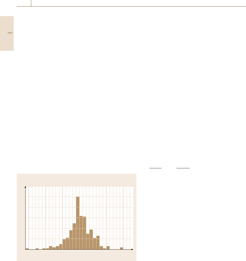
demonstrating the wide energy coverage. Figure 4.10
shows a comparison of the EDS and WDS spectra for
a portion of the dysprosium L-series. The consider-
able improvement in the spectral resolution of WDS
compared to EDS is readily apparent. Table 4.3 com-
Intensity
Energy
4.93 5.93 6.93 7.93 4.925.43 6.43 7.43 8.42
DyL
α1
DyL
β1
DyL
β3
DyL
β2
DyL
β5
DyL
γ5
DyL
γ1
DyL
γ3
DyL
β10
DyL
β4
DyL
α2
DyL
α2
DyL
0
DyL
η
Fig. 4.10 Comparison of EDS and WDS for dysprosium L-family
x-rays excited with a beam energy of 20 keV
pares a number of the spectral parameters of EDS and
WDS.
Qualitative Analysis. Qualitative analysis, the identifi-
cation of the elements responsible for the characteristic
peaks in the spectrum, is generally straightforward for
major constituents (for example, those present at con-
centrations > 0.1% mass fraction), but can be quite
challenging for minor (0.01–0.1% mass fraction) and
trace constituents (< 0.01% mass fraction). This is es-
pecially true for EDS spectrometry when peaks of
Part B 4.2
182 Part B Chemical and Microstructural Analysis
minor and trace constituent peaks are in the vicin-
ity (< 100 eV away) of peaks from major constituents.
Such interferences require peak deconvolution, espe-
cially when the minor or trace element is a light element
(Z < 18), for which only one peak may be resolvable by
EDS. Automatic computer-aided EDS qualitative anal-
yses must always be examined manually for accuracy.
The superior spectral resolution of the WDS can gen-
erally separate major/minor or major/trace peaks under
these conditions, and is also not susceptible to the spec-
tral artifacts of the EDS, such as pile-up peaks and
escape peaks. However, additional care must be taken
with WDS to avoid incorrectly interpreting higher or-
der reflections (n = 2, 3, 4,... in the Bragg diffraction
equation) as peaks arising from other elements.
Quantitative Analysis: Spectral Deconvolution. Quan-
titative analysis proceeds in three stages:
1. extraction of peak intensities;
2. standardization; and
3. calculation of matrix effects.
For EDS spectrometry, the background is first
removed by applying a background model or a mathe-
matical filter. Peak deconvolution is then performed by
the method of multiple linear least squares (MLLSQ).
MLLSQ requires a model of the peak shape for each el-
ement determined on the user’s instrument, free from
NBS (1975) Heinrich–Yakowitz Binary Data ZAF
Frequency
60
50
40
30
20
10
0
–15 –10 –5 0 5 10
Relative error (%)
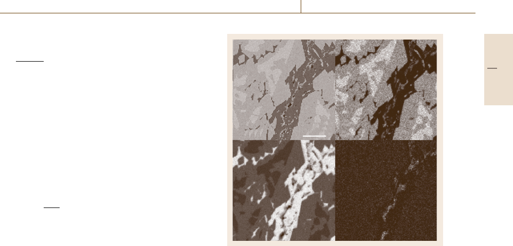
Fig. 4.11 Distribution of analytical relative errors (defined as
(100% × [measured −true]/true)) for binary alloys as measured
against pure element standards. Matrix correction by National Bu-
reau of Standards ZAF; wavelength-dispersive x-ray spectrometry;
measurement precision typically 0.3% relative standard deviation
(after Heinrich and Yakowitz)
interferences from other constituents. A peak region
from an unknown that consists of contributions from
two or more constituents is deconvolved by construct-
ing linear combinations of the reference peak shapes
for all constituents. The synthesized peaks are com-
pared with the measured spectrum until the best match
is obtained, based upon a statistical criterion such as
minimization of chi-squared, determined on a channel-
by-channel basis. For WDS spectrometry, the resolution
is normally adequate to separate the peak interferences
so that the only issue is the removal of background. Be-
cause the background changes linearly over the narrow
energy window of a WDS peak, an accurate background
correction can be made by interpolating between two
background measurements on either side of the peak.
Quantitative Analysis: Standardization. The basis for
accurate quantitative electron probe x-ray microanaly-
sis is the measurement of the ratio of the intensity of
the x-ray peak in the unknown to the intensity of that
same peak in a standard, with all measurements made
for the same beam energy, known electron dose (beam
current × time), and spectrometer efficiency. This ra-
tio, known as the k-value, is proportional to the ratio
of mass concentrations for the element in the specimen
and standard
I
A,spec
I
A,std
=k ≈
C
A,spec
C
A,std
. (4.12)
This standardization step quantitatively eliminates the
influence of detector efficiency, and reduces the impact
of many physical parameters needed for matrix cor-
rections. A great strength of EPMA is the simplicity
of the required standard suite. Pure elements and sim-
ple stoichiometric compounds for those elements that
are unstable in a vacuum under electron bombardment
(such as pyrite, FeS
2
for sulfur) are sufficient. This is
a great advantage, since making multielement mixtures
that are homogeneous on the micrometer scale is gener-
ally difficult due to phase separation.
Quantitative Analysis: Matrix Correction. The relation-
ship between k and C
A,spec
/C
A,std
is not an equality
because of the action of matrix or interelement effects.
That is, the presence of element B modifies the intensity
of element A as it is generated, propagated and detected.
Fortunately, the physical origin of these matrix effects is
well-understood, and by a combination of basic physics
as well as empirical measurements, multiplicative cor-
rection factors for atomic number effects Z, absorption
Part B 4.2
Analytical Chemistry 4.2 Microanalytical Chemical Characterization 183
A and fluorescence F have been developed
C
A,spec
C
A,std
=kZA F . (4.13)
From the previous discussion, it is obvious that all three
matrix effects – Z, A,andF – depend strongly on the
composition of the measured specimen, which is the
unknown for which we wish to solve. The calculation
of matrix effects must therefore proceed in an iterative
fashion from an initial estimate of the concentrations
to the final calculated value. The measured k-values
are used to provide the initial estimate of the speci-
men composition by setting the concentrations equal to
normalized k-values
C
i,1
=
k
i
Σk
i
, (4.14)
where i denotes each measured element. The initial con-
centration values are then used to calculate an initial set
of matrix corrections, which in turn are used to cal-
culate predicted k-values. The predicted k-values are
compared with the experimental set, and if the values
agree within a defined error, the calculation is termi-
nated. Otherwise, the cycle is repeated. Convergence is
generally found within three iterations.
This matrix correction procedure has been tested
repeatedly over the last 25 years by using various mi-
crohomogeneous materials of known composition as
test unknowns, including alloys, minerals, stoichiomet-
ric binary compounds, and so on. A typical distribution
of relative errors (defined as [measured−true]/true ×
100%) for binary alloys analyzed against pure element
standards is shown in Fig. 4.11.
Compositional Mapping. A powerful method of pre-
senting x-ray microanalysis information is in the form
of compositional maps or images that depict the area
distribution of the elemental constituents. These maps
can be recorded simultaneously with SEM images that
provide morphological information [4.101–103]. The
digital output from a WDS, EDS or SDD over a de-
fined range of x-ray photon energy corresponding to the
peaks of interest is recorded at each picture element
(pixel) scanned by the beam. The most sophisticated
level of compositional mapping involves collecting
a spectrum, or at least a number of spectral intensity
windows for each picture element of the scanned image.
These spectral data are then processed with the back-
ground correction, peak deconvolution, standardization,
and matrix correction necessary to achieve quantitative
analysis. The resulting maps are actually records of the
Ni
100 µm
Al
Fe
BSE
Fig. 4.12 Compositional maps (Ni, Al and Fe) and an SEM
image (backscattered electrons, BSE) of Raney nickel
(Ni-Al) alloy, showing a complex microstructure with a mi-
nor iron constituent segregated in a discontinuous phase
local concentrations, so that when displayed, the gray or
color scale is actually related to the concentration. Fig-
ure 4.12 shows examples of compositional maps for an
aluminum-nickel alloy.
Several review articles [4.104–106] are available.
4.2.3 Scanning Auger Electron Microscopy
Scanning Auger electron microscopy is an electron
beam analytical technique based upon the scanning
electron microscope. Auger electrons are excited in
the specimen by a finely focused electron beam with
a lateral spatial resolution of ≈2 nm point-to-point in
current state-of-the-art instruments. An electron spec-
trometer capable of measuring the energies of emitted
Auger electrons in the range of 1–3000 eV is employed
for qualitative and quantitative chemical analysis. As
in electron-excited x-ray spectrometry, the positions of
the peaks are representative of the chemical composi-
tion of the specimen. The inelastic mean free path for
Auger electrons is on the order of 0.1–3 nm, which
means that only the Auger electrons that are pro-
duced within a few nanometers of the specimen surface
are responsible for the analytical signal. The current
state-of-the-art instruments are capable of providing
true surface characterization at ≈ 10 nm lateral resolu-
tion.
Part B 4.2

184 Part B Chemical and Microstructural Analysis
Fig. 4.13 SE image of particle, 25 μmfieldofview
Principles of the Technique. A primary electron beam
interacting with a specimen knocks out a core electron,
creating a core level vacancy. As a higher energy level
electron moves down to fill the core level vacancy, en-
ergy is released in the form of an Auger electron, with
the energy corresponding to the difference between the
two levels. This is the basis for Auger electron spec-
troscopy (AES). The core-level vacancy can also be
created by an x-ray photon, and this is the basis for x-
ray photoelectron spectroscopy. The energy difference
between the higher energy electron and the core level
can also be released as a characteristic x-ray photon,
and this is the basis for electron probe microanalysis.
Intensity
300 000
250 000
200 000
150 000
100 000
50 000
0
500 1000 1500 2000 2500
Energy (eV)
C
O
Cu
Fig. 4.14 Direct AES of copper with
carbon and oxygen
The primary electron beam in an Auger microscope
operates between 0.1 and 30 kV, and beam currents
are on the order of nanoamps for analysis. Tungsten
and lanthanum hexaboride electron guns can be used
for AES, but field emission electron guns are the best
choice because of the higher current density. It is desir-
able for AES to have more electrons in a small spot, and
field emission guns deliver the smallest spot sizes nor-
malized to beam current. Auger microscopes are also
very good scanning electron microscopes, capable of
producing secondary electron images (see Fig. 4.13)of
the specimen as well as backscattered electron images
if so equipped.
Auger electrons are produced throughout a sam-
ple volume defined by the interaction of the primary
electron beam and the specimen. Auger electrons are
relatively low in energy and so can only travel a small
distance in a solid. Only the Auger electrons that are
created close to the surface, within a few nanometers,
have sufficient mean free path to escape the specimen
and be collected for analysis. Since the Auger informa-
tion only comes from the first few nanometers of the
specimen surface, AES is considered a surface-sensitive
technique. Several review articles are available.
Nature of the Sample. The surface sensitivity of AES
requires the specimen to have a clean surface free of
contamination. For this reason, Auger microscopes are
ultrahigh vacuum (UHV) in the specimen chamber,
which is on the order of 10
−8
Pa. Steps must be taken
to clean specimens prior to introduction into the Auger
microscope so that they are free of volatile organic com-
pounds that can contaminate the chamber vacuum. The
Auger specimen chamber is equipped with an argon ion
gun for sputter cleaning-off the contamination or ox-
Part B 4.2
Analytical Chemistry 4.2 Microanalytical Chemical Characterization 185
Intensity
Energy (eV)
2500
0
–2500
–5000
–7500
–10 000
500 1000 1500 2000 2500
Fig. 4.15 Derivative AES of copper
with carbon and oxygen
ide layer that coats specimens as a result of transporting
them in air.
Investigation of a buried structure or an interface
that is deeper than the Auger escape depth can be ac-
complished by Auger depth profiling. In Auger depth
profiling, the instrument alternates between Ar ion sput-
tering of the surface and Auger analysis of the surface
until, as material is sputtered away, the elemental com-
position changes with depth.
Qualitative/Quantitative Analysis. Auger electrons are
recorded as a function of their energy by the electron
spectrometer in the Auger microscope and provide ele-
mental as well as bonding information. There are two
10 µm
Fig. 4.16 ESEM image of hydrated, freshwater algal sur-
face
types of electron spectrometer, the cylindrical mirror
analyzer (CMA) and the hemispherical analyzer (HSA).
The CMA is concentric with the electron beam and has
a greater throughput because of its favorable solid an-
gle. The HSA has the higher energy resolution, which
is desirable for unraveling overlapped peaks. In the
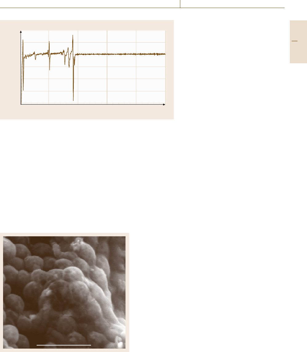
direct display mode (Fig. 4.14), peaks on the sloping
background of an Auger spectrum indicate the pres-
ence of elements between Li and U. Spectra can also
be displayed in the derivative mode (Fig. 4.15), which
removes the sloping background and random noise.
Auger quantitation is complicated by many instrumen-
tal factors and is normally done with sensitivity factors
normalized to an elemental silver Auger signal collected
under the same instrumental conditions.
Several review articles [4.107–109] are available.
4.2.4 Environmental Scanning Electron
Microscope
The environmental scanning electron microscope
(ESEM) is a unique modification of the conventional
scanning electron microscope (SEM). While the SEM
operates with a modest vacuum (≈10
−3
Pa), the ESEM
is able to operate with gas pressures ranging be-
tween 10 and 2700 Pa in the specimen chamber due
to a multistage differential pumping system separated
by apertures. The relaxed vacuum environment of the
ESEM chamber allows examination of wet, oily and
dirty specimens that cannot be accommodated in the
higher vacuum of a conventional SEM specimen cham-
ber. Perhaps more significant, however, is the ability
of the ESEM to maintain liquid water in the specimen
chamber with the use of a cooling stage (Fig. 4.16). The
capability to provide both morphological and compo-
Part B 4.2
186 Part B Chemical and Microstructural Analysis
C
O
Na
Mg
Al
Si
P
S
Cl
In
Fe
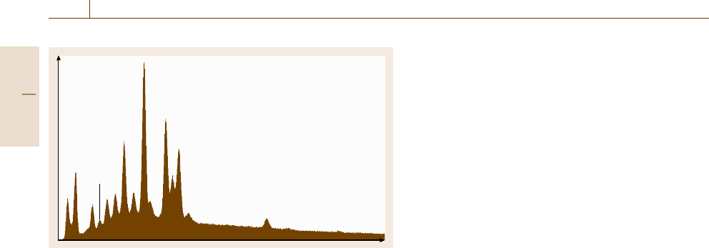
Fig. 4.17 EDS image of biological solids from a wastewater treat-
ment facility. The indium peak is caused by the support stub
sitional analysis of hydrated samples has allowed the
ESEM to benefit a number of experimental fields, rang-
ing from material science to biology. Several review
articles are available.
Principles of the Technique. The ESEM utilizes
a gaseous secondary electron detector (GSED)that
takes advantage of the gas molecules in the speci-
men chamber. The primary electron beam, operating
between 10 and 30 kV, are generated from tungsten,
lanthanum hexaboride, or field emission electron guns.
When a primary electron beam strikes a specimen, it
generates both backscattered and secondary electrons.
Backscattered electrons are energetic and are collected
by a line-of-sight detector. The secondary electrons are
low-energy and, as they emerge from the specimen,
are accelerated towards the GSED by the electric field
set up between the positive bias on the GSED and the
grounded specimen stage. These secondary electrons
collide with gas molecules, resulting in ionizations and
more secondary electrons, which are subsequently ac-
celerated in the field. This amplification process repeats
itself multiple times, generating imaging gain in the gas.
A byproduct of this process is that the gas molecules are
left positively charged and act to discharge the excess
electrons that accumulate on an insulating specimen
from the primary electron beam. This charge neutral-
ization obviates the need for conductive coatings or
low-voltage primary beams, as are often used in con-
ventional SEM to prevent surface charging under the
electron beam.
Secondary and backscattered electrons are produced
throughout the interaction volume of the specimen, the
depth of which is dependent on the energy of the pri-
mary electron beam and the specimen composition. The
backscattered electrons contain most of the energy of
the primary electron beam and can therefore escape
from a greater depth in the specimen. In contrast, sec-
ondary electrons are only able to escape from the top
10 nm of the specimen, although backscattered elec-
trons can also create secondary electrons prior to exiting
the sample and provide sample depth information to the
image. In general, it is possible to routinely resolve fea-
tures ranging from 10 to 50 nm. However, the primary
electron beam can also interact with the gas molecules,
resulting in beam electrons being scattered out of the
focused electron beam into a wide, diffuse skirt that
surrounds the primary beam impact point. Similarly,
chamber gas composition can also impact the amplifi-
cation process and thereby affect image quality.
Qualitative/Quantitative Analysis. In addition to the
image-producing backscattered and secondary electrons
that are generated when a primary beam strikes a speci-
men, there are also electron beam interactions that result
in the generation of x-rays from the interaction volume.
The energy of the resulting x-rays is representative of
the chemical composition within the interaction volume
and can be measured with an EDS. X-ray counts are
plotted as a function of their energy, and the result-
ing peaks can be identified by element and line with
standard x-ray energy tables (Fig. 4.17). EDS in the
ESEM is considered a qualitative method of composi-
tional analysis since x-rays may originate hundreds of
micrometers from the impact point of the primary elec-
tron beam as a result of electrons scattered out of the
beam by gas molecules.
Several review articles [4.110–117] are available.
4.2.5 Infrared and Raman Microanalysis
Infrared and Raman microanalysis is the application of
Raman and/or infrared (IR) spectroscopies to the anal-
ysis of microscopic samples or sample areas. These
techniques are powerful approaches to the characteri-
zation of spatial variations in chemical composition for
complex, heterogeneous materials, operating on length
scales similar to those accessible to conventional opti-
cal microscopy while also yielding the high degree of
chemical selectivity that underlies the utility of these
vibrational spectroscopies on the macroscale. Sample
analyses of this type are particularly useful in estab-
lishing correlations between macroscopic performance
properties (such as mechanical and chemical stabil-
ity, biocompatibility) and material microstructure, and
are thus a useful ingredient in the rational design of
Part B 4.2
Analytical Chemistry 4.2 Microanalytical Chemical Characterization 187
high-performance materials. Several review articles are
available.
Principles of the Technique. A typical Raman micro-
scope comprises a laser excitation source, a light micro-
scope operating in reflection mode, and a spectrometer.
Photons inelastically scatter from the sample at frequen-
cies shifted from that of the excitation radiation by the
energies of the fundamental vibrational modes of the
material, giving rise to the chemical specificity of Ra-
man scattering. A high-quality microscope objective is
used both to focus the excitation beam to an area of
interest on the sample and to collect the backscattered
photons. In general, the Rayleigh (elastic) scattering
of the incident photons is many orders of magnitude
more efficient than Raman scattering. Consequently, the
selective attenuation of the Rayleigh photons is a crit-
ical element in the detection scheme; recent advances
in dielectric filter technology have simplified this prob-
lem considerably. The attainable spatial resolution is,
in principle, limited only by diffraction, allowing sub-
micrometer lateral resolution in favorable cases. Fine
vertical resolution can also be achieved through the
use of a confocal aperture, opening up the possibility
of constructing 3-D chemical images through the use
of Raman depth profiling. Raman images are usually
acquired by raster scanning the sample with synchro-
nized spectral acquisition. Wide-field illumination and
imaging configurations have been explored, but they
Absorbance
2.5
2
1.5
1
0.5
0
1000 1500 2000 2500 3000 3500 4000
Talc
Wavenumber (cm
–1
)
a) b)
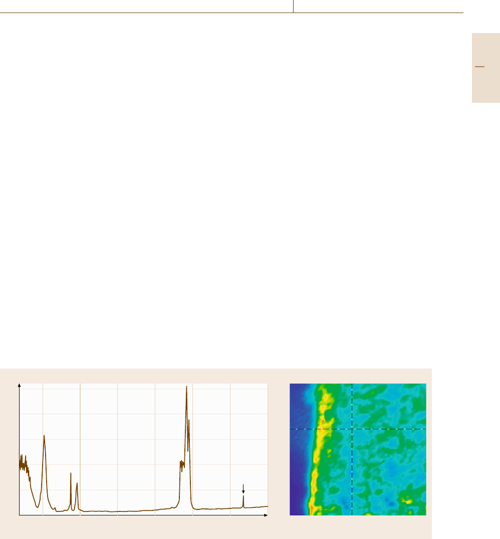
Fig. 4.18 (a) IR microspectrum of a thin film microtome section of injection-molded thermoplastic olefin. The sharp
spectral feature at 3700 cm
−1
is due to the OH stretching vibration of the talc filler (b) 325 μm×325 μm IR image of
a thermoplastic olefin cross-section wherein the amplitude of the talc band is plotted on a blue (low amplitude) to red
(high amplitude) color scale. The yellow-red band on the left side of the film is due to a talc-rich layer formed near the
mold surface
are generally only useful in limited circumstances due
to sensitivity issues. Chemical composition maps can
easily be extracted from Raman images by plotting the
intensities of bands due to particular material compo-
nents. Subtle spectral changes (such as band shifts) can
also be exploited to generate spatial maps of other ma-
terial properties, such as crystallinity and strain.
A typical IR microscope system consists of a re-
search-grade Fourier transform (FT) IR spectrometer
coupled to a microscope that operates in both reflec-
tion and transmission modes. Reflective microscope
objectives are widely used due to their uniformly
high reflectivity across the broad infrared spectral re-
gion of interest and their lack of chromatic aberration.
The spectrum of IR light measured upon transmission
through or reflection from the sample is normalized
to a suitable background spectrum. The normalized
spectrum displays attenuation of the IR light reach-
ing the detector due to direct absorption at frequencies
resonant with the active vibrational modes of the sam-
ple components. The frequencies at which absorption
occurs are characteristic of the presence of particu-
lar functional groups (such as C=O), resulting in the
powerful chemical specificity of the measured spec-
tra (Fig. 4.18). Microscopes employing a sample raster
scanning approach to image acquisition were the first
available, but have now been joined by those employing
a wide-field illumination, array-based imaging detec-
tion approach. The spatial resolution attainable with this
Part B 4.2
