Blum W., Riegler W., Rolandi L. Particle Detection with Drift Chambers
Подождите немного. Документ загружается.

6.1 Linear Signal Processing 187
i(t)
I(s)
w(t)
W(s)
o(t) = ∫w(t-t')i(t')dt'
O(s) = W(s) I(s)
Fig. 6.3 A linear device is characterized by the transfer function W (s) in the Laplace domain or
the delta response w(t)=L
−1
[W (s)] in the time domain
The step function
Θ
(t) is defined in Eq. (6.16). For k = 0wehaveL
−1
[1]=
δ
(t).
If a
i
> 0, the delta response tends to infinity for t → ∞, so the criterion for stability
of a linear system is given by the requirement that the real parts of all poles of W(s)
must be negative. In the case where a
i
+ ib
i
is a root of a polynomial, the complex
conjugate a
i
−ib
i
is also a root of the polynomial. Thus the terms in Eq. (6.13)
always appear in complex conjugate pairs, the imaginary part is cancelled, and the
delta response is always real.
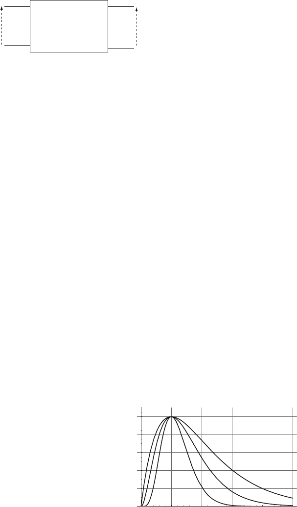
Figure 6.4 shows an example of the terms from Eq. (6.13) for k = 2,4,6 and b
i
=
0. In this book we mainly discuss transfer functions with real poles. The imaginary
parts of poles arise from inductances. (As these cannot be implemented physically as
coils in integrated devices, one would make them feedback loops using operational
amplifiers).
6.1.3 CR, RC, Pole-zero and Zero-pole Filters
In this section we discuss four elementary filters that illustrate the formalism out-
lined in the previous section. They are also elementary in the sense that by cascading
these four filter types we can construct any desired transfer function W(s) with real
poles. If we wanted to construct the most general transfer function W(s) also in-
cluding complex poles we would have to add a few elementary circuits containing
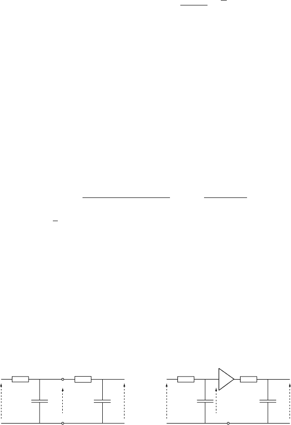
an inductance L. The CR and RC filters are shown in Fig. 6.5. The output voltages
of the two filters for an input voltage signal V (s)=L [v(t)] are
Fig. 6.4 The delta response
w(t) of a linear network with
real poles consists of the sum
of shapes indicated in this
figure. In the case where
W(s) has complex poles we
find terms with an oscillatory
behaviour of frequency b
i
/2
π
and a damping factor of
exp(−a
i
t)
1 2 3 4 5
0.2
0.4
0.6
0.8
1
k = 6
t/t
p
k = 4
k = 2
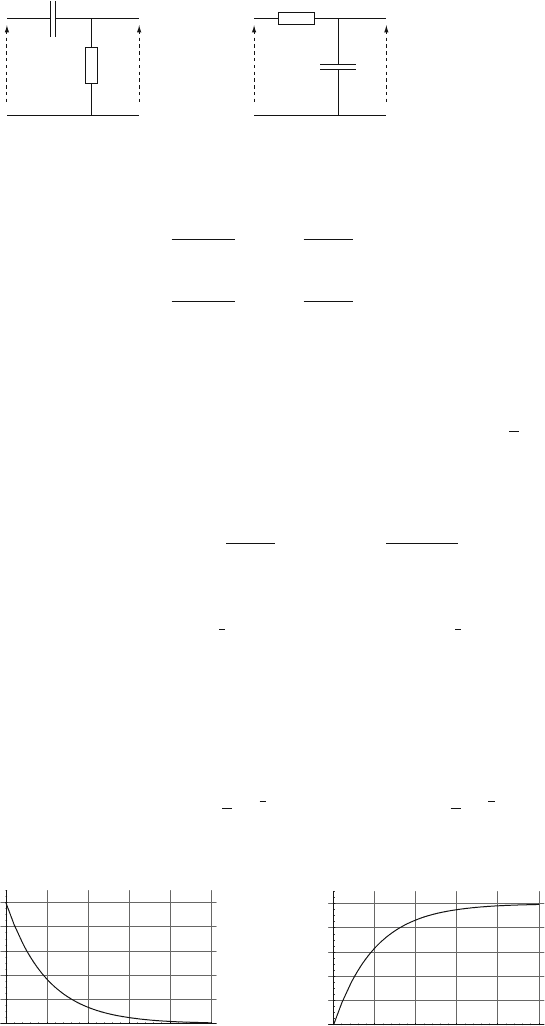
188 6 Electronics for Drift Chambers
R
R
C
C
v(t)
v(t)
v
1
(t) v
2
(t)
Fig. 6.5 A CR (left) and RC (right) filter consisting of a resistor R and a capacitor C. A voltage
signal v(t) is transformed into the output voltage signals v
1
(t) and v
2
(t)
V
1
(s)=
sRC
1+ sRC
V(s)=
s
τ
1+ s
τ
V(s)=W
CR
(s)V(s) (6.14)
V
2
(s)=
1
1+ sRC
V(s)=
1
1+ s
τ
V(s)=W
RC
(s)V(s). (6.15)
The value
τ
= RC is the characteristic time constant of the filters. In the following
we frequently use the step function
Θ
(t), which is defined by
v(t)=
Θ
(t)=
$
0 t ≤0
1 t > 0
V(s)=L [v(t)] =
1
s
. (6.16)
Applying this voltage step of amplitude V
0
at the inputs of the two filters yields the
output signals
V
1
(s)=
V
0
τ
1+ s
τ
V
2
(s)=
V
0
s(1+ s
τ
)
. (6.17)
Returning to the time domain, we find
v
1
(t)=V
0
e
−
t
τ
Θ
(t) v
2
(t)=V
0
(1−e
−
t
τ
)
Θ
(t) (6.18)
The two responses are shown in Fig. 6.6. The output of the CR filter decays exponen-
tially from the value V
0
to 0, while the output of the RC filter increases exponentially
from 0 to V
0
. We can also calculate the output signal in the time domain by finding
the delta response of the circuit w(t)=L
−1
[W(s)] and convoluting it with the input
signal:
w
CR
(t)=
δ
(t)+
1
τ
e
−
t
τ
Θ
(t) w
RC
(t)=
1
τ
e
−
t
τ
Θ
(t) (6.19)
1 2 3 4 5
0.2
0.4
0.6
0.8
1
1 2 3 4 5
0.2
0.4
0.6
0.8
1
v
1
/
V
0
v
2
/
V
0
t
/τ t
/τ
Fig. 6.6 Output of the CR and RC filter for a voltage step function input
6.1 Linear Signal Processing 189
v
1
(t)=
t
0
δ
(t −t
) −
1
τ
e
−
t−t
τ
Θ
(t −t
)
V
0
Θ
(t
)dt
= V
0
e
−
t
τ
Θ
(t)
v
2
(t)=
t
0
1
τ
e
−
t−t
τ
Θ
(t −t
)
V
0
Θ
(t
)dt
= V
0
(1−e
−
t
τ
)
Θ
(t) . (6.20)
We find the same result as before. If we replace s by i
ω
we have the transfer function
in the Fourier (frequency) domain:
W
CR
(i
ω
)=
i
ωτ
1+ i
ωτ
=
ωτ
√
1+
ω
2
τ
2
exp [i arctan1/
ωτ
],
W
RC
(i
ω
)=
1
1+ i
ωτ
=
1
√
1+
ω
2
τ
2
exp [i arctan
ωτ
].
(6.21)
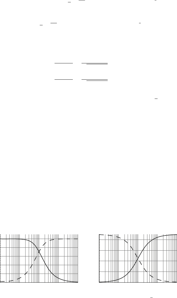
The absolute values and the phases of the transfer functions are shown in Fig. 6.7.
At the frequency
ω
0
= 1/
τ
, the input voltage is attenuated by 1/
√
2 ≈ 0.707 by
both filters. The CR filter attenuates frequencies
ω
<
ω
0
while high frequencies
are passing the circuit, so the CR circuit is called a high-pass filter. The RC circuit
passes low frequencies and attenuates high frequencies and is called a low-pass
filter. At the frequency
ω
0
, the phase shift between the input and the output voltage
is arctan(1)=
π
/4 = 45
o
.
From Eq. (6.4c,d) we know that the differentiation in the time domain corre-
sponds to a multiplication with s in the Laplace domain and that the integration in
the time domain corresponds to division by s in the Laplace domain. The transfer
function of a ‘differentiator’ or ‘integrator’ is therefore s or 1/s. The RC filter there-
fore becomes an integrator for large values of
τ
, or more precisely if the frequency
1/
τ
is much lower than all the frequencies contained in the signal. The CR circuit
approaches a differentiator if
τ
is small, i.e., if the frequency 1/
τ
is much higher
than the frequencies contained in the input signal.
To conclude this section we investigate the pole-zero and zero-pole filters shown
in Fig. 6.8, which are used extensively for signal shaping. The transfer functions of
the two filters are given by
0.01 0.1 1 10 100
0
20
40
60
80
Phase deg
CRRC
0.01 0.1 1 10 100
0
0.2
0.4
0.6
0.8
1
W
CRRC
ωτ
ωτ
Fig. 6.7 Absolute value and phase of the transfer function for an RC (low-pass) and a CR (high-
pass) filter. At the frequency
ω
0
= 1/
τ
the input voltage is attenuated by 1/
√
2 ≈ 0.707 and the
phase shift between the input and the output signal is
π
/4 = 45
o
190 6 Electronics for Drift Chambers
R
1
R
1
C
C
v(t)
v(t)
v
1
(t)
v
2
(t)
R
2
R
2
a)
b)
Fig. 6.8 Pole-zero (a) and zero-pole (b) filters used for unipolar shaping of exponential signals
W
PZ
(s)=
s + 1/
τ
1
s + 1/
τ
2
τ
1
= R
1
C
τ
2
=
R
1
R
2
R
1
+ R
2
C
τ
1
>
τ
2
(6.22)
and
W
ZP
(s)=
τ
1
τ
2
s + 1/
τ
1
s + 1/
τ
2
τ
1
= R
2
C
τ
2
=(R
1
+ R
2
)C
τ
1
<
τ
2
. (6.23)
Equations (6.22) and (6.23) are direct applications of the concepts presented in the
last paragraph of Sect. 6.1.1. The first filter is called pole-zero because the trans-
fer function has a single pole and a single zero, and the pole s = −1/
τ
2
is smaller
than the zero s = −1/
τ
1
of the transfer function. For the zero-pole filter the zero is
smaller than the pole. The transfer functions of both filters are shown in Fig. 6.9a.
The pole-zero filter passes low frequencies and attenuates high frequencies by
k = R
2
/(R
1
+ R
2
). The zero-pole filter attenuates low frequencies by a factor k and
passes high frequencies. At a frequency
ω
= 1/
√
τ
1
τ
2
the input voltage is attenu-
ated by
√
k for both filters, which is the geometric mean of the transfer functions at
zero frequency and infinite frequency.
Applying an exponential signal with time constant
τ
1
to the input of both fil-
ters with time constants
τ
1
and
τ
2
results in an exponential output signal with time
constant
τ
2
(Fig. 6.9b) [NIC 73]:
V(s)=L [e
−
t
τ
1
Θ
(t)] =
1
s + 1/
τ
1
V
1
(s)=W
PZ
(s)V (s)=
1
s + 1/
τ
2
. (6.24)
0.01 0.1 1 10 100
0
0.2
0.4
0.6
0.8
1
W
Pole Zero Zero Pole
1 2 3 4 5
0.2
0.4
0.6
0.8
1
Zero Pole
Pole Zero
t / τ
1
ω √(τ
1
τ
2
)
v
/
v
peak
0
Fig. 6.9 (a) Transfer functions of the pole-zero and zero-pole filter. (b) Output of both filters for
an input signal with the form exp(−t/
τ
1
). The output signal is an exponential with time constant
τ
2
, so the pole-zero filter shortens the exponential tail while the zero-pole filter lengthens the tail
6.1 Linear Signal Processing 191
Therefore the pole-zero filter is used for shortening exponential signal tails in
electronic circuits, and we also use it later to shorten the tail of wire chamber
signals.
For later use we give the delta response of the pole-zero filter, which evaluates to
w
PZ
(t)=L
−1
[W
PZ
(s)] =
δ
(t) −
τ
1
−
τ
2
τ
1
τ
2
e
−
t
τ
2
Θ
(t). (6.25)
As mentioned above, we only discuss transfer functions with real poles in this
book. A transfer function of this kind can be represented by a sequence of CR,
RC, pole-zero and zero-pole filters because the form given in Eq. (6.10) can
be interpreted as a product of suitably chosen transfer functions W
CR
, W
RC
,W
PZ
,
and W
ZP
.
6.1.4 Cascading of Circuit Elements
Let us assume two RC filters which are connected as shown in Fig. 6.10. An ap-
plication of the combination rules of the four impedances (Sect. 6.1.1) yields the
transfer function
V
2
(s)=
V(s)
(k + sRC)(1/k + sRC)
=
V(s)
(1+ sRC)
2
(6.26)
with k =(3 −
√
5)/2. The transfer function of two cascaded circuit elements is
therefore not simply equal to the product of the two individual transfer functions.
The reason is that the second RC filter takes current out of the first filter so that the
voltage at its output is no longer V
1
= 1/(1+ sRC)V(s).
In order to decouple the two circuits we must introduce a so-called voltage buffer
between them, which is an active device of infinite input impedance, infinite band-
width, and voltage gain G. Such a buffer produces an output signal which is an exact
copy of the input signal scaled by G. Owing to the infinite input impedance, no cur-
rent is taken out of the first RC circuit and the transfer function becomes the product
of the individual transfer functions. A realization of such a buffer was shown earlier
in Fig. 6.2a.
R
C
v(t)
v
2
(t)
v
1
(t)
v
3
(t)
v
1
(t)
R
C
R
C
v(t)
R
C
a)
b)
Fig. 6.10 (a) Series connection of two RC filters. As the second filter is ‘loading’ the first, the
transfer function is different from the product of the individual transfer functions. (b)TwoRC
filters separated by a voltage buffer of infinite input impedance. For this setup the transfer function
is given by W(s)=W
RC
(s)W
RC
(s)

192 6 Electronics for Drift Chambers
We conclude that a cascade of circuit elements with individual transfer functions
W
1
(s),W
2
(s)...W
n
(s), which are decoupled by ideal voltage buffers, has a transfer
function equal to the product
W(s)=W
1
(s) ×W
2
(s) ×...×W
n
(s). (6.27)
6.1.5 Amplifier Types, Bandwidth, Sensitivity, and Ballistic Deficit
The practical realizations of linear signal processing systems discussed above are
amplifiers and filter circuits connected to the detector electrodes. Parameters that
characterize these devices, such as gain and bandwidth, have a range of differing
definitions in the literature on microelectronics. We therefore review and define the
vocabulary for the discussion of detector electronics.
Bandwidth Limit: In the frequency domain, an amplifier is characterized by the
gain |W(i
ω
)| and the phase shift arg[W (i
ω
)] for each frequency. The bandwidth
limit of an amplifier is defined as the frequency at which the signal transmission has
been reduced by 3 dB from the central or midrange reference value. Since the power
level is defined as 10log(P/P
re f
) dB and the voltage level as 20log(V /V
re f
)dB,
a 3dB reduction corresponds to a power level of ≈ 0.5 and a voltage level equal
to ≈ 0.708 ≈ 1/
√
2 of the value at the centre frequency reference [MOT 93]. The
bandwidth limit of the RC low-pass filter is thus given by f
bw
= 1/2
πτ
= 1/2
π
RC.
Rise Time, Peaking Time: The rise time t
r
of a pulse is defined as the time taken
for its leading edge to rise from 10 to 90% of the peak height. The peaking time t
p
of a pulse is defined as the time taken for its leading edge to rise from zero to peak
height. When we talk about the peaking time of an amplifier we mean the peaking
time of its delta response.
Voltage, Current, and Charge Amplifiers: A voltage amplifier processes a
voltage signal presented at its input and is characterized by high input impedance.
A current amplifier processes the current signal flowing into the amplifier and is
characterized by low input impedance. The signals in wire chambers are induced
current signals, as discussed in the previous chapter. The example of the drift tube in
Sect. 5.6.1 shows that the detector capacitance C
det
together with the input resistance
R
in
forms an integration stage with bandwidth limit of f
bw
= 1/2
π
R
in
C
det
, which is
undesirable if one wants to preserve the fast signal. In order to preserve the chamber
signal shape, the input impedance of the amplifier must be small compared to all
other impedances in the detector or in the ideal case, equal to zero, which means
that we use current amplifiers for readout of wire chambers. If the bandwidth of
the current amplifier is such that it integrates a significant fraction of the chamber
signal, or the entire chamber signal, it is usually called a charge amplifier.
Sensitivity of Current and Charge Amplifiers: The filters discussed in the
previous sections transform an input voltage signal to an output voltage signal, and
therefore the dimension of the transfer function is [W(s)] = 1. The transfer function
of a current amplifier that transforms a current input signal into a voltage output
signal can be written as V(s)=kW (s)I(s), where k has dimensions of V/A=
Ω
and

6.1 Linear Signal Processing 193
W(s) keeps the dimension 1. In the time domain the relationship between the input
and output signals is
v(t)=k
w(t −t
)i(t
)dt
= kw(t
p
)
w(t −t
)
w(t
p
)
i(t
)dt
= g
h(t −t
)i(t
)dt
.
(6.28)
The value w(t
p
) is the peak of the delta response w(t), and the dimensionless func-
tion h(t) is the normalized delta response. An input current pulse of i(t)=Q
δ
(t)
results in an amplifier output peak voltage of v(t
p
)=gQ. We call g which has the
dimension V/C, the sensitivity of the amplifier, Typical wire chamber amplifiers
have sensitivities in the range of 1–50 mV/fC.
Ballistic Deficit: If a current amplifier has a peaking time t
p
which is much
longer than the duration of the input current signal i(t), the convolution integral can
be approximated and the output pulse is given by
v(t)=g
h(t −t
)i(t
)dt
≈ gh(t)
i(t
)dt
= gh(t)Q
tot
. (6.29)
The peak of the output signal is gQ
tot
. The output pulse height is therefore propor-
tional to the total signal charge and such an amplifier is called a charge amplifier.
For timing purposes or due to high signal rates, one typically wants to preserve the
signal speed and keep the pulse width to a minimum. Although the amplifiers used
for wire chambers will always have peaking times shorter than the maximum drift
time of the ions, an amplifier that integrates a significant fraction of the induced
charge is traditionally still called a charge amplifier.
As long peaking times limit the rate capability of a detector one usually has to
live with a compromise between pulse-width and charge measurement accuracy.
The incomplete measurement of the signal charge is characterized by the so-called
ballistic deficit, which is defined as the difference between the amplifier output pulse
height for the input signal i(t) and the output pulse height if the entire input signal
charge Q
tot
=
i(t)dt is contained in a delta current pulse Q
tot
δ
(t).
Equivalent Block Diagram: In Sect. 6.1.1 we saw that the transfer function
W(s) of a linear electronic circuit is specified by an expression of the form
W(s)=A
(s −z
1
)(s −z
2
)...(s−z
n
)
(s −p
1
)(s −p
2
)...(s−p
m
)
. (6.30)
Let us now assume that we have defined such a transfer function and we want to
find an electronic circuit realization of it. As an example we assume that we want to
transform a voltage signal V
1
(s) by the transfer function
V
2
(s)=W(s)V
1
(s)=G
s +
α
(s +
β
)(s +
γ
)
V
1
(s), (6.31)
where
α
,
β
, and
γ
are positive and real. We can interpret W (s) as the product of a
pole-zero filter and an RC filter, so a possible realization of this transfer function
can be seen in Fig. 6.11, where a pole-zero and an RC filter are coupled by an
194 6 Electronics for Drift Chambers
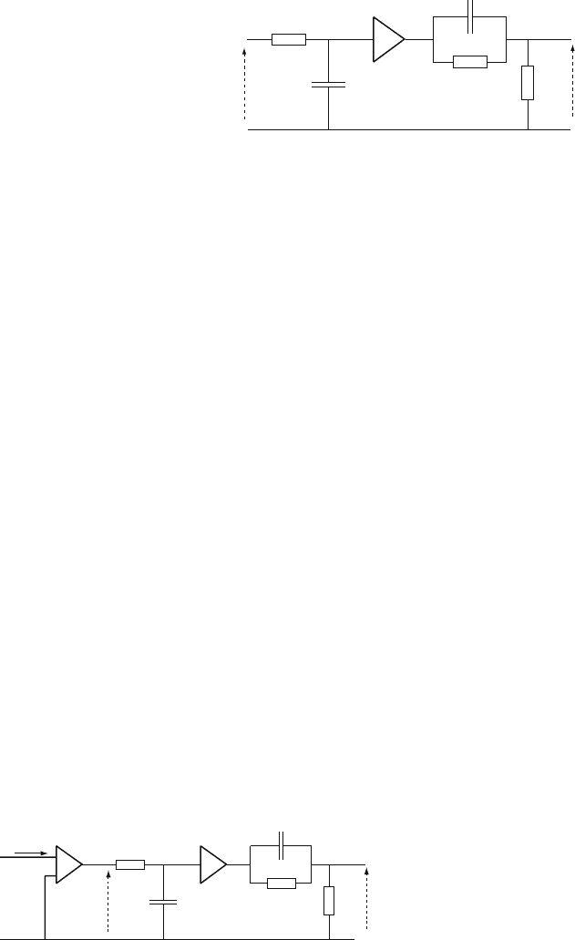
Fig. 6.11 Cascade of an RC
filter and a pole-zero filter
C
v(t)
v
1
(t)
R
2
R
1
R
C
G
ideal voltage buffer of gain G. Such a representation is of course not unique and
there are several ways to realize a transfer function. The important point is that any
transfer function can be represented by a cascade of simple, elementary circuits,
which facilitates the circuit analysis and serves as a basis for the actual design.
Up to now we have investigated filters that convert voltage input signals into volt-
age output signals. However, the signals induced on chamber electrodes are current
signals, so for our block diagram representation we need an idealized device which
converts a current input signal into a voltage signal. We assume an idealized device
with infinite bandwidth such that for a current input signal i(t) we get a voltage
output signal v(t)=ki(t). With this device we can complete our block diagram rep-
resentation of the detector readout electronics (Fig. 6.12). In principle this kind of
block diagram can also be used for a practical realization, where the voltage buffer
and current to voltage converter are devices with a bandwidth that must be broader
than the bandwidth of the other circuit elements. Although most designs of chamber
electronics consist of cascaded blocks with intermediate buffers, there are numerous
different ways of realizing the individual transfer functions. As outlined earlier, the
goal of this chapter is not the design a practical realization of the readout electronics
but its precise specification. The block diagram defined above serves as a basis for
the circuit realization.
6.2 Signal Shaping
The transfer function W (s) of the readout electronics must be chosen in order to
optimize the measurement of the quantity of interest, such as signal charge or signal
time. For this discussion the electronics noise plays a key role, and we have to
characterize noise sources and apply the theory of optimum filtering. Parameters
R
1
R
2
C
R
C
v
1
(t)
G
k
i(t)
v(t)
=
k
i(t)
Fig. 6.12 An ideal current to voltage converter followed by a CR and pole-zero filter
6.2 Signal Shaping 195
to be considered for this optimization process are rate capability (pulse width) and
crosstalk as well as the practical aspects for the realization of the electronics.
In this section we first discuss two common examples of amplifier transfer func-
tions, a unipolar and bipolar shaper, and we discuss their characteristics as outlined
in the last section. After that we describe various techniques to remove the long
1/(t + t
0
) tail of wire chamber signals in order to avoid pileup of signals at high
rates.
6.2.1 Unipolar and Bipolar Signal Shaping
Two commonly used transfer functions for signal shaping, a so-called unipolar
shaper and bipolar shaper, are defined by
W
uni
(s)=kA
1
(1+ s
τ
)
n+1
W
bip
(s)=kA
s
τ
(1+ s
τ
)
n+1
. (6.32)
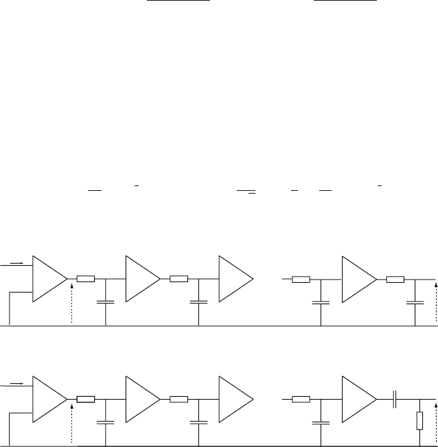
The equivalent block diagram of the unipolar shaper (Fig. 6.13a) consists of an
ideal current-to-voltage converter with equivalent resistance k followed by n + 1
RC filters. The filters are separated by n ideal voltage buffers with voltage gains
G
1
,G
2
...G
n
, which results in a gain factor of A = G
1
G
2
...G
n
. The bipolar shaper
uses n RC filters followed by a single CR filter, as shown in Fig. 6.13b. The delta
responses w(t) of the two shapers are calculated by performing the inverse Laplace
transforms of Eqs. (6.32), which are tabulated in standard textbooks [OPP 97]. Writ-
ing w(t)=gh(t), with the peak of h(t) normalized to unity, we find
h
uni
(t)=e
n
t
n
τ
n
e
−
t
τ
Θ
(t) h
bip
(t)=
e
r
√
n
n −
t
τ
t
r
τ
n−1
e
−
t
τ
Θ
(t) (6.33)
k
1
R
C
i(t)
i(t)
v
=
k i(t)
R
C
R
C
....
v(t)
v(t)
2n
n+1
R
C
a)
1
R
C
R
C
R
C
....
2n
R
C
k
v
=
k i(t)
b)
G
1
G
1
G
2
G
2
G
n
G
n
Fig. 6.13 (a) Unipolar shaping circuit consisting of n + 1 identical RC filters which are separated
by ideal voltage buffers. (b) Bipolar shaping circuit consisting of n identical RC filters and a single
CR filter with the same time constant
196 6 Electronics for Drift Chambers
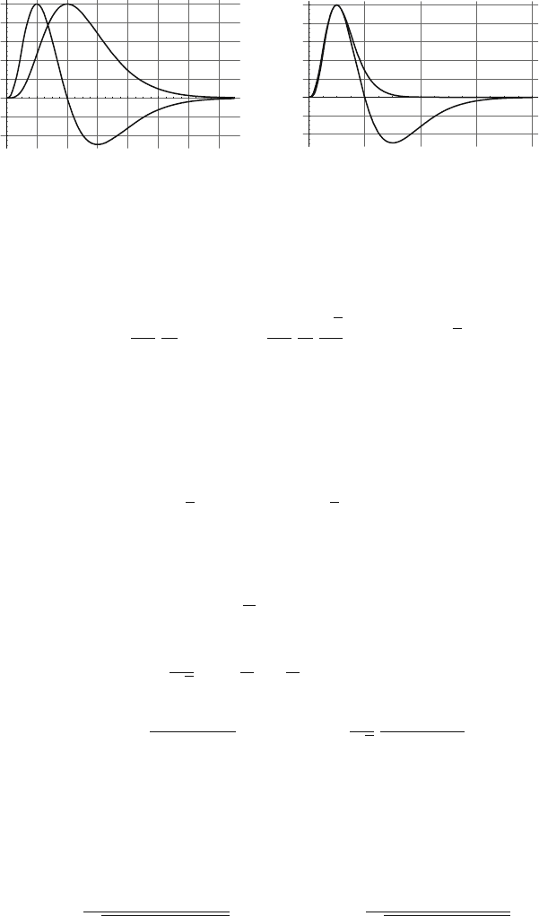
2 4 6 8 10 12 14
0.2
0.4
0.6
0.8
1
(a) (b)
2 4 6 8
–0.4
–0.2
–0.4
–0.2
0.2
0.4
0.6
0.8
1
t
/
t
p
t
/
τ
0
0
Fig. 6.14 Delta response for an unipolar shaper consisting of five RC filters and a bipolar shaper
consisting of four RC filters and a single CR filter. (a) The plot gives the delta responses for the
same value of
τ
and shows that the bipolar response is the derivative of the unipolar response.
(b) The plot shows the two delta responses with the same peaking time
with the sensitivity
g
uni
=
kA
τ
n!
n
n
e
n
g
bip
=
kA
τ
n!
r
n
e
r
√
n
r
r = n−
√
n. (6.34)
Figure 6.14a shows the two delta responses for n = 4. The unipolar shaper has a
peaking time of t
p
= n
τ
. Mathematically the bipolar delta response is the derivative
of the unipolar response, because W
bip
(s)=
τ
sW
uni
(s) and a multiplication with s
in the Laplace domain corresponds to a derivative in the time domain [Eq. (6.4c)].
Thus the bipolar delta response crosses the zero line at t = n
τ
. The peak and the
minimum of the bipolar delta response are situated symmetrically around the zero
crossing time at t
p
=
τ
(n−
√
n) and t
m
=
τ
(n+
√
n). If we want the peaking time t
p
of the two shapers to be equal we have to use the RC time constant
τ
= t
p
/n for the
unipolar shaper and
τ
= t
p
/r for the bipolar shaper.
h
uni
(t)=
t
t
p
n
e
n(1−t/t
p
)
Θ
(t), (6.35)
h
bip
(t)=
1
√
n
n −
rt
t
p
t
t
p
n−1
e
r(1−t/t
p
)
Θ
(t), (6.36)
H
uni
(s)=
t
p
e
n
n!
(n + st
p
)
n+1
H
bip
(s)=
1
√
n
st
2
p
e
r
n!
(r + st
p
)
n+1
. (6.37)
Here we have used the symbols H(s) to represent the Laplace transforms of the
delta responses h(t) normalized to unity at the peak. Figure 6.14b shows the two
delta responses with identical peaking times and n = 4.
The absolute value of the transfer function for the two shapers with a peaking
time t
p
is given by
|W
uni
(i
ω
)| =
kA
"
+
1+
ω
2
t
2
p
/n
2
,
n+1
|W
bip
(i
ω
)| =
kA
ω
t
p
/r
"
+
1+
ω
2
t
2
p
/r
2
,
n+1
. (6.38)