Blum W., Riegler W., Rolandi L. Particle Detection with Drift Chambers
Подождите немного. Документ загружается.

5.7 Signals Induced in Multiwire Chambers 177
Γ(λ)
λ
Gauss
Gatti
0
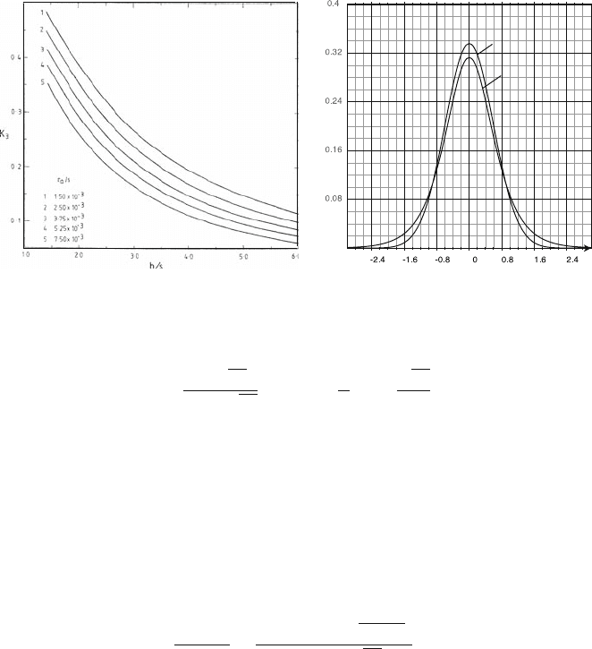
Fig. 5.15 (a) Values of the parameter K
3
as a function of chamber geometrical parameters h/s
and a/s [MAT 84b]. (b) Cathode charge distribution
Γ
(
λ
) according to Gatti for h/s = 2and
a/s = 5.25×10
−3
together with a Gaussian that has the same area and the same FWHM
K
1
=
K
2
√
K
3
4atan
√
K
3
K
2
=
π
2
1−
√
K
3
2
. (5.58)
Γ
(
λ
) represents the charge distribution on one of the cathode planes originating
from a single avalanche. We take it to be independent of direction in that plane,
the variable
λ
= x/h representing one coordinate in that plane, normalized to the
anode-cathode distance h. The other coordinate, at right angles to x, has already
been integrated over, following the idea of a cathode segmented into strips. One
of the two curves in Fig. 5.15b is Eq. (5.57) with a choice of K
3
indicated in the
caption. The other is a Gaussian for comparison, with the same area and the same
width. Gatti’s curve has a longer tail at large |
λ
|. The FWHM of the distribution can
be expressed as
FWHM
h
=
4arctanh(1/
√
2+ K
3
)
π
(1−0.5
√
K
3
)
. (5.59)
Expression (5.57) is approximate in the sense that it neglects any influence of the
avalanche position around the wire if the avalanche develops on one side. But this
is not relevant unless electric signals are recorded that are so long that the ions have
moved beyond a few wire radii. In practical measurements of particle tracks there
are many avalanches that contribute to an electric signal. These are spread out along
the track, by diffusion and other effects (cf. Chap. 2). The average formula (5.57) is
then quite adequate to generate, perhaps in a simulation program, the true charge by
superposition of many
Γ
(
λ
i
) at the avalanche positions
λ
i
.
Precision measurements of charge distributions for different avalanche positions
around the wire were reported by Gordon and Mathieson [MAT 84a].
Varying the ratio of cathode separation to wire pitch h/s from 0.1 to ∞, the para-
meter K
3
assumes values between 0.1 and 1, which means that the FWHM assumes
values between 2.8h and 2.4h. For a strip of finite width w centred at position
λ
,we
get the signal I(t,
λ
,w) by integrating Eq. (5.56), and we find
178 5 Creation of the Signal
I(t,
λ
,w)=
λ
+w/2
λ
−w/2
dI
c1
(t,
λ
)d
λ
= I
c
(t)
λ
+w/2
λ
−w/2
Γ
(
λ
)d
λ
= I
c
(t) P
0
(
λ
), (5.60)
where
P
0
(
λ
)=
K
1
K
2
√
K
3
arctan
K
3
tanhK
2
(
λ
+
w
2
)
−arctan
K
3
tanhK
2
(
λ
−
w
2
)
.
(5.61)
We call P
0
(
λ
) the pad response function. The fact that the signal on the entire
cathode plane is equal to half the total cathode signal is verified by evaluating
lim
w→∞
P
0
(
λ
)=
1
2
. (5.62)
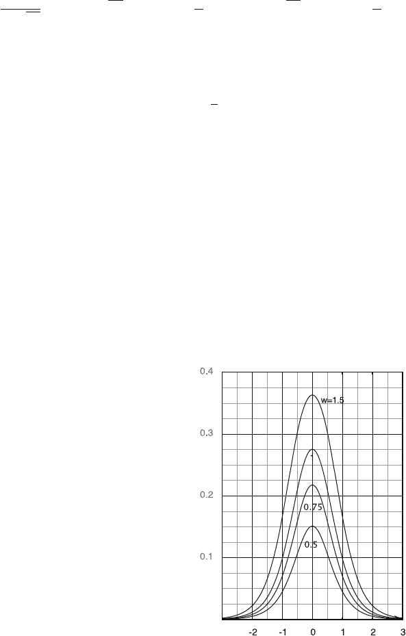
The pad response function depends on the strip width w. Figure 5.16 shows some
examples calculated for various w’s using the charge distribution displayed in
Fig. 5.15. The pad response function determines what fraction of the total cath-
ode signal is induced in the strip as a function of the distance between the centre
of the strip and the avalanche position (measured in the cathode plane). Equation
(5.62) implies that this fraction would reach 50% for an infinitely wide strip. For
narrower strips it is still quite large, the example of Fig. 5.16 shows that 22% is
collected when the avalanche is at the centre of a strip with width 0.75h and 11%
if it is over the centre of the neighbouring strip. For the measurement of tracks an
effective pad response function P
eff
(
λ
) is applicable, which results from folding in
the distribution of the positions of avalanches that contribute to the cathode strip
signal. This P
eff
(
λ
) can either be constructed using the methods described above
Fig. 5.16 Pad response
functions for four different
strip widths w in units of the
anode cathode distance h.
As w decreases, the curves
become smaller and thinner
λ
s
P
0
(λ
s
)
0

References 179
or be measured by fitting tracks. Often a simple superposition of Gauss curves is
sufficient.
The measurement of the coordinate of the avalanche is made by interpolating
the signals recorded on adjacent cathode strips with the help of the effective pad
response function P
eff
(
λ
). The strip width w and the cathode distance h have to be
chosen such that the typical pulse height induced on two or three adjacent strips falls
into the dynamic range of the readout electronics. If the resolution limit for position
determination along the wire is given by the electronics pulse-height measurement, a
strip width near the cathode-anode distance (w ≈h) gives the best position resolution
[GAT 79]. When the coordinate of the avalanche is exactly in between two strips, it
induces two equal signals on them. If the avalanche is produced in correspondence
with the centre of one strip, it induces a large signal on it and two smaller signals on
the two adjacent strips. Typically one records two signals in the first case and three
in the second.
Measuring the signal I
1
(t) and I
2
(t) on two adjacent cathode strips of pitch w we
have the relations I
1
(t)/I
2
(t)=P
0
(
λ
)/P
0
(
λ
−w), which can be inverted to yield the
avalanche position
λ
. Measuring the signals on three adjacent strips over-constrains
the equation and leads to a further improvement of the position resolution. With
I
2
(t)
I
1
(t)
= p
1
=
P
0
(
λ
1
)
P
0
(
λ
1
−w)
I
2
(t)
I
3
(t)
= p
2
=
P
0
(
λ
2
)
P
0
(
λ
2
+ w)
(5.63)
we find
λ
1
and
λ
2
which determines the same avalanche position. Since the mea-
surement error is roughly inversely proportional to the recorded pulse height on the
outer strips, one may use the relative weights of p
2
1
and p
2
2
to estimate
λ
from the
two independent measurements
λ
=
1
p
2
1
+ p
2
2
(p
2
1
λ
1
+ p
2
2
λ
2
) (5.64)
In order to achieve a precise signal measurement, the readout electronics will use
a signal processing filter that optimizes the signal-to-noise ratio. Such a processing
chain leaves the ratio of signals on neighbouring strips unchanged as long as it is
the same for the strips involved.
Another common way of determining the avalanche position is to simply deter-
mine the centre of gravity of the strip charges or to apply a Gaussian type fit to the
measured charges [END 81]. All of these methods introduce systematic errors as a
function of the distance of the track from the strip centre (‘differential nonlinearity’),
but these can be corrected with suitable models.
References
[CHA 92] G. Charpak, Electronic Imaging of Ionizing Radiation with Limited Avalanches in
Gases, Nobel Lecture, Stockholm, December 8, 1992
[END 81] I. Endo et al., Systematic shifts of evaluated charge centroid for the cathode readout
multiwire proportional chamber, Nucl. Instr. Meth. Phys. Res. A 188, 51–58 (1981)
180 5 Creation of the Signal
[GAT 79] E. Gatti et al., Optimum geometry for strip cathodes or grids in MWPC for avalanche
localization along the anode wires, Nucl. Instr. Meth. Phys. Res. A 163, 83–92 (1979)
[GAT 82] E. Gatti, G. Padovini, V. Radeka, Signal evaluation in multielectrode radiation detec-
tors by means of a time dependent weighting vector, Nucl. Instr. Meth. Phys. Res. A
193, 651–653 (1982)
[JAC 75] See any introduction to electrostatics, for example J.D. Jackson, Classical Electrody-
namics, Ch. 2, 2nd edition (John Wiley and Sons. New York 1975)
[MAT 84a] J.S. Gordon and E. Mathieson, Cathode charge distributions in multiwire chambers, I.
Measurement and theory, Nucl. Instr. Meth. Phys. Res. A 227, 267–276 (1984)
[MAT 84b] E. Mathieson and J.S. Gordon, Cathode charge distributions in multiwire chambers,
II. Approximate and empirical formulae, Nucl. Instr. Meth. Phys. Res. A 227, 277–282
(1984)
[RAM 39] S. Ramo, Currents induced in electron motion, Proc. IRE 27, 584 (1939)
[RIE 04] W. Riegler, Extended theorems for signal induction in particle detectors, Nucl. Instr.
Meth. Phys. Res. A 535, 287–293 (2004)
[SAN 80] R. Santonico and R. Cardarelli, Development of Resistive Plate Counters, Nucl. Instr.
Meth. Phys. Res. A 187, 377–380 (1981)

Chapter 6
Electronics for Drift Chambers
The signals induced on the drift chamber electrodes must be processed by appro-
priate readout electronics. The design and specification of the electronic circuits
depend strongly on the detector application. For timing purposes one typically wants
fast amplifiers to reduce time walk effects. For applications where charge measure-
ment is required one prefers long integration times (slower amplifiers) in order to
integrate a large fraction of the detector signal. For high-rate applications, signal
tail cancellation and baseline restoration are important issues in order to avoid sig-
nal pileup and baseline fluctuations. The electronics noise level must be considered
as well as it determines the required chamber gas gain for the desired signal-to-noise
ratio.
The art and science of electronics is a universe of its own, and we cannot develop
the contents of this chapter from the basic principles as we have undertaken to do in
the other chapters of this book. Here it is our task to collect the concepts that allow
us to arrive at the electronics specifications for particular detector applications. The
numerous ways of realizing the actual circuits are also not part of this book. The
reader interested in a more detailed treatment of electronic signal processing may
want to consult the textbooks of Oppenheim and Willsky [OPP 97] (mathematical
tools), Nahvi and Edminster [NAH 03], Horowitz and Hill [HOR 89] (basic intro-
duction to electronic circuits), Nicholson [NIC 73] (nuclear electronics), Radeka
[RAD 88] (low noise techniques), and Rehak [REH 83] and Gatti [GAT 85] (signal
processing for particle detectors).
The front-end electronics of wire chambers, or at least their first stages, are typ-
ically linear signal processing devices. A linear signal processing device has the
property that a given input pulse shape I
in
(t) results in an output pulse shape V
out
(t)
which is independent of the signal amplitude, i.e., V
out
[c ×I
in
(t)] = c ×V
out
[I
in
(t)]
for any value of the constant c.
There are important advantages of linearity: in position-sensitive wire cham-
bers with cathode segmentation for cathode charge interpolation (Sect. 5.7.2), the
track position is determined by the ratio of the charges induced on neighbouring
strips or pads. If the readout electronics were nonlinear, one would have to apply
a pulse-height-dependent correction of the position, which is undesirable. Another
W. Blum et al., Particle Detection with Drift Chambers, 181
doi: 10.1007/978-3-540-76684-1
6,
c
Springer-Verlag Berlin Heidelberg 2008
182 6 Electronics for Drift Chambers
compelling reason for linearity is related to signal shaping. The long 1/(t + t
0
) tail
of the wire chamber signal leads to signal pileup and hence to rate limitations. For
this reason one introduces filters (shapers) which reduce the pulse width. If the am-
plifier stages preceding the shaper are nonlinear, the signal shapes arriving at the
shaper vary according to their amplitude, which makes the shaper circuit with fixed
parameters inefficient. For linear electronics the shaper just has to be matched to the
input pulse shape, i.e., to the parameter t
0
for the given wire chamber geometry.
An amplifier is traditionally considered a device that produces an amplified copy
of the input signal. For example, the output of an ideal voltage amplifier for an
input voltage signal v
in
(t) is v
out
(t)=G ×v
in
(t), where G is the (dimensionless)
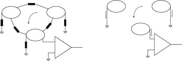
voltage gain of the amplifier. Figure 6.1a shows how a voltage signal induced on a
detector electrode is read out by a voltage amplifier. In order to create an exact copy
of the induced voltage signal the input impedance of the voltage amplifier must be
infinite, because for finite input impedance we would find a current flowing into the
amplifier, which would change the voltage V
3
(t).
Figure 6.1b shows a set of grounded electrodes where the moving charge in-
duces currents. Such a current can be read out by an ideal current-sensitive amplifier,
which produces an output voltage signal v(t)=ki
3
(t). The ‘gain’ k has the dimen-
sion of
Ω
and it would be more precise to call this device a current-to-voltage
converter. The input impedance of the device must be zero so that the electrodes
stay at ground potential.
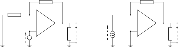
Figure 6.2 shows the realization of voltage and current amplifiers using an op-
erational amplifier, which is a device with very high voltage gain, very high input
impedance, and very high bandwidth, ideally all being infinite. The voltage am-
plifier shown in Fig. 6.2a has a gain of G = V
2
/V
1
= 1 + R
2
/R
1
and infinite input
impedance. The output voltage V
2
is independent of the load R
L
. The current ampli-
fier shown in Fig. 6.2b has a gain of k = V
2
/I
1
= −R and zero input impedance. Also
for this device the output voltage V
2
is independent of the load R
L
.Ifwewerejust
interested in a copy of the induced signal, the electronics chapter of this book would
end at this point. In practice the induced signal must be processed and transformed
by several filters in order to arrive at a useful signal-to-noise ratio, pulse width,
and frequency spectrum of the output signal, because these quantities determine the
q
x(t)
k
V
1
(t) V
2
(t)
Q
1
(t)
l
1
(t)
l
2
(t)
l
3
(t)
Q
2
(t)
Q
3
(t)
V(t)
= GV
3
(t)
V(t)
= kl
3
(t)
V
3
(t)
q
x
0
(t)
0
0
0
0
00
Z
12
Z
11
Z
13
Z
33
Z
in
= ∞
Z
in
= 0
Z
23
Z
22
G
a) b)
Fig. 6.1 (a) An ideal voltage amplifier with gain G and infinite input impedance reading the voltage
signal induced on the detector electrode. (b) An ideal current amplifier with conversion factor k
and input impedance zero reading the current signal induced on the detector electrode
6.1 Linear Signal Processing 183
+
–
+
–
V
1
(t)
R
1
R
2
R
L
+
–
I
1
(t)
R
R
L
a) b)
V
2
(t) V
2
(t)
Fig. 6.2 Realization of a voltage amplifier (a) and a current amplifier (b) by using an operational
amplifier
charge measurement accuracy, the rate capability, and the crosstalk behaviour of the
detector.
The signal filtering is also called signal shaping, and the readout electronics are
sometimes separated into an ‘amplifier’ and a ‘shaper’. In the following chapters
we only use the word ‘amplifier’ for the entire linear signal processing chain of the
readout electronics.
We conclude this introduction by noting that the vocabulary and tradition in the
field of detector electronics is somewhat different from the sometimes more familiar
field of radio and telecommunication electronics. Whereas the latter is formulated
almost exclusively in the frequency domain, detector signals are mostly discussed
in the time domain. For detector signals we are interested in pulse height, signal-
to-noise ratio, pulse width, signal pileup, and rate capability. All these numbers
are associated with the amplitude and time dependence of detector signals. In the
frequency domain the effect of a filter applied to a signal is simply the product of the
signal and the filter transfer function. The equivalent operation in the time domain is
the convolution of the input signal with the amplifier delta response. As we discuss
mostly time domain signals we make frequent use of the convolution integral.
Before describing the readout electronics we review the necessary vocabulary
and mathematical tools required for analysis of linear signal processing devices.
6.1 Linear Signal Processing
The Laplace and Fourier transformations of time domain signals are essential tools
for electrical circuit analysis. The following section summarizes the principal re-
lationships and examples that are used for later discussion of the actual front-end
electronics. Details of these techniques can be found in numerous textbooks; we
follow the nomenclature and definitions given in [OPP 97].
6.1.1 Laplace and Fourier Transforms
The Laplace transform of a time-dependent function f (t) is defined by
L [ f (t)] = F(s)=
∞
−∞
f (t) e
−st
dt, (6.1)

184 6 Electronics for Drift Chambers
where s is a complex number with real part
σ
and an imaginary part
ω
: s =
σ
+ i
ω
.
This definition is called the ‘bilateral’ Laplace transform because the integration ex-
tends from −∞ to ∞. In the case where f (t)=0fort < 0 the transform is equal to the
unilateral Laplace transform, which has a lower integration limit of 0. While F(s)
has no direct physical interpretation, the Fourier transform of the signal, defined by
F [ f (t)] =
∞
−∞
f (t) e
−i
ω
t
dt = F(i
ω
)
ω
= 2
π
f, (6.2)
expresses the signal as a superposition of sinusoidal waves of frequency f with am-
plitudes |F(i
ω
)| and relative phases arg[F(i
ω
)]. The Fourier transform is a special
case of the bilateral Laplace transform with
σ
= 0. The inverse transforms are
f (t)=
1
2
π
i
σ
+i∞
σ
−i∞
F(s)e
st
ds f(t)=
1
2
π
∞
−∞
F(i
ω
)e
i
ω
t
d
ω
. (6.3)
The transformations of the most common functions are tabulated in standard text-
books. For the Laplace and Fourier transforms, the following relations hold (proofs
can be found in [OPP 97]):
(a) Addition (b) Convolution
L [af(t)+bg(t)] = aF(s)+bG(s) L
(
∞
−∞
f (t −t
)g(t
)dt
)
= F(s)G(s)
(c) Time differentiation (d) Time integration
L
f
(n)
(t)
= s
n
F(s) L
(
t
−∞
f (t
)dt
)
=
1
s
F(s)
(e) Time shift (f) Time scaling
L [ f (t −t
0
)] = F(s)e
−st
0
L [ f (at)] =
1
a
F(
s
a
)
(g) Damping (h) Multiplication
L [e
−s
0
t
f (t)] = F(s + s
0
) L [t
n
f (t)] = (−1)
n
F
(n)
(s)
(i) Initial value if f (t)=0fort < 0 (j) Final value
f (0
+
)=lim
s→∞
sF(s) f (∞)=lim
s→0
sF(s)
(k) Parseval’s theorem
∞
−∞
f (t)
2
dt =
∞
−∞
|F(i2
π
f )|
2
df = 2
∞
0
|F(i2
π
f )|
2
df
(6.4)
The usefulness of these transformations for electrical circuit analysis is illustrated
by the following example. The voltage v
R
(t) across a resistor R for an impressed cur-
rent i(t) is given by Ohm’s law as v
R
(t)=Ri(t). The voltage across a capacitor C for
an impressed current i(t) is v
C
(t)=1/C
i(t)dt. The voltage across an inductance
L for an impressed current i(t) is given by v
L
(t)=Ldi(t)/dt. Voltages and currents
in a circuit containing R,L, and C elements are determined by applying Kirchhoff’s
laws, which state that the sum of voltages in every loop must be zero and the sum
of the currents on every node must be zero. This analysis therefore leads to a set of
linear differential equations for the currents and voltages in the circuit.

6.1 Linear Signal Processing 185
Writing the above relations in the Laplace domain, we find V
R
(s)=RI(s),
V
C
(s)=I(s)/sC, and V
L
(s)=sLI(s), and the circuit relations become algebraic
equations. Instead of having to solve a set of coupled differential equations in the
time domain we just have to solve a set of linear algebraic equations in the Laplace
domain! In addition, owing to the theorems stated above, many signal manipulations
are strongly simplified when working in the Laplace domain.
Finally we define the impedance Z(s) of a circuit element as Z(s)=V(s)/I(s).
We find the impedance of Z
C
(s)=1/sC for a capacitor and Z
L
(s)=sL for an in-
ductor. In analogy to the resistance R
1
+ R
2
of two resistors switched in series, the
total impedance of two impedances Z
1
and Z
2
switched in series is Z
1
+ Z
2
.Like-
wise, the parallel application of the impedances gives a total impedance of Z
1
Z
2
/
(Z
1
+ Z
2
).
6.1.2 Transfer Functions, Poles and Zeros, Delta Response
We now want to read out the chamber output signal i(t) with a general linear signal
processing device. Such a signal is, e.g., the current signal i(t) of the drift tube
indicated in Fig. 5.10. A linear device is defined by the following property: if the
input signals i
1
(t) and i
2
(t) result in output signals v
1
(t) and v
2
(t), the input signal
i(t)=c
1
i
1
(t)+c
2
i
2
(t) will result in the output signal v(t)=c
1
v
1
(t)+c
2
v
2
(t).
The input and output signals of a linear, time-invariant, and causal device are
related by a differential equation of the following form:
a
0
v(t)+a
1
dv(t)
dt
+ ...+ a
m
d
m
v(t)
dt
m
= b
0
i(t)+b
1
di(t)
dt
+ ...+ b
n
d
n
i(t)
dt
n
, (6.5)
where the coefficients a and b are independent of time. The term ‘time-invariant’
describes the fact that the relation between input and output signals is independent
of time. For a ‘causal’ system the output signal v(t) is zero as long as the input
signal i(t) is zero.
Performing the Laplace transform and using Eq. (6.4c) transforms this equation
into an algebraic equation with the solution
V(s)=
b
0
+ b
1
s + ...+ b
n
s
n
a
0
+ a
1
s + ...+ a
m
s
m
I(s)=W(s)I(s), (6.6)
where we have defined L [i(t)] = I(s) and L [v(t)] = V(s). The function W(s) is
called the transfer function of the system and we see that the transfer function of a
linear time-invariant system can be expressed by the ratio of two polynomials in the
Laplace domain.
Setting s = i
ω
yields the transfer function in the Fourier domain and the relation-
ship between input and output signals is
V(i
ω
)=W(i
ω
)I(i
ω
). (6.7)

186 6 Electronics for Drift Chambers
Separating the signal I and the transfer function W into the absolute value and the
phase indicates how the frequencies contained in the input signal are separately
transformed in order to yield the output signal:
V(i
ω
)=|I(i
ω
)||W(i
ω
)|exp [iarg[I(i
ω
)] + iarg[W (i
ω
)]]. (6.8)
The sinusoidal components of the input signal I are scaled by |W| and phase shifted
by arg[W]. For very high frequencies the transfer function from Eq. (6.6) behaves as
|W(i
ω
)| =∝
ω
n−m
. (6.9)
A system where n > m is non-physical because it would result in infinite amplifi-
cation at infinite frequency. We can therefore state that for the transfer function of
a realistic linear device we have n ≤ m.Annth-order polynomial has n (real and
complex) roots, so the transfer function W (s) can be expressed as
W(s)=A
(s −z
1
)(s −z
2
)...(s−z
n
)
(s −p
1
)(s −p
2
)...(s−p
m
)
. (6.10)
The roots s = z
1
,z
2
...are the zeros of W(s) and s = p
1
, p
2
...are the poles of W(s).
In general, z
i
and p
i
are complex numbers, and some of the roots may be repeated.
In the Laplace domain, the transfer function of a linear signal processing device can
therefore be fully described by its poles, its zeros, and a constant gain factor A.
A unit input signal I(s)=1 will result in the output signal V(s)=W (s).Re-
turning to the time domain we have L
−1
[1]=
δ
(t) and L
−1
[W(s)] = w(t).The
inverse Laplace transform of the transfer function is thus the output signal for a unit
delta input signal, which we call the delta response of the system. Since, according
to Eq. (6.4b), a multiplication in the Laplace domain corresponds to a convolution
in the time domain, in the latter Eq. (6.6) reads as
v(t)=
∞
−∞
w(t −t
)i(t
)dt
. (6.11)
If w(t) and i(t) are causal, meaning that w(t)=i(t)=0fort < 0, the convolution
integral reads as
v(t)=
t
0
w(t −t
)i(t
)dt
. (6.12)
The transfer function W(s) and the delta response w(t) are two equivalent ways of
describing a linear system, and this is symbolized in Fig. 6.3. Using partial fraction
expansion, we can write the transfer function W (s) in Eq. (6.10) with m ≥ n as a
sum of terms with the form 1/(s − p
i
)
k
i
, where k
i
≥ 0 are integers and the poles
are complex numbers (p
i
= a
i
+ ib
i
). The delta response w(t) of a linear system
therefore becomes a sum of terms with the form
L
−1
1
(s −p
i
)
k
i
=
t
k
i
−1
(k
i
−1)!
e
a
i
t
[cos(b
i
t)+isin(b
i
t)]
Θ
(t) k
i
≥ 1. (6.13)