Blum W., Riegler W., Rolandi L. Particle Detection with Drift Chambers
Подождите немного. Документ загружается.

5.6 Signals Induced on Electrodes Connected with Impedance Elements 167
00
0
V
1
ind
(t)
q
x(t)
0
0
0
Z
11
Z
33
Z
22
Z
12
Z
13
Z
23
a) b)
V
2
ind
(t)
V
3
ind
(t)
V
1
ind
(t)
V
2
ind
(t)
V
3
ind
(t)
I
1
ind
(t)
I
2
ind
(t)
I
3
ind
(t)
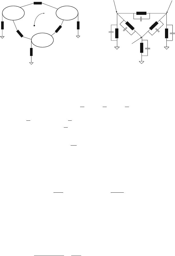
Fig. 5.9 (a) The point charge q induces voltages on the electrodes that are connected with
impedance elements. (b) These induced voltages are calculated by adding the mutual
electrode-electrode capacitances C
nm
to the equivalent circuit and placing the currents, induced on
the grounded electrodes, as impressed current sources on the nodes
q
ψ
1
(x)+Q
1
V
w
= Q
1
V
ind
1
+ Q
2
V
ind
2
+ Q
3
V
ind
3
. (5.28)
The charges
Q
n
and voltages V
n
are related by the capacitance matrix of the
three-electrode system giving
Q
n
= c
1n
V
w
. Writing the same relations for the other
electrodes results in
Q
n
= −
q
V
w
ψ
n
(x)+
∑
m
c
nm
V
ind
m
,s (5.29)
where Q
n
, V
ind
n
, and
ψ
n
are the charge, voltage, and weighting potential of electrode
n. If the point charge q moves along the trajectory x(t) we find time-dependent
charges Q
n
on the electrodes, and their rate of change is
dQ
n
dt
= −I
ind
n
(t)+
∑
m
c
nm
dV
ind
m
dt
. (5.30)
The I
ind
n
(t) are the currents from Eq. (5.13) induced on the electrodes in the case
where they are grounded. The charges Q
n
can only change due to currents flowing
between the electrodes, i.e., dQ
n
/dt =
∑
m
I
nm
+I
nn
. These currents in turn are given
by the potential differences and connecting impedances, as defined in Eq. (5.24). In
the Laplace domain we therefore have
∑
m
(V
ind
m
−V
ind
n
)
Z
nm
+
V
ind
n
Z
nn
= −I
ind
n
+
∑
m
sc
nm
V
ind
m
→ (5.31)
I
ind
n
=
∑
m
(sc
nm
+ y
nm
)V
ind
m
or V
ind
n
=
∑
m
(sc + y)
−1
nm
I
ind
m
, (5.32)
where the admittance matrix y
nm
is defined in Eq. (5.26). The following is our final
result:

168 5 Creation of the Signal
The voltages V
ind
n
(t) induced by a moving charge on electrodes connected to
impedances Z
nm
(s) are determined by first using Ramo’s theorem to calculate the
currents induced on the grounded electrodes and placing them as ideal current
sources on an equivalent circuit diagram with admittance matrix sc
nm
+ y
nm
(s)
(Fig. 5.9b).
The additional admittance matrix elements sc
nm
are due to the mutual capaci-
tance between the electrodes. Inverting the relation (5.26) for y
c
nm
= sc
nm
,wesee
that the impedances corresponding to c
nm
are given by
Z
c
nm
=
1
sC
nm
with C
nn
=
∑
m
c
nm
C
nm
= −c
nm
n = m (5.33)
The C
nm
are the electrode capacitances, which must be distinguished from the capac-
itance matrix c
nm
in the same way that the impedances Z
nm
must be distinguished
from the impedance matrix z
nm
. The equivalent circuit for Eq. (5.32) is shown in
Fig. 5.9b. To calculate the induced voltages we compute the currents induced on
grounded electrodes with Ramo’s theorem and perform the next step of the calcula-
tion analytically or, e.g., with an analog circuit simulation program.
For the completion of our task we still have to specify the actual trajectory of
the moving charge, and we must find the numerical values of the capacitance matrix
elements. For this, the weighting fields known from Eq. (5.13) turn out to be use-
ful because they have a simple relation to the capacitance matrix as well as to the
trajectory-defining field E(x). If metal electrodes are set to voltages V
n
, the poten-
tial
ψ
(x) is uniquely defined by the requirements that it fulfils the Laplace equation
in the volume between the electrodes and that
ψ
(x)=V
n
on the electrode surfaces.
The potential
ψ
(x)=
∑
n
V
n
V
w
ψ
n
(x) (5.34)
satisfies these conditions because the weighting potentials
ψ
n
are equal to V
w
on
electrode n and zero on the other electrodes, and since such a solution is unique it
is the general solution of this problem. From this we immediately obtain the field
E(x) as a linear superposition of the weighting fields:
E(x)=
∑
n
V
n
V
w
E
n
(x). (5.35)
The surface charge density on a metal electrode is related to the electric field on
the surface by
σ
=
ε
0
|E|. The total charge on electrode n is therefore defined by the
integral over the electrode surface A
n
Q
n
=
ε
0
*
A
n
E(x)dA =
∑
m
V
m
V
w
*
A
n
E
m
(x)dA =
∑
m
c
nm
V
m
. (5.36)
As a result, the capacitance matrix elements are calculated to be
c
nm
=
ε
0
V
w
*
A
n
E
m
(x)dA . (5.37)
5.6 Signals Induced on Electrodes Connected with Impedance Elements 169
Knowing the weighting fields E
n
(x) is therefore sufficient to calculate the chamber
signals in four steps:
1. Using Eq. (5.35) we find the ‘real’ electric field in the chamber which determines
the particle trajectories.
2. The induced currents on grounded electrodes follow from Ramo’s theorem
[Eq. (5.13)].
3. The capacitance matrix c
nm
and capacitances C
nm
are calculated from Eqs. (5.37)
and (5.33).
4. These capacitance elements are added to the equivalent circuit and the induced
currents are impressed on the nodes as ideal current sources.
The calculation of the weighting fields and capacitance matrix is performed
analytically or with dedicated computer programs. The final step of placing the cur-
rents on the equivalent circuit diagram is usually done by analog circuit simulation
programs.
5.6.1 Application to a Drift Tube and its Circuitry
We now illustrate the above procedure by applying it to the drift tube shown in
Fig. 5.10a. For our example we use values of l = 100cm, tube radius b = 1.5cm,
and wire radius a = 25
μ
m.
We first have to calculate the electric field in the detector and determine the
ion trajectories, as done in Eq. (5.16). Next we calculate the weighting fields and
the induced current signals using Ramo’s theorem, which was done in Eq. (5.18).
In a third step we calculate the capacitance matrix of the tube using Eq. (5.37).
Electrode 1 (the wire) has an area of A
1
= 2a
π
l ˆr and electrode 2 (tube) has an
area of A
2
= −2b
π
l ˆr. With the weighting fields E
1
= V
w
/rln(b/a) ˆr (wire) and
E
2
= −V
w
/rln(b/a) ˆr (tube) we find
c
11
= c
22
= −c
12
= −c
21
=
2
πε
0
l
ln(b/a)
. (5.38)
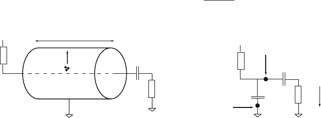
0
+U
R
in
R
L
0
C
a)
0
+U
R
in
R
L
0
C
b)
C
12
I
1
ind
(t)
–I
1
ind
(t)
Wire
Tu be
l
I
A
(t)
Fig. 5.10 (a) Typical setup for a drift tube. The wire is set to voltage U and is decoupled from the
amplifier input by a capacitor C. (b) The signals in the presence of the reactive elements are
calculated by placing the currents I
ind
n
(t), induced on the grounded electrodes, as ideal current
sources on the equivalent circuit

170 5 Creation of the Signal
The capacitances, calculated by Eq. (5.33), are therefore
C
11
= C
22
= 0 C
12
= C
21
=
2
πε
0
l
ln(b/a)
. (5.39)
For the chosen parameters we find C
12
= 20 pF. In the final step we impress the
induced currents as ideal current sources on the equivalent circuit of the tube as
shown in Fig. 5.10b. The wire is read out by an amplifier with input resistance
R
in
, which we choose to be 50
Ω
. In the equivalent circuit, the wire and the tube
have become pointlike nodes. This is only admissible if the tube is ‘electrically
short’, i.e., if the shortest wavelength
λ
= c/ f
0
processed by the readout electronics
with bandwidth limit f
0
is large compared to the tube length l. For the assumed
parameters this translates into f
0
300MHz. We use a value of 1.6 MHz in the
following. In a case where l is not much smaller than c/ f
0
we would have to consider
the tube to be a transmission line. In practical applications it is not convenient to set
the tube to negative high voltage −U, as shown in Fig. 5.6, but rather to ground the
tube and set the wire to positive voltage U. The signal −I
ind
1
induced on the tube can
be neglected because the current is ‘leaving’ to the ground node and is not entering
the amplifier.
Choice of the circuit parameters. The capacitor C decoupling the amplifier
from the potential U must be large compared to C
12
so that the current signal goes
into the amplifier instead of flowing into C
12
. But it must not be so large that the
energy E = CU
2
/2 it stores would destroy the amplifier in the case of a spark. Let
us take the typical value of 1 nF for C.
The resistor R
L
connects the wire to the voltage supply. It must be large in com-
parison to the impedance of C and R
in
in series so that only a small fraction of
the signal is lost into the power supply. If we want 99% of the bandwidth to find
this impedance sufficiently small, we may evaluate it at 1% of the bandwidth limit
leaving a value of
R
L
>
1
2
π
f
0
×0.01
+ R
in
≈ 10
4
Ω
(5.40)
in our example. In addition, this resistor is a source of thermal current noise which
is proportional to 1/
√
R
L
, so in this respect as well one chooses the resistor as large
as possible. The upper limit for R
L
is defined by the maximum voltage drop that
one allows for a given chamber current. With a primary ionization of, e.g., 125 elec-
trons and a gas gain of 5 ×10
5
at a rate of 100 kHz, we find a chamber current
of 1
μ
A, which leads to a tolerable voltage drop of 1 V for an R
L
value of 1M
Ω
.
Values for R
L
of 100 k
Ω
to several M
Ω
are typical; let us make R
L
= 1M
Ω
for
definiteness.
The relation between the induced current I
ind
1
and amplifier input current I
A
can
be determined by evaluating the equivalent circuit diagram in Fig. 5.10b. Using the
methods of Chap. 6 we change to the Laplace domain and find
I
A
(s)=
sR
L
C
1+ s(R
L
C + R
in
C + R
L
C
12
)+s
2
R
in
C
12
R
L
C
I
ind
1
(s). (5.41)
5.6 Signals Induced on Electrodes Connected with Impedance Elements 171
With the relative magnitudes of R
L
,R
in
,C, and C
12
that we assumed before, the
expression approximates to
I
A
(s) ≈
1
τ
2
1
s + 1/
τ
2
s
s + 1/
τ
1
I
ind
1
(s)
τ
1
= R
L
C = 1ms
τ
2
= R
in
C
12
= 1ns
. (5.42)
We can visualize the transfer function by an equivalent block diagram as outlined
in Chap. 6. Converting the current I
ind
1
to a voltage pulse, we see that this transfer
function corresponds to an RC integration element with time constant
τ
2
and a CR
differentiation element with time constant
τ
1
. This is illustrated in Fig. 5.11. The RC
integration with a time constant of
τ
1
=1 ns will change the ‘infinite’ rise time of the
induced signal to a signal with a rise time of ∼1ns, which has very little influence in
the case in which the amplifier rise time is longer than ≈ 10ns. The differentiation
with a time constant of
τ
2
= 1ms will also have very little influence on the signal
shape within the first several microseconds; it has, however, a profound influence
in the case of high-rate applications. Any voltage signal passing a capacitor will
integrate to zero, i.e.,
∞
0
I
A
(t)dt = 0. This means that the signal will slowly approach
zero and then have a very shallow and long undershoot with a timescale of several
times
τ
1
. If the counting rate is < 1/
τ
1
= 100Hz there is no mutual influence of the
pulses, but as the rate increases, more and more of these undershoots will pile up
and lead to baseline fluctuations. This point will be elaborated in Chap. 6, where
we discuss the amplifier transfer functions which shape the input signal I
A
so as to
obtain the optimum information from the detector signal.
5.6.2 Alternative Methods for the Calculation of the Signal
To conclude the discussion of signal theorems we point out that there is an alterna-
tive way of calculating the induced voltages for the setup of Fig. 5.9a, which does
not involve the four separate steps outlined earlier. Placing a delta current I
w
δ
(t) on
electrode n defines a time-dependent weighting field E
dyn
n
(x,t) in the space between
the electrodes, from which the voltage V
ind
n
(t) can be calculated by convolution with
the velocity vector of the moving charge [GAT 82]:
V
ind
n
(t)=−
q
I
w
t
0
E
dyn
n
[x(t
),t −t
] ˙x(t
)dt
. (5.43)
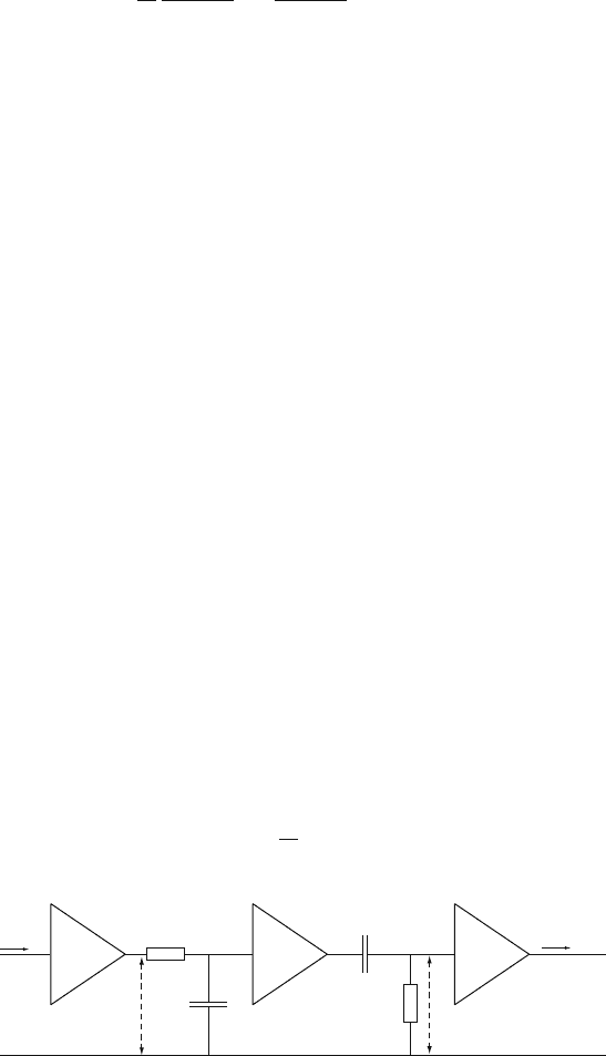
k
V – V
1/k
R
in
R
L
C
12
C
I
1
ind
(t)
I
A
(t)
=
1/k V
2
V
1
=
k I
1
ind
V
2
Fig. 5.11 Equivalent transfer function from the wire signal to the amplifier input
172 5 Creation of the Signal
This theorem can be useful when one studies a detector geometry with a simulation
program that allows the transient analysis of time-dependent electric fields.
There are detectors with electrodes that have only a finite conductivity, such as
resistive plate chambers (RPCs) [SAN 80] or undepleted silicon detectors. In such
cases, which do not normally occur in wire chambers, the theorems discussed in this
chapter are not directly applicable, but have to be generalized. An extension of the
theorems of signal generation including resistive electrodes as well as dissipative
dielectrics has been published elsewhere [RIE 04].
5.7 Signals Induced in Multiwire Chambers
A classical multiwire chamber consists of a plane of anode wires situated between
two parallel cathode planes. Often one of the cathode planes is subdivided into
strips orthogonal to the wires; then the avalanches can be localized in two dimen-
sions by reading out the electrical signals from the wires and the strips [GAT 79].
Such a geometry is depicted further on in Fig. 5.14. In the following we discuss the
main characteristics of the wire and cathode signals using the method outlined in
Sect. 5.1–5.4.
5.7.1 Signals Induced on Wires
The wire radii, typically 10–30
μ
m, are small compared to the distance between
the wires and the distance between the wire and the cathode of typically a few
millimetres. This fact gives rise to a coaxial electric field close to the wires, as we
show in the following. Setting the wires to potentials U
n
results in charges q
n
on the
wires, which are determined by the capacitance matrix through q
n
=
∑
N
m=1
c
nm
U
m
.
We combine the two cathode planes into electrode 1 and label the individual wires
as electrodes 2, 3, 4, etc. (cf. Fig. 5.12). We assume the wires to be infinitely long,
so c
nm
and q
n
are the capacitance matrix and charge per unit of wire length. The
electric field at a distance r from a line charge q is given by
E(r)=
q
2
πε
0
r
ˆr, (5.44)
cathode plane
anode wires
cathode plane
electrode ′1′
′2′
′3′′4′
′1′
Fig. 5.12 Electrode arrangement for which the induced currents are calculated in (5.48) to (5.51).
Wire ‘2’ carries the avalanche

5.7 Signals Induced in Multiwire Chambers 173
so at a point with distance r
1
and r
2
to two wires carrying charge q
1
and q
2
,the
electric field is E = 1/(2
πε
0
)([q
1
/r
1
] ˆr
1
+[q
2
/r
2
] ˆr
2
). In the vicinity of a wire,
meaning that r
1
r
2
, the field is dominated by the charge on this wire as long
as the charges q
1
and q
2
are of similar magnitude. We can conclude that the elec-
tric field at distance r from wire n is approximately coaxial, and its magnitude
given by
E(r)=
q
n
2
πε
0
r
=
1
2
πε
0
r
N
∑
m=1
c
nm
U
m
(5.45)
as long as r is small compared to the distance between the chamber electrodes. Un-
der these circumstances, the trajectory of the avalanche ions is just the same as the
one in the drift tube [Eq. (5.16)], and we have
r(t)=a
1+t/t
0
1
t
0
=
μ
a
2
πε
0
N
∑
m=1
c
nm
U
m
. (5.46)
It is interesting to note that it is the bandwidth of the electronics which decides
whether the coaxial approximation (5.45) is adequate. Imagine a fast amplifier (large
bandwidth) for signals only 50 ns long: with typical values of 1 ns for t
0
and 15
μ
m
for the wire radius a, the ions have travelled only a few percent of a typical wire pitch
of 1.5 or 2 mm, namely 0.1 mm in 50 ns – the coaxial approximation is probably
good enough in most circumstances. On the other hand, imagine a slower amplifier
(smaller bandwidth) for signals 1
μ
s long: with the same typical values the ions
have already travelled a significant fraction of the typical wire pitch, namely 0.5 mm
in 1
μ
s – the coaxial approximation is probably not good in many circumstances,
and the signal shape begins to depend on the angular distribution of avalanche ions
around the wire.
For the time being we wish to stay in the coaxial approximation (5.45) in order
to compute the signals on the various wires. We consider the situation with a plane
of anode wires, all on the same potential, between two cathode plates, as depicted
in Fig. 5.12.
Knowing the ion trajectory r(t) we need to calculate the weighting fields of
the wires in order to find the induced current signals. The weighting field of the
avalanche wire (electrode ‘2’), where the avalanche takes place, is found by setting
the wire to voltage V
w
and grounding all other wires and electrodes. This results in
the charge q
2
= c
22
V
w
on this wire, and the magnitude of the weighting field in the
coaxial approximation is
E
2
(r)=
c
22
V
w
2
πε
0
r
. (5.47)
The current induced by N
tot
ions of charge e
0
, moving away from the wire surface,
is therefore
I
2
(t)=−
N
tot
e
0
V
w
E
2
[r(t)]
dr
dt
= −
N
tot
e
0
4
πε
0
c
22
t + t
0
. (5.48)
The signal on the avalanche wire is negative because c
22
> 0 [cf. Eq. (5.6)].

174 5 Creation of the Signal
The weighting field of the closest neighbour (electrode ‘3’) is given by setting
wire ‘3’ to potential V
w
and grounding all other wires. This results in a charge of
q
3
= c
23
V
w
on the avalanche wire and the signal on wire ‘3’ is therefore
I
3
(t)=−
N
tot
e
0
4
πε
0
c
23
t + t
0
. (5.49)
The ‘cross-induced’ signal has the same shape as the signal on the avalanche wire
and because c
2n
< 0,n = 2, it is positive. The other wires have the same signal
polarity and shape, with relative amplitudes c
24
,c
25
, etc. We can express the relative
signal amplitudes by the more familiar capacitances C
nm
and find
I
n
(t)
I
1
(t)
=
c
2n
c
22
= −
C
1n
∑
N
m=1
C
2m
. (5.50)
The amplitude of the ‘cross-induced’ signal from the avalanche wire to wire n is
therefore given by the mutual capacitance between the avalanche wire and wire n
divided by the sum of all mutual capacitances of the avalanche wire to the other
electrodes.
We have to note that the capacitive coupling between wires causes a signal of
the same polarity on the neighbouring wires, which can be seen, e.g., by injecting a
wire signal with a pulse generator. During the early days of wire chamber develop-
ment one feared that the resolution of multiwire chambers was limited owing to this
capacitive coupling, which increases as the wire spacing is reduced. The opposite
polarity of the signal induced by the avalanche is, however, hiding this capacitive
crosstalk, which makes it ‘a simple matter to localize the wire which is the seed of
the avalanche, whatever the distance between the wires’ [CHA 92].
The sum of all wire signals is given by
I
w
(t)=
N
∑
n=2
I
n
(t)=−
N
tot
e
0
4
πε
0
1
t + t
0
N
∑
n=2
c
1n
= −
N
tot
e
0
4
πε
0
C
12
t + t
0
. (5.51)
Here we have used the relation C
12
= −c
12
and the fact that the two cathode
planes completely enclose the wires and the sum of all capacitance matrix elements
∑
N
m=1
c
nm
is zero. The sum of all wire signals thus has negative polarity. If all the
wires are set to the same voltage U, the characteristic time constant t
0
from Eq.
(5.46) assumes the form
1
t
0
=
μ
a
2
πε
0
U
N
∑
m=2
c
nm
=
μ
UC
12
a
2
πε
0
. (5.52)
For a comparison with the simple drift tube with wire radius a and tube radius
b, we remember that the wire signal and wire capacitance per unit length C
12
were
calculated [Eqs. (5.16), (5.18), (5.39)] to be
I(t)=−
N
tot
e
0
2ln(b/a)
1
t + t
0
1
t
0
=
2
μ
U
a
2
ln(b/a)
C
12
=
2
πε
0
ln(b/a)
. (5.53)
5.7 Signals Induced in Multiwire Chambers 175
If we express ln(b/a) by the capacitance per unit length C
12
the expression for the
wire signal in the drift tube is equivalent to the expression for the summed wire
signal in the MWPC. Therefore one can define the so called ‘equivalent cathode
radius’ for an MWPC as
b
eq
= aexp
2
πε
0
C
12
= aexp
55.6pF/m
C
12
. (5.54)
We can therefore conclude that while the avalanche ions are moving in the coax-
ial region of the wire, all signals in the wire chamber have the same shape, namely
hyperbolic proportional to 1/(t +t
0
) with the characteristic time constant t
0
.Therel-
ative amplitudes of the signals are determined by the capacitance matrix elements,
and the signal on the avalanche wire has negative polarity while all other signals
have positive polarity. For wire chambers where all wires are set to the same voltage
U, the summed wire signal is equivalent to the wire signal in a drift tube, and we
can define an equivalent cathode radius b
eq
for the wire chamber.
Finally, let us picture what we can expect beyond the coaxial approximation.
Once the avalanche ions are at a distance from the wire which is comparable to
the other chamber dimensions, the capacitance matrix elements are not sufficient to
determine the signals, the signal shapes differ, and the weighting fields for each wire
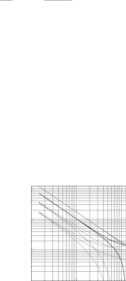
must be considered. The curves in Fig. 5.13 are the results of a numerical calculation
for a model chamber like the one in Fig. 5.12 with anode wires spaced 2.5 mm and
an anode-cathode distance of 5 mm. The weighting fields of the different electrodes
at the point of the travelling ions are represented as a function of the distance of the
ions from the wire that carries the avalanche. The ratios between the weighting fields
of different electrodes may be taken for the respective signal ratios. One observes
that the signal on the neighbouring wire ‘3’ (crosstalk) depends very much more on
the angular distribution of avalanches around their wire than is the case for the main
signal on electrode ‘2’.
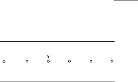
Fig. 5.13 Weighting fields
of different electrodes as a
function of the distance from
the centre of the avalanche
wire (‘2’) to the travelling
ions. The electrode numbers
characterize the source of the
weighting fields, the symbol
‘
Σ
’ referring to the sum of
all the wires. The various
branches in each group of
curves refer to different
directions the avalanche
might have around its wire:
perpendicular up and down
respective to the wire plane
andinthewireplane
10
–1
1
10
10
2
10
–2
10
–1
1
Distance (mm)
Electric Field (V/cm)
‘2’
‘1’
‘3’
‘Σ’
176 5 Creation of the Signal
5.7.2 Signals Induced on Cathode Strips and Pads
When the wires are enclosed by the two cathode planes, the sum of all chamber sig-
nals is zero at any time and the cathode signal I
c
(t) is equal to the negative summed
wire signal −I
w
(t). In our example, the cathodes are symmetrically placed with
respect to the wire plane, so the signal on a single cathode plane in the coaxial
approximation is
I
c1
(t)=
1
2
I
c
(t)=−
1
2
I
w
(t)=
1
2
N
tot
e
0
4
πε
0
C
12
t + t
0
. (5.55)
The avalanche can be localized in the direction perpendicular to the sense wire when
subdividing the cathode into separate strips or pads, as indicated in Fig. 5.14. The
weighting field of a cathode strip is calculated by setting the strip to potential V
w
while grounding all other strips and wires. This method is used in [MAT 84a] to ar-
rive at the exact expression for the weighting field and induced signal. For practical
purposes a few simplifications can be introduced [GAT 79][MAT 84b]. The signal
on a cathode strip is determined by first calculating the signal on a strip of infinites-
imal width, which is then integrated over the strip width w. This procedure defines
a so-called cathode charge distribution
Γ
(
λ
) through
dI
c1
(t,
λ
)=I
c
(t)
Γ
(
λ
)d
λ
∞
−∞
Γ
(
λ
)d
λ
=
1
2
, (5.56)
where
λ
= x/h is the distance of the infinitesimal strip from the avalanche posi-
tion. The distribution
Γ
(
λ
) can be calculated by investigating the weighting field
of an infinitesimal cathode strip. A single-parameter semi-empirical expression for
Γ
(
λ
) was given by Gatti et al. [GAT 79] and discussed by Mathieson and Gordon
[MAT 84b]:
Γ
(
λ
)=K
1
1−tanh
2
K
2
λ
1+ K
3
tanh
2
K
2
λ
. (5.57)
Here the parameters K
1
and K
2
are uniquely defined by K
3
, which depends on the
chamber geometry as shown in Fig. 5.15:
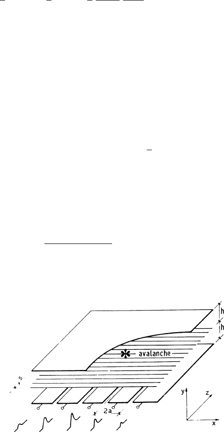
Fig. 5.14 Arowofwires
centred between two cathode
planes. By segmenting the
cathode into strips, the
position of the avalanche
along the wire direction can
be determined. The wire pitch
s,thestripwidthw = 2a,
and the distance h between
anode and cathode planes are
indicated