Bichop R.H. (Ed.) Mechatronic Systems, Sensors, and Actuators: Fundamentals and Modeling
Подождите немного. Документ загружается.

21-122 Mechatronic Systems, Sensors, and Actuators
21.5.8.1 Electromagnetic System Modeling in Microactuators with Permanent
Magnets: High-Fidelity Modeling and Analysis
In this section we focus our efforts to derive the expanded equations for the electromagnetic torque and
force on cylindrical permanent-magnet thin films, see Figure 21.135. The permanent-magnet thin film is
assumed to be uniformly magnetized and the equations are developed for two orientations of the mag-
netization vector (the orientation is parallel to the axis of symmetry, and the orientation is perpendicular
to this axis). Electromagnetic fields and gradients produced by the planar windings should be found at a
point in inertial space, which coincides with the origin of the permanent-magnet axis system in its initial
alignment. Our ultimate goal is to control microactuators, and thus, high-fidelity mathematical models
(which will result in viable analysis, control, and optimization) must be derived. To attain our objective,
the complete equations for the electromagnetic torque and force on a cylindrical permanent-magnet thin
films are found.
The following notations are used: A, R, and l are the area, radius, and length of the cylindrical permanent
magnet; B is the magnetic flux density vector; B
e
is the expanded magnetic flux density vector; [
∂
B] is
the matrix of field gradients [T/m]; [
∂
B
e
] is the matrix of expanded field gradients [T/m]; F and T are
the total force and torque vectors on the permanent-magnet thin film; i is the current in the planar
microwinding; m is the magnetic moment vector [A m
2
]; M is the magnetization vector [A/m]; r is the
position vector (x, y, z are the coordinates in the Cartesian system),
T
r
is the inertial coordinate vector-transformation matrix; W and Π are the work and potential energy;
θ
is the Euler orientation for the 3-2-1 rotation sequence; ∇ is the gradient operator; subscript ij represents
partial derivative of i component in j-direction; subscript (ij)k represents partial derivative of ij partial
derivative in k-direction;
–
(bar over a variable) indicates that it is referenced to the microactuator
coordinates.
21.5.8.2 Electromagnetic Torques and Forces: Preliminaries
The equations for the electromagnetic torque and force on a cylindrical permanent-magnet thin film are
found by integrating the equations for torques and forces on an incremental volume of the permanent-
magnet thin film with magnetic moment Mdv over the volume. Figure 21.135 illustrates the microactuator
with the cylindrical permanent-magnet thin film in the coordinate system, which consists of a set of
orthogonal body-fixed axes that are initially aligned with a set of orthogonal x-, y-, z-axes fixed in the
inertial space.
The equations for the electromagnetic torque and force on an infinitesimal current can be derived
using the fundamental relationship for the force on a current-carrying-conductor element in a uniform
magnetic field. In particular, for a planar current loop (planar microwinding) with constant current i in
the uniform magnetic field B (vector B gives the magnitude and direction of the flux density of the
external field), the force on an element dl of the conductor is found using the Lorentz force law
Assuming that the magnetic flux is constant through the magnetic loop, the torque on a planar current
loop of any size and shape in the uniform magnetic field is
r
x
y
z
=
F idlB×
l
°
=
T i r dlB×()×
l
°
i
rB⋅()dlBrdl⋅
l
°
–
l
°
==
9258_C021_Sect002-005.fm Page 122 Wednesday, October 10, 2007 7:10 PM
Actuators 21-123
Using Stokes’s theorem, one has
or
The electromagnetic torque T acts on the infinitesimal current loop in a direction to align the magnetic
moment m with the external field B, and if m and B are misaligned by the angle
θ
, we have
The incremental potential energy and work are found as
Using the electromagnetic force, we have
and
21.5.8.3 Coordinate Systems and Electromagnetic Field
The transformation from the inertial coordinates to the permanent-magnet coordinates is
We use the transformation matrix
If the deflections are small, we have
T i
dA ∇ rB⋅()B ∇ r×()dA⋅
s
°
–×
s
°
idAB×
s
°
==
T iAB× mB×==
TmB
θ
sin=
dW dΠ T d
θ
mB
θ
d
θ
and Wsin Π mB
θ
cos– mB⋅–== = == =
dW dΠ– F dr⋅∇Πdr⋅–== =
F ∇Π– ∇ mB⋅()m ∇⋅()B== =
r T
r
r =
θ
y
θ
z
coscos
θ
y
θ
z
sincos
θ
y
sin–
θ
x
θ
y
θ
z
θ
x
θ
z
sincos–cossinsin
θ
x
θ
y
θ
z
θ
x
θ
z
sincos+sinsinsin
θ
x
θ
y
cossin
θ
x
θ
y
θ
z
θ
x
sin
θ
z
sin+cossincos
θ
x
θ
y
θ
z
θ
x
θ
z
cossin–sinsincos
θ
x
θ
y
coscos
x
y
z
=
r
x
y
z
, r
x
y
z
==
T
r
=
θ
y
θ
z
coscos
θ
y
θ
z
sincos
θ
y
sin–
θ
x
θ
y
θ
z
θ
x
θ
z
sincos–cossinsin
θ
x
θ
y
θ
z
θ
x
θ
z
sincos+sinsinsin
θ
x
θ
y
cossin
θ
x
θ
y
θ
z
θ
x
θ
z
sinsin+cossincos
θ
x
θ
y
θ
z
θ
x
θ
z
cossin–sinsincos
θ
x
θ
y
coscos
T
rs
1
θ
z
−
θ
y
−
θ
z
1
θ
x
θ
y
θ
–
x
1
=
9258_C021_Sect002-005.fm Page 123 Wednesday, October 10, 2007 7:10 PM

21-124 Mechatronic Systems, Sensors, and Actuators
It should be emphasized that we use the 3-2-1 orthogonal transformation matrix for the z-y-x Euler
rotation sequence, and
θ
x
,
θ
y
,
θ
z
are the rotation Euler angle about the x, y, and z axes.
The field B and gradients of B produced by the microcoils fixed in the inertial frame and expressed
assuming that the electromagnetic fields can be described by the second-order Taylor series. Expanding
B about the origin of the x, y, z system as a Taylor series, we have [18]
or
where
We den ote
Then,
Hence, the first-order gradients are given as
The expanded field is expressed in the permanent-magnet coordinates as
where .
B
e
Br∇⋅()B
1
2
--
r ∇⋅()
2
B++=
B
ei
B
i
∂
B
i
∂
r
--------
r
1
2
--
r
T
∂
2
B
i
∂
r
2
----------
r++=
∂
B
i
∂
r
--------
∂
B
i
∂
x
--------
∂
B
i
∂
y
--------
∂
B
i
∂
z
--------
and
∂
2
B
i
∂
r
2
----------
∂
∂
B
i
∂
x
------
∂
x
---------
∂
∂
B
i
∂
x
------
∂
y
---------
∂
∂
B
i
∂
x
------
∂
z
---------
∂
∂
B
i
∂
y
------
∂
x
---------
∂
∂
B
i
∂
y
------
∂
y
---------
∂
∂
B
i
∂
y
------
∂
z
---------
∂
∂
B
i
∂
z
------
∂
x
---------
∂
∂
B
i
∂
z
------
∂
y
---------
∂
∂
B
i
∂
z
------
∂
z
---------
==
B
ij
∂
B
i
∂
j
--------
and B
ij()k
∂
∂
B
i
∂
j
------
∂
k
----------
==
∂
B
i
∂
r
--------
B
ix
B
iy
B
iz
[]and
∂
2
B
i
∂
r
2
----------
B
ix()x
B
ix()y
B
ix()z
B
iy()x
B
iy()y
B
iy()z
B
iz()x
B
iz()y
B
iz()z
==
B
eij
B
ij
∂
∂
B
i
∂
j
------
∂
r
----------
r+ B
ij [B
ij()x
B
ij()y
B
ij()z
]
r+==
B
e
Br∇⋅()B
1
2
--
r ∇⋅()
2
B++=
B T
r
B and ∇ T
r
∇==
9258_C021_Sect002-005.fm Page 124 Wednesday, October 10, 2007 7:10 PM
Actuators 21-125
Using r = , one has
and
21.5.8.4 Electromagnetic Torques and Forces
Now let us derive the fields and gradients at any point in the permanent magnet using the second-order
Taylor series approximation. To eliminate the transformations between the inertial and permanent
magnet coordinate systems and simplify the second-order negligible small components, we assume that
the relative motion between the magnet and the reference inertial coordinate is zero and the T
rs
trans-
formation matrix is used (otherwise, the second-order gradient terms will lead to cumbersome results).
The magnetization (the magnetic moment per unit volume) is constant over the volume of the
permanent-magnet thin films, and m = Mv.
Assuming that the magnetic flux is constant, the total electromagnetic torque and force on a planar
current loop (microwinding) in the uniform magnetic field is
where
Case 1: Magnetization Along the Axis of Symmetry
For orientation of the magnetization vector along the axis of symmetry (x-axis) of the permanent-magnet
thin films, we have
Thus, in the expression ,
T
r
T
r
B
ei
B
i
∂
B
i
∂
r
--------
T
r
T
r
1
2
--
r
T
T
r
∂
2
B
i
∂
r
2
----------
T
r
T
r++=
B
e
T
r
B
x
∂
B
x
∂
r
-------
T
r
T
r
1
2
--
r
T
T
r
∂
2
B
x
∂
r
2
---------
T
r
T
r++
B
y
∂
B
y
∂
r
-------
T
r
T
r
1
2
--
r
T
T
r
∂
2
B
y
∂
r
2
---------
T
r
T
r++
B
z
∂
B
z
∂
r
-------
T
r
T
r
1
2
--
r
T
T
r
∂
2
B
z
∂
r
2
---------
T
r
T
r++
=
TMB
e
r+× M ∇⋅()B
e
×()vd
v
=
FM∇⋅()B
e
vd
v
=
M ∇⋅()B
e
∂
B
e
[]M
B
exx
B
exy
B
exz
B
eyx
B
eyy
B
eyz
B
ezx
B
ezy
B
ezz
M
x
M
y
M
z
==
M ∇⋅()B
e
∂
B
e
[]M M
x
B
exx
B
exy
B
exz
==
T
v
(MB
e
r (M ∇⋅ )B
e
)×+× vd=
9258_C021_Sect002-005.fm Page 125 Wednesday, October 10, 2007 7:10 PM
21-126 Mechatronic Systems, Sensors, and Actuators
the terms are
Therefore,
and
The terms in the derived equations must be evaluated.
Let us find the analytic expression for the electromagnetic torque . In particular, we have
where
and
Therefore,
Furthermore,
Thus, for , one has
rM∇⋅()B
e
× M
x
B–
exy
zB
exz
y
+
B
exx
zB
exz
x–
−B
exx
yB
exy
x+
and MB
e
× M
x
0
B
ez
–
B
ey
==
T
x
M
x
B
exz
yB
exy
z–()vd
v
=
T
y
M
x
B
ez
vM
x
B
exx
zB
exz
x–()vd
v
+d
v
–=
T
z
M
x
B
ey
vM
x
B
exy
xB
exx
y–()vd
v
+d
v
=
T
x
B
exz
y vd
v
B
xz
y vB
xx()z
xy vB
xy()z
y
2
vB
xz()z
zy() vd
v
+d
v
+d
v
+d
v
=
y vd
v
0, xy vd
v
0, zy vd
v
0===
y
2
vd
v
y
2
ydzdxd
R
2
z
2
––
R
2
z
2
–
−R
R
1
2
--
l–
1
2
--
l
1
4
--
π
lR
4
1
4
--
vR
4
===
M
x
B
exz
yvd
v
M
x
1
4
--
B
xy()z
vR
4
=
M
x
B
exy
zvd
v
M
x
1
4
--
B
xy()z
vR
4
=
T
x
T
x
M
x
B
exz
yB
exy
z–()vd
v
M
x
1
4
--
B
xy()z
vR
4
1
4
--
B
xy()z
vR
4
– 0== =
9258_C021_Sect002-005.fm Page 126 Wednesday, October 10, 2007 7:10 PM
Actuators 21-127
Then, for , we obtain
Finally, we obtain the expression for T
z
as
Thus, the following electromagnetic torque equations result:
The electromagnetic forces are found as well. In particular, from
and
using the expressions for the expanded magnetic fluxes, e.g.,
and performing the integration, one has the following expressions for the electromagnetic forces as the
function of the magnetic field:
T
y
T
y
M
x
B
ez
dv M
x
B
exx
zB
exz
x–()dv
v
+
v
–=
M
x
B
z
B
zx()x
1
24
-----
l
2
B
zy()y
1
8
--
R
2
B
zz()z
1
8
--
R
2
+++v– B
xx()z
1
4
--
R
2
1
12
-----
l
2
– v+=
vM
x
B
z
B
xx()z
1
4
--
R
2
1
8
--
l
2
– B
yy()z
1
8
--
R
2
B
zz()z
1
4
--
R
2
+++–=
T
z
M
x
B
ey
dv M
x
B
exy
xB
exx
y–()dv
v
+
v
=
vM
x
B
y
B
xx()y
1
8
--
l
2
1
4
--
R
2
– B
yy()y
–
1
8
--
R
2
B
yz()z
–
1
8
--
R
2
+=
T
x
0=
T
y
vM
x
B
z
B
xx()z
1
4
--
R
2
1
8
--
l
2
– B
yy()z
1
8
--
R
2
B
zz()z
1
4
--
R
2
+++–=
T
z
vM
x
B
y
B
xx()y
1
8
--
l
2
1
4
--
R
2
– B
yy()y
1
8
--
R
2
B
yz()z
1
8
--
R
2
––+=
F
x
M
x
B
exx
vd
v
=
F
y
M
x
B
exy
vd
v
=
F
z
M
x
B
exz
vd
v
=
B
exx
vd
v
B
xx
B
xx()x
xB
xx()y
yB
xx()z
z+++()vd
v
=
F
x
vM
x
B
xx
, F
y
vM
x
B
xy
, F
z
vM
x
B
xz
===
9258_C021_Sect002-005.fm Page 127 Wednesday, October 10, 2007 7:10 PM
21-128 Mechatronic Systems, Sensors, and Actuators
Case 2: Magnetization Perpendicular to the Axis of Symmetry
For orientation of the magnetization vector perpendicular to the axis of symmetry, the following equation
is used to find the electromagnetic torque:
where
and
Thus,
Expressing the fluxes and performing the integration, we have the following expressions for the torque
components as the function of the magnetic field:
The electromagnetic forces are found to be
T (MB
e
rM∇⋅()B
e
)×+× vd
v
=
M ∇⋅()B
e
∂
B
e
[]M M
z
B
exz
B
eyz
B
ezz
rM∇⋅()B
e
× M
z
B–
eyz
zB
ezz
y+
B
exz
zB
ezz
x–
B
exz
yB
eyz
x+
===
MB
e
× M
z
B
ey
–
B
ex
0
=
T
x
M
z
B
ey
vM
z
B
exz
yB
eyz
z–()vd
v
+d
v
–=
T
y
M
z
B
ex
vM
z
B
ezz
zB
ezz
x–()vd
v
+d
v
=
T
z
M
z
B
eyz
xB
exz
y–()vd
v
=
T
x
vM
z
B
y
B
xx()y
1
24
-----
l
2
B
yy()y
1
8
--
R
2
B
yz()z
1
8
--
R
2
+++–=
T
y
vM
z
B
x
B
xz()y
3
8
--
R
2
1
12
-----
l
2
– B
xx()x
1
24
-----
l
2
B
xy()y
1
8
--
R
2
+++=
T
z
vM
z
B
xy()y
1
12
-----
l
2
1
4
--
R
2
–=
F
x
M
z
B
exz
dv
v
vM
z
B
xz
==
F
y
M
z
B
eyz
dv
v
vM
z
B
yz
==
F
z
M
z
B
ezz
dv
v
vM
z
B
zz
==
9258_C021_Sect002-005.fm Page 128 Wednesday, October 10, 2007 7:10 PM

Actuators 21-129
Thus, the expressions for the electromagnetic force and torque components are derived. These equa-
tions provide one with a clear perspective on how to model, analyze, and control the electromagnetic
forces and torques changing the applied magnetic field because the terms
can be viewed as the control variables. It must be emphasized that the electromagnetic field (B
ij
and B
(ij)k
)
is controlled by regulating the current in the planar microwindings and designing the microwindings
(or other radiating energy microdevices). As was discussed, the derived forces and torques must be used
in the torsional-mechanical equations of motion for the microactuator, and, in general, the six-degree-
of-freedom microactuator mechanical dynamics results. These mechanical equations of motion are easily
integrated with the derived electromagnetic equations, and closed-loop systems can be designed to attain
the desired microactuator performance. These equations guide us to the importance of electromagnetic
features in the modeling, analysis, and design of microactuators.
21.5.8.5 Some Other Aspects of Microactuator Design and Optimization
In addition to the electromagnetic-mechanical (electromechanical) analysis and design, other design and
optimization problems are involved. As an example, let us focus our attention on the planar windings.
The ideal planar microwindings must produce the maximum electromagnetic field, minimizing the
footprint area, taking into consideration the material characteristics, operating conditions, applications,
power requirements, and many other factors. Many planar winding parameters and characteristics can
be optimized, for example, the dc resistance must be minimized to improve the efficiency, increase the
flux, decrease the losses, etc. To attain good performance, in general, microwindings have the concentric
circular current path and no interconnect resistances. For N-turn winding, the total dc resistance r
t
is
found to be
where
ρ
is the winding material resistivity, t
w
is the winding thickness, r
Ok
and r
Ik
are the outer and inner
radii of the k-turn winding, respectively.
To achieve the lowest resistance, the planar winding radii can be optimized by minimizing the resis-
tance, and the minimum resistance is denoted as r
tmin
. In particular, making use of first- and second-
order necessary conditions for minimization, one has
where r
w
is the inner or outer radius of an arbitrary turn of the optimized planar windings from the
standpoint of minimizing the resistance.
Then, the minimum value of the microcoil resistance is given by
where r
OR
and r
IR
are the outer and inner radii of the windings (i.e., r
O Nth microcoil
and r
I 1st microcoil
),
respectively.
B
ij
∂
B
i
∂
j
--------
and B
ij()k
∂
∂
B
i
∂
j
------
∂
k
---------
==
r
t
2
πρ
t
w
----------
1
r
Ok
/
r
Ik
()ln
-------------------------
k=1
N
=
dr
t
dr
w
-------- 0 and
d
2
r
t
dr
w
2
--------
> 0=
r
tmin
2
πρ
t
w
----------
N
r
OR
/r
IR
()
--------------------
=
9258_C021_Sect002-005.fm Page 129 Wednesday, October 10, 2007 7:10 PM
21-130 Mechatronic Systems, Sensors, and Actuators
Thus, using the number of turns and turn-to-turn spacing, the outer and inner radii of the k-turn
winding are found as
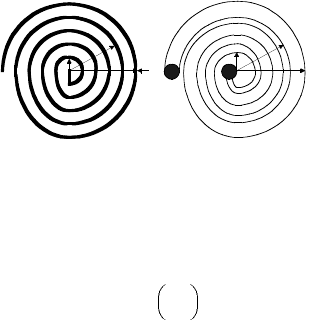
For spiral windings, the averaging (equivalency) concept should be used because the outer and inner
radii are the functions of the planar angle, see Figure 21.138. Finally, it should be emphasized that the
width of the Nth microcoil is specified by the rated voltage current density versus maximum current
density needed, fabrication technologies used, material characteristics, etc.
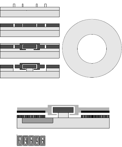
21.5.9 Micromachined Polycrystalline Silicon Carbide Micromotors
Articles [19,20] report the silicon-based fabrication of reluctance micromotors. This section is focused
on a new enabling technology to fabricate microtransducers. Multilayer fabrication processes at low
temperature and micromolding techniques were developed to fabricate SiC microstructures and salient-
pole micromotors, which can be used at a very high temperature (400°C and higher) [21,22]. This was
done through the SiC surface micromachining. Advantages of the SiC micromachining and SiC technol-
ogies (high temperature and ruggedness) should be weighted against fabrication drawbacks because new
processes must be designed and optimized. Reactive ion etching is used to pattern SiC thin films; however,
many problems, such as masking, low etch rates, and poor etch selectivity, must be addressed and resolved.
Articles [21,22] report two single-layer reactive ion etching-based polycrystalline SiC surface microma-
chining processes using polysilicon or SiO
2
as the sacrificial layer. In addition, the micromolding process,
used to fabricated polysilicon molds in conjunction with polycrystalline SiC film deposition and mechan-
ical polishing to pattern polycrystaline SiC films, are introduced. The micromolding process can be used
for single- and multilayer SiC surface micromachining.
The micromotor fabrication processes are illustrated in Figure 21.139. A 5–10
µ
m thick sacrificial
molding polysilicon is deposited through the LPCVD on a 3–5
µ
m sacrificial thermal oxide. The rotor-
stator mold formation can be made on the polished (chemical-mechanical polishing) polysilicon surface,
enabling the 2
µ
m fabrication features using standard lithography and reactive ion etching. After the
mold formation and delineation, the SiC is deposited on the wafer using atmospheric pressure chemical
vapor deposition reactor. In particular, the phosphorus-doped (n-type) polycrystalline SiC films are
deposited on the SiO
2
sacrificial layers at 1050°C with 0.5–1
µ
m/h rate (deposition is not selective, and
SiC will be deposited on the surfaces of the polysilicon molds as well). Mechanical polishing of SiC is
needed to expose the polysilicon and planarize the wafer surface (in [21,22], the polishing was done with
3
µ
m diameter diamond suspension, 360 N normal force, and 15 rad/sec pad rotation—the removal rate
of SiC was reported to be 100 nm/min). The wafers are polished until the top surface of the polysilicon
mold is exposed (polishing must be stopped at once due to the fast polishing rate). The flange mold is
fabricated through the polysilicon and the sacrificial oxide etching (using the KOH and BHF, respectively).
The 0.5
µ
m bearing clearance low-temperature oxide is deposited and annealed at 1000°C. Then, the
1
µ
m polycrystalline SiC film is deposited and patterned by reactive ion etching to make the bearing.
FIGURE 21.138 Planar spiral microwinding.
r
OR
r
IR
r
OR
r
IR
r ( )
θ
r ( )
θ
r
Ok
r
Ik
-------
r
OR
r
IR
-------
=
1/N
9258_C021_Sect002-005.fm Page 130 Wednesday, October 10, 2007 7:10 PM
Actuators 21-131
The release begins with the etching (BHF solution) to strip the left-over bearing clearance oxide. The
sacrificial mold is removed by etching (KOH system) the polysilicon. It should be emphasized that the
SiC and SiO are not etched during the mold removal step. Then, the moving parts of the micromotor
were released. The micromotor is rinsed in water and methanol, and dried with the air jet.
Using this fabrication process, the micromotor with the 100–150
µ
m rotor diameter, 2
µ
m airgap, and
21
µ
m bearing radius, was fabricated and tested in [21, 22]. The rated voltage was 100 V and the maximum
angular velocity was 30 rad/s. For silicon and polysilicon micromotors, two of the most critical problems
are the bearing and ruggedness. The application of SiC reduces the friction and improves the ruggedness.
These contribute to the reliability of the SiC-based fabricated micromachines.
21.5.10 Axial Electromagnetic Micromotors
The major problem is to devise novel microtransducers in order to eliminate fabrication difficulties and
guarantee affordability, efficiency, reliability, and controllability of MEMS. In fact, the electrostatic and
planar micromotor fabricated and tested to date are found to be inadequate for a wide range of appli-
cations due to difficulties associated and the cost. Therefore, this section is devoted to devising novel
affordable rotational micromotors.
Figure 21.140 illustrates the devised axial topology micromotor, which has the closed-ended electromag-
netic system. The stator is made on the substrate with deposited microwindings (printed copper coils can
be made using the fabrication processes described as well as using a double-sided substrate with one-sided
deposited copper thin films through conventional photolithography processes). The bearing post is fab-
ricated on the stator substrate and the bearing hold is a part of the rotor microstructure. The rotor with
permanent-magnet thin films rotates due to the electromagnetic torque developed. It is important to
emphasize that the stator and rotor are made using conventional well-developed processes and materials.
It is evident that conventional silicon and SiC technologies can be used. The documented micromotor
has a great number of advantages. The most critical benefit is the fabrication simplicity. In fact, axial
FIGURE 21.139 Fabrication of the SiC micromotors: cross-sectional schematics.
FIGURE 21.140 Slotless axial electromagnetic micromotor (cross-sectional schematics) with controlling ICs.
Substrate
Oxide Oxide
SiC
Substrate
Oxide
SiC
Substrate
Oxide
SiC
Polysilicon
Substrate
Oxide
Polysilicon
Stator
Rotor
Substrate
ICs
Rotor
Permanent magnet
Planar windings
Planar windings
9258_C021_Sect002-005.fm Page 131 Wednesday, October 10, 2007 7:10 PM