Bichop R.H. (Ed.) Mechatronic Systems, Sensors, and Actuators: Fundamentals and Modeling
Подождите немного. Документ загружается.

21-102 Mechatronic Systems, Sensors, and Actuators
oriented sidewalls, the electroplating can be nonuniform. To overcome this problem, the through-holes
can be over-plated and polished to the surface level [5–7]. After the through-hole plating and polishing,
the seed layer is removed, and 10–20
µ
m coat (e.g., polyimide PI2611) is spun on the backside and cured
at 300°C to cover the protective NiFe layer. Now, the microinductor can be fabricated on the topside of
the wafer. In particular, the microcoils are fabricated on top of the through-hole wafer with the specified
magnetic core geometry (e.g., plate- or horseshoe-shaped) parallel to the surface of the wafer. The
microcoils must be wounded around the magnetic core to form the electromagnetic system. Therefore,
the additional structural layers are needed (for example, the first level is the conductors that are the
bottom segments of each microcoil turn, the second level includes the magnetic core and vertical
conductors which connect the top and bottom of each microcoil turn segment, and the third level consists
of the top conductors that are connected to the electrical vias, and thus form microcoil turns wounded around
the magnetic core). It is obvious that the insulation (dielectric) layers are required to insulate the magnetic
core and microcoils. The fabrication can be performed through the electron beam evaporation of the
Ti-Cu seed layer, and then, 25–35
µ
m electroplating molds are formed (AZ-4000 photoresist can be
used). The copper microcoils are electroplated on the top of the mold through electroplating. After
electroplating is completed, the photoresist is removed with acetone. Then, the seed layer is removed
(copper is etched in the H
2
SO
4
solution, while the titanium adhesion layer is etched by the HF solution).
A new layer of the AZ-4000 photoresist is spun on the wafer to insulate the bottom conductors from the
magnetic core. The vias’ openings are patterned at the ends of the conductors, and the photoresist is
cured forming the insulation layer. In addition to insulation, the hard curing leads to reflow of the
photoresist serving the planarization purpose needed to pattern additional layers. Another seed layer is
deposited from which electrical vias and magnetic core are patterned and electroplated. This leads to
two lithography sequential steps, and the electrical vias (electroplated Cu) and magnetic core (NiFe thin
film) are electroplated using the same seed layer. After the vias and magnetic core are completed, the
photoresist and seed layers are removed. Then, the hard curing is performed. The top microconductors
are patterned and deposited from another seed layer using the same process as explained above for the
bottom microconductors. The detailed description of the processes described and the fabricated
microtransducers are available in [5–7]. We have outlined the fabrication of microinductors because these
techniques can be adopted and used to fabricate microtransducers. It also must be emphasized that the
analysis and design can be performed using the equations given.
21.5.3 Analysis of Translational Microtransducers
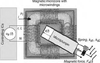
Figure 21.128 illustrates a microelectromechanical device (translational microtransducer) with a station-
ary member (magnetic core with windings) and movable member (microplunger), which can be fabri-
cated using the micromachining technology. Our goal is to perform the analysis and modeling of the
microtransducer developing the lamped-parameter mathematical model. That is, the goal is to derive
the differential equations which model the microtransducer steady-state and dynamic behavior.
FIGURE 21.128 Schematic of the translational microtransducer with controlling ICs.
9258_C021_Sect002-005.fm Page 102 Wednesday, October 10, 2007 7:10 PM
Actuators 21-103
Applying Newton’s second law for translational motion, we have
where x denotes the microplunger displacement, m is the mass of a movable member (microplunger),
B
v
is the viscous friction coefficient, k
s1
and k
s2
are the spring constants, and F
e
(t) is the magnetic force
It should be emphasized that the restoring/stretching force exerted by the spring is given by (k
s1
x + k
s2
x
2
).
Assuming that the magnetic system is linear, the coenergy is found to be W
c
(i, x) = L(x)i
2
and the
electromagnetic force developed is given by
In this formula, the analytic expression for the term dL(x)/dx must be found. The inductance is
where
ℜ
f
and
ℜ
g
are the reluctances of the magnetic material and air gap; A
f
and A
g
are the cross-sectional
areas; l
f
and (x + 2d) are the lengths of the magnetic material and the air gap.
Thus
Using Kirchhoff’s law, the voltage equation for the electric circuit is
where the flux linkage
ψ
is
ψ
= L(x)i.
Thus, one obtains
Therefore, the following nonlinear differential equation results:
Ft() m
d
2
x
dt
2
--------
B
v
dx
dt
------
k
s1
xk
s2
x
2
+()F
e
t()++ +=
F
e
i, x()
∂
W
c
i, x()
∂
x
----------------------
=
1
2
--
F
e
i, x()
1
2
--
i
2
dL x()
dx
--------------
=
Lx()
N
2
ℜ
f
ℜ
g
+
------------------
N
2
µ
f
µ
0
A
f
A
g
A
g
l
f
2A
f
µ
f
x 2d+()+
-------------------------------------------------
==
dL
dx
------
2N
2
µ
f
2
µ
0
A
f
2
A
g
A
g
l
f
2A
f
µ
f
x 2d+()+[]
2
--------------------------------------------------------–=
u
a
ri
d
ψ
dt
-------
+=
u
a
ri L x()
di
dt
-----
i
dL x()
dx
--------------
dx
dt
------
++=
di
dt
-----
r
Lx()
-----------
i–
2N
2
µ
f
2
µ
0
A
f
2
A
g
Lx()A
g
l
f
2A
f
µ
f
x 2d+()+[]
2
-------------------------------------------------------------------
iv
1
Lx()
-----------
µ
a
++=
9258_C021_Sect002-005.fm Page 103 Wednesday, October 10, 2007 7:10 PM
21-104 Mechatronic Systems, Sensors, and Actuators
Augmenting this equation with the differential equation and the torsional-mechanical dynamics
three nonlinear differential equations for the considered translational microtransducer are found to be
The derived differential equations represent the lumped-parameter mathematical model of the
microtransducer. Although, in general, the high-fidelity modeling must be performed integrating nonlin-
earities (for example, nonlinear magnetic characteristics and hysteresis) and secondary effects, the
lumped-parameter mathematical models as given in the form of nonlinear differential equations have
been validated for microtransducers. It is found that the major phenomena and effects are modeled for
the current, velocity, and displacement (secondary effects such as Coulomb friction, hysteresis and eddy
currents, fringing effect and other phenomena have not been modeled and analyzed). However, the
lumped-parameter modeling provides one with the capabilities to attain reliable preliminary steady-state
and dynamic analysis using primary circuitry and mechanical variables. It is also important to emphasize
that the voltage, applied to the microwinding, is regulated by ICs. The majority of ICs to control
microtransducers are designed using the pulse-width-modulation topologies. The switching frequency
of ICs is usually 1 MHz or higher. Therefore, as was shown, it is very important to study the microtrans-
ducer performance at the high operating frequency. This can be performed using Maxwell’s equations,
which will lead to the high-fidelity mathematical models [2].
21.5.4 Single-Phase Reluctance Micromotors: Microfabrication,
Modeling, and Analysis
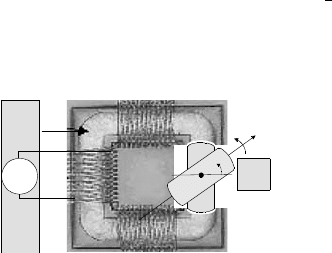
Consider the single-phase reluctance micromachined motors as illustrated in Figure 21.129.
The emphases are concentrated on the analysis, modeling, and control of reluctance micromotors in
the rotational microtransducer applications. Therefore, mathematical models must be found. The
lumped-parameter modeling paradigm is based upon the use of the circuitry (voltage and current) and
mechanical (velocity and displacement) variables to derive the differential equations using Newton’s and
Kirchhoff’s laws. In these differential equations, the micromotor parameters are used. In particular, for
the studied micromotor, the parameters are the stator resistance r
s
, the magnetizing inductances in the
quadrature and direct axes L
mq
and L
md
, the average magnetizing inductance , the leakage inductance
L
ls
, the moment of inertia J, and the viscous friction coefficient B
m
.
FIGURE 21.129 Single-phase reluctance micromotor with ICs and rotor displacement (position) sensor.
Ft() m
d
2
x
dt
2
--------
= B
v
dx
dt
------
k
s1
xk
s2
x
2
+()F
e
t()++ +
di
dt
-----
rA
g
l
f
2A
f
µ
f
x 2d+()+[]
N
2
µ
f
µ
0
A
f
A
g
--------------------------------------------------------
i–
2
µ
f
A
f
A
g
l
f
2A
f
µ
f
x 2d+()+
-------------------------------------------------
iv
A
g
l
f
2A
f
µ
f
x 2d+()+
N
2
µ
f
µ
0
A
f
A
g
-------------------------------------------------
u
a
++=
dv
dt
-----
N
2
µ
f
2
µ
0
A
f
2
A
g
mA
g
l
f
2A
f
µ
f
x 2d+()+[]
2
-------------------------------------------------------------
i
2
1
m
----
k
s1
xk
s2
x
2
+()–
B
v
m
-----
v–=
dx
dt
------
v=
L
m
Stator
u
as
(t)
r
s
, L
s
N
s
i
as
ICs
Rotor
ω
r,
T
e
r
θ
Sensor
θ
r
9258_C021_Sect002-005.fm Page 104 Wednesday, October 10, 2007 7:10 PM

Actuators 21-105
The expression for the electromagnetic torque was derived in [8]. In particular,
where L
∆m
is the half-magnitude of the sinusoidal magnetizing inductance L
m
variations,
Thus, to develop the electromagnetic torque, the current i
as
must be fed as a function of the rotor
angular displacement
θ
r
. For example, if i
as
= i
M
Re( ), then
The micromotor under our consideration is the synchronous micromachine, and the obtained expres-
sion for the phase current is very important to control the microtransducer. In particular, the Hall-effect
position sensor should be used to measure the rotor displacement, and the ICs must feed the phase
current as a nonlinear function of
θ
r
. Furthermore, the electromagnetic torque is controlled by changing
the current magnitude i
M
.
The mathematical model of the single-phase reluctance micromotor is found using Kirchhoff’s and
Newton’s second laws. In particular, we have
(circuitry equation—Kirchhoff ’s law)
(torsional–mechanical equation—Newton’s law)
Here, the electrical angular velocity
ω
r
and displacement
θ
r
are used as the mechanical system variables.
From u
as
= r
s
i
as
+ and the flux linkage equation
ψ
as
= (L
ls
+ − L
∆m
cos2
θ
r
)
as
, using the torsional-
mechanical dynamics, one obtains a set of three first-order nonlinear differential equations which models
single-phase reluctance micromotors. In particular, we have
As the mathematical model is found and the micromotor parameters are measured, nonlinear simu-
lation and analysis can be straightforwardly performed to study the dynamic responses and analyze the
micromotor efficiency. In particular, the resistance, inductances, moment of inertia, viscous friction
coefficient, and other parameters can be directly measured or identified based upon micromotor testing.
The steady-state and dynamic analysis based upon the lumped-parameter mathematical model is straight-
forward. However, the lumped-parameter mathematical models simplify the analysis, and thus, these
models must be compared with the experimental data to validate the results.
The disadvantage of single-phase reluctance micromotors are high torque ripple, vibration, noise, low
reliability, etc. Therefore, let us study three-phase synchronous reluctance micromotors.
T
e
L
∆m
i
as
2
2
θ
r
sin=
L
m
θ
r
() L
m
L
∆m
2
θ
r
cos–=
2
θ
r
sin
T
eaverage
1
π
---
L
∆m
i
as
2
2
θ
r
θ
r
dsin
0
π
1
4
--
L
∆m
i
M
2
==
u
as
r
s
i
as
d
ψ
as
dt
----------
+=
T
e
B
m
ω
r
– T
L
– J
d
2
θ
r
dt
2
----------
=
d
ψ
as
dt
---- ---- --
L
m
di
as
dt
--------
r
s
L
ls
L
m
L
∆m
2
θ
r
cos–+
--------------------------------------------------
i
as
2L
∆m
L
ls
L
m
L
∆m
2
θ
r
cos–+
--------------------------------------------------
i
as
ω
r
2
θ
r
1
L
ls
L
m
L
∆m
2
θ
r
cos–+
--------------------------------------------------
u
as
+sin––=
d
ω
r
dt
---------
1
J
--
L
∆m
i
as
2
2
θ
r
B
m
ω
r
– T
L
–sin()=
d
θ
r
dt
--------
ω
r
=
9258_C021_Sect002-005.fm Page 105 Wednesday, October 10, 2007 7:10 PM
21-106 Mechatronic Systems, Sensors, and Actuators
21.5.5 Three-Phase Synchronous Reluctance Micromotors: Modeling and
Analysis
Our goal is to address and solve a spectrum of problems in analysis, modeling, and control of synchronous
reluctance micromachines. The electromagnetic features must be thoroughly analyzed before attempt to
control micromotors. In fact, electromagnetic features significantly restrict the control algorithms to be
applied. Depending upon the conceptual methods employed to analyze synchronous reluctance micro-
machines, different control laws can be designed and implemented using ICs. Analysis and control of
synchronous reluctance micromotors can be performed using different modeling, analysis, and optimi-
zation concepts. Complete lumped-parameter mathematical models of synchronous reluctance micro-
motors in the machine (abc) and in the quadrature, direct, and zero (qd0) variables should be developed
in the form of nonlinear differential equations. In particular, the circuitry lumped-parameters mathe-
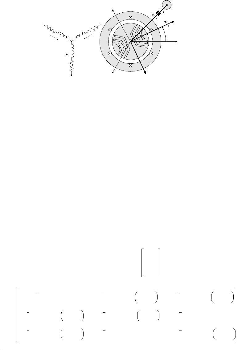
matical model is found using the Kirchhoff’s voltage law. We have, see Figure 21.130,
where u
as
, u
bs
, and u
cs
are the phase voltages; i
as
, i
bs
, and i
cs
are the phase currents;
ψ
as
,
ψ
bs
, and
ψ
cs
are the
flux linkages,
FIGURE 21.130 Three-phase synchronous reluctance micromotor.
Direct magnetic axis
as magnetic axis
Quadrature magnetic axi
s
bs
as′
bs magnetic axis
cs
bs′
cs magnetic axis
as
cs′
0
)(
θ
ττ
θ
+=
∫
t
t
0
d
Rotor
r
T
e
T
L
B
m
Load
Stator
+
L
ss
r
s
u
as
i
as
N
s
+
L
ss
r
s
u
bs
i
bs
+
L
ss
r
s
i
cs
u
cs
ω
ω
ω
u
abcs
r
s
i
abcs
=
d
ψ
abcs
dt
--------------
+
ψ
abcs
L
s
i
abcs
, r
s
r
s
00
0 r
s
0
00r
s
==
L
s
L
ls
L
m
L
∆m
2
θ
r
()cos–+
1
2
--
L
m
– L
∆m
2
θ
r
1
3
--
π
–cos–
1
2
--
L
m
– L
∆m
2
θ
r
1
3
--
π
+cos–
1
2
--
L
m
– L
∆m
2
θ
r
1
3
--
π
–cos– L
ls
L
m
L
∆m
2
θ
r
2
3
--
π
–cos–+
1
2
--
L
m
– L
∆m
2
θ
r
π
+()cos–
1
2
--
L
m
– L
∆m
2
θ
r
1
3
--
π
+cos–
1
2
--
L
m
– L
∆m
2
θ
r
π
+()cos– L
ls
L
m
L
∆m
2
θ
r
2
3
--
π
+cos–+
=
L
m
1
3
--
L
mq
L
md
+()and L
∆m
1
3
--
L
md
L
mq
–()==
9258_C021_Sect002-005.fm Page 106 Wednesday, October 10, 2007 7:10 PM
Actuators 21-107
The micromachine parameters are the stator resistance r
s
, the magnetizing inductances in the quadra-
ture and direct axes L
mq
and L
md
, the average magnetizing inductance , the leakage inductance L
ls
, the
moment of inertia J, and the viscous friction coefficient B
m
.
The expressions for inductances are nonlinear functions of the electrical angular displacement
θ
r
.
Hence, the torsional–mechanical dynamics must be used. Taking note of the Newton’s second law of
rotational motion, and using
ω
r
and
θ
r
(electrical angular velocity and displacement) as the state variables
(mechanical variables), one obtains
where T
e
and T
L
are the electromagnetic and load torques.
Torque Production Analysis—Using the coenergy, the electromagnetic torque, which is a nonlinear
function of the micromotor variables (phase currents and electrical angular position) and micromotor
parameters (number of poles P and inductance L
∆m
), is found to be [8],
To control the angular velocity, the electromagnetic torque must be regulated. To maximize the
electromagnetic torque, ICs must feed the following phase currents as functions of the angular displace-
ment measuring or observing (sensorless control)
θ
r
Thus, for
ϕ
i
= 0.3245, one obtains
That is, T
e
is maximized and controlled by changing the magnitude of the phase currents i
M
. Furthermore,
it is no torque ripple (in practice, based upon the experimental results, and performing the high-fidelity
modeling integrating nonlinear electromagnetics using Maxwell’s equations, one finds that there exists
the torque ripple which is due to the cogging torque, eccentricity, bearing, pulse-width-modulation, and
other phenomena).
The majority of ICs are designed to control the phase voltages u
as
, u
bs
, and u
cs
. Therefore, the three-
phase balance voltage set is important. We have
where u
M
is the magnitude of the supplied voltages.
L
m
T
e
B
m
2
P
---
ω
r
– T
L
– J
2
P
---
d
ω
r
dt
---------
,
d
θ
r
dt
--------
ω
r
==
T
e
P
2
---
L
∆m
i
as
2
2
θ
r
2i
as
i
bs
2
θ
r
1
3
--
π
– 2i
as
i
cs
2
θ
r
1
3
--
π
+sin+sin+sin=
i
bs
2
2
θ
r
2
3
--
π
– 2i
bs
i
cs
2
θ
r
i
cs
2
2
θ
r
2
3
--
π
+sin+sin+sin+
i
as
2i
M
θ
r
1
3
--
ϕ
i
π
+sin=
i
bs
2i
M
θ
r
1
3
--
2
ϕ
i
–()
π
–sin=
i
cs
2i
M
θ
r
1
3
--
2
ϕ
i
+()
π
+sin=
T
e
2PL
∆m
i
M
2
=
u
as
2u
M
θ
r
1
3
--
ϕ
i
π
+sin=
u
bs
2u
M
θ
r
1
3
--
2
ϕ
i
–()
π
–sin=
u
cs
2u
M
θ
r
1
3
--
2
ϕ
i
+()
π
+sin=
9258_C021_Sect002-005.fm Page 107 Wednesday, October 10, 2007 7:10 PM

21-108 Mechatronic Systems, Sensors, and Actuators
The mathematical model of synchronous reluctance micromotors in the abc variables is found to be
di
as
dt
--------
1
L
D
-----
r
s
i
as
u
as
–()4L
ls
2
3L
m
2
3L
∆m
2
– 8L
m
L
ls
4L
ls
L
∆m
2
θ
r
cos–++()
=
r
s
i
bs
u
bs
–()3L
m
2
3L
∆m
2
– 2L
m
L
ls
4L
ls
L
∆m
2
θ
r
1
3
--
π
–cos+++
r
s
i
cs
u
cs
–()3L
m
2
3L
∆m
2
– 2L
m
L
ls
4L
ls
L
∆m
2
θ
r
1
3
--
π
+cos+++
63L
∆m
2
L
ls
ω
r
i
cs
i
bs
–()8L
∆m
L
ls
2
ω
r
12L
∆m
L
m
L
ls
ω
r
+()++
2
θ
r
i
as
2
θ
r
1
3
--
π
– i
bs
2
θ
r
1
3
--
π
+ i
cs
sin+sin+sin×
di
bs
dt
--------
1
L
D
-----
r
s
i
as
u
as
–()3L
m
2
3L
∆m
2
– 2L
m
L
ls
4L
ls
L
∆m
2
θ
r
1
3
--
π
–cos++
=
r
s
i
bs
u
bs
–()4L
ls
2
3L
m
2
3L
∆m
2
– 8L
m
L
ls
4L
ls
L
∆m
2
θ
r
1
3
--
π
+cos–+++
r
s
i
cs
u
cs
–()3L
m
2
3L
∆m
2
– 2L
m
L
ls
4L
ls
L
∆m
2
θ
r
cos++[]+
63L
∆m
2
L
ls
ω
r
i
as
i
cs
–()8L
∆m
L
ls
2
ω
r
12L
∆m
L
m
L
ls
ω
r
+()++
2
θ
r
1
3
--
π
– i
as
2
θ
r
1
3
--
π
+ i
bs
2
θ
r
i
cs
sin+sin+sin×
di
cs
dt
--------
1
L
D
-----
r
s
i
as
u
as
–()3L
m
2
3L
∆m
2
– 2L
m
L
ls
4L
ls
L
∆m
2
θ
r
1
3
--
π
+cos++
=
r
s
i
bs
u
bs
–()3L
m
2
3L
∆m
2
– 2L
m
L
ls
4L
ls
L
∆m
2
θ
r
cos++()+
r
s
i
cs
u
cs
–()4L
ls
2
3L
m
2
3L
∆m
2
– 8L
m
L
ls
4L
ls
L
∆m
2
θ
r
1
3
--
π
–cos–+++
63L
∆m
2
L
ls
ω
r
i
bs
i
as
–()8L
∆m
L
ls
2
ω
r
12L
∆m
L
m
L
ls
ω
r
+()++
2
θ
r
1
3
--
π
+ i
as
2
θ
r
i
bs
2
θ
r
1
3
--
π
– i
cs
sin+sin+sin×
d
ω
r
dt
---------
P
2
4J
-----
L
∆m
i
as
2
2
θ
r
2i
as
i
bs
2
θ
r
1
3
--
π
– 2i
as
i
cs
2
θ
r
1
3
--
π
+sin+sin+sin=
i
bs
2
2
θ
r
2
3
--
π
– 2i
bs
i
cs
2
θ
r
i
cs
2
2
θ
r
2
3
--
π
+
B
m
J
------
ω
r
–
P
2J
-----
T
L
–sin+sin+sin+
d
θ
r
dt
--------
ω
r
=
9258_C021_Sect002-005.fm Page 108 Wednesday, October 10, 2007 7:10 PM
Actuators 21-109
Here
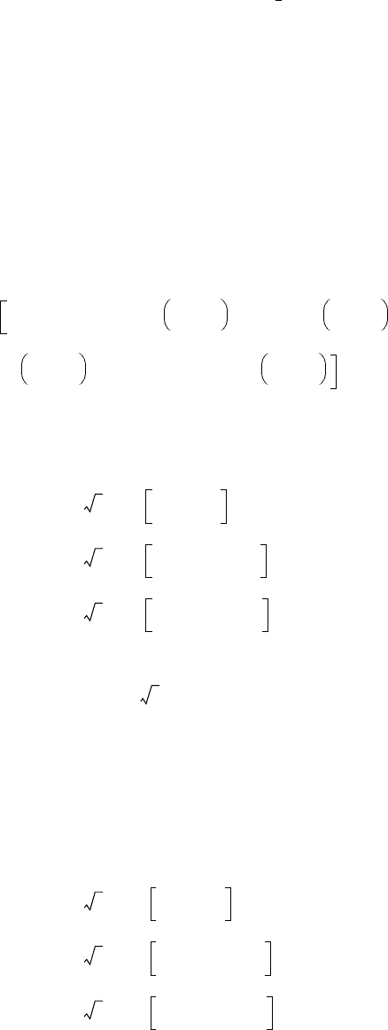
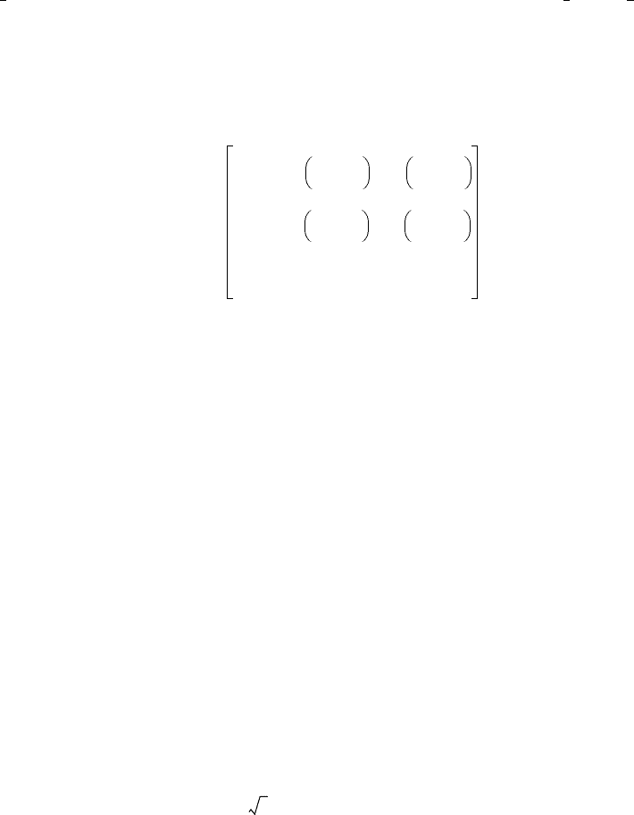
The mathematical model can be simplified. In particular, in the rotor reference frame, we apply the
Park transformation [8]
where u
qs
, u
ds
, u
0s
, i
qs
, i
ds
, i
0s
, and
ψ
qs
,
ψ
ds
,
ψ
0s
are the qd0 voltages, currents, and flux linkages.
Using the circuitry and torsional–mechanical dynamics, one finds the following nonlinear differential
equations to model synchronous reluctance micromotors in the rotor reference frame:
One can easily observe that this model is much simpler compared with the lumped-parameter math-
ematical model derived using the abc variables.
To attain the balanced operation, the quadrature and direct currents and voltages must be derived
using the direct Park transformation = , = . Hence, the qd0 voltages , ,
and are found using the three-phase balance voltage set. In particular, we have
We derived the mathematical models of three-phase synchronous reluctance micromotors. Based upon
the differential equations obtained, nonlinear analysis can be performed, and the phase currents and
voltages needed to guarantee the balance operating conditions can be found. The results reported can
be straightforwardly used in nonlinear simulation.
21.5.6 Microfabrication Aspects
The fabrication of electromechanical microstructures and microtransducers can be made through dep-
osition of the conductors (coils and windings), magnetic core, insulating layers, as well as other micro-
structures (movable and stationary members and their components). The order of the processes,
L
m
1
3
--
L
mq
L
md
+(), L
∆m
1
3
--
L
md
L
mq
–()and L
D
L
ls
9L
∆m
2
4L
ls
2
12L
m
L
ls
9L
m
2
–––()== =
u
qd0s
r
K
s
r
u
abcs
, i
qd0s
r
K
s
r
i
abcs
,
ψ
qd0s
r
K
s
r
ψ
abcs
== =
K
s
r
2
3
--
θ
r
cos
θ
r
2
3
--
π
–cos
θ
r
2
3
--
π
+cos
θ
r
sin
θ
r
2
3
--
π
–sin
θ
r
2
3
--
π
+sin
1
2
--
1
2
--
1
2
--
=
di
qs
r
dt
--------
r
s
L
ls
L
mq
+
--------------------
i
qs
r
L
ls
L
md
+
L
ls
L
mq
+
--------------------
i
ds
r
ω
r
–
1
L
ls
L
mq
+
--------------------
u
qs
r
+–=
di
ds
r
dt
--------
r
s
L
ls
L
md
+
--------------------
i
ds
r
L
ls
L
mq
+
L
ls
L
md
+
--------------------
i
qs
r
ω
r
1
L
ls
L
md
+
--------------------
u
ds
r
++–=
di
0s
r
dt
--------
r
s
L
ls
-----
i
0s
r
1
L
ls
-----
u
0s
r
+–=
d
ω
r
dt
---------
3P
2
8J
--------
L
md
L
mq
–()i
qs
r
i
ds
r
B
m
J
------
ω
r
–
P
2J
-----
T
L
–=
d
θ
r
dt
--------
ω
r
=
i
qd0 s
r
K
s
r
i
abcs
u
qd0s
r
K
s
r
u
abcs
u
qs
r
u
ds
r
u
0s
r
u
qs
r
2u
M
, u
ds
r
0, u
0s
r
0===
9258_C021_Sect002-005.fm Page 109 Wednesday, October 10, 2007 7:10 PM
21-110 Mechatronic Systems, Sensors, and Actuators
materials, and sequential steps are different depending on the MEMS which must be devised, designed,
analyzed, and optimized first.
21.5.6.1 Conductor Thin Films Electrodeposition
The conductors (microcoils to make windings) in microstructures and microtransducers can be fabricated
by electrodepositing the copper and other low resistivity metals. Electrodeposition of metals is made by
immersing a conductive surface in a solution containing ions of the metal to be deposited. The surface
is electrically connected to an external power supply, and current is fed through the surface into the
solution. In general, the reaction of the metal ions (Metal
x+
) with x electrons (xe
−
) to form metal (Metal)
is Metal
x+
+ xe
−
= Metal.
To electrodeposit copper on the silicon wafer, the wafer is typically coated with a thin conductive
layer of copper (seed layer) and immersed in a solution containing cupric ions. Electrical contact is
made to the seed layer, and current is flowed (passed) such that the reaction Cu
2+
+ 2e
−
→ Cu occurs at
the wafer surface. The wafer, which is electrically interacted such that the metal ions are changed to
metal atoms, is the cathode. Another electrically active surface (anode) is the conductive solution to
make the electrical path. At the anode, the oxidation reaction occurs that balances the current flow at
the cathode, thus maintaining the electric neutrality. In the case of copper electroplating, all cupric ions
removed from solution at the wafer cathode are replaced by dissolution from the copper anode.
According to the Faraday law of electrolysis, in the absence of secondary reactions, the current delivered
to a conductive surface during electroplating is proportional to the quantity of the metal deposited.
Thus, the metal deposited can be controlled varying the electroplating current (current density) and
the electrodeposition time.
The hydrated Cu ions reaction is
and the cathode reactions are
The copper electroplating solution commonly used is CuSO
4
–5H
2
O (250 g/l) and H
2
SO
4
(25 ml/l).
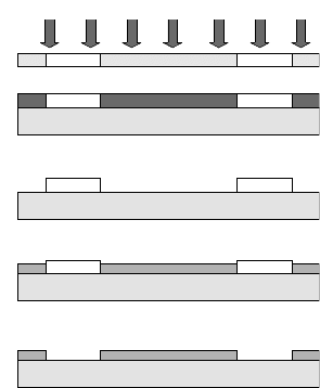
The basic processes are shown in Figure 21.131, and the brief description of the sequential steps and
equipment that can be used are given.
It must be emphasized that commonly used magnetic materials and conductors do not adhere well to
silicon. Therefore, as was described, the adhesion layers (e.g., titanium Ti or chromium Cr) are deposited
on the silicon surface prior to the magnetic material electroplating.
The electrodeposition rate is proportional to the current density and, therefore, the uniform current
density at the substrate seed layer is needed to attain the uniform thickness of the electrodeposit. To
achieve the selective electrodeposition, portions of the seed layer are covered with the resist (the current
density at the mask edges nonuniform degrading electroplating). In addition to the current density, the
deposition rate is also a nonlinear function of temperature, solution (chemicals), pH, direct/reverse
current or voltage waveforms magnitude, waveform pulses, duty ratio, plating area, etc. In the simplest
form, the thickness and electrodeposition time for the specified materials are calculated as
Cu
++
Cu H
2
O()
6
++
→
Cu
++
2e
−
Cu, Cu
++
e
−
Cu
+
,Cu
+
e
−
Cu, 2Cu
+
Cu
++
Cu, H
+
e
−
1
2
--
H
2
→++→→+→+→+
Thickness
material
Time
electroplating
Current
density
× Weight
molecular
×
Faraday
constant
Density
material
× Electron
number
×
------------------------------------------------------------------------------------------------------------
=
Time
electroplating
Thickness
material
Faraday
constant
× Density
material
Electron
number
××
Current
density
Weight
molecular
×
------------------------------------------------------------------------------------------------------------------------------------------------------
=
9258_C021_Sect002-005.fm Page 110 Wednesday, October 10, 2007 7:10 PM
Actuators 21-111
It was emphasized that electroplating is used to deposit thin-film conductors and magnetic materials.
However, microtransducers need the insulation layers, otherwise the magnetic core and coils as well as
multilayer microcoils themself will be short-circuited. Furthermore, the seed layers are embedded in
microfabrication processes. As the magnetic core is fabricated on top of the microcoils (or microcoils
are made on the magnetic core), the seed layer is difficult to remove because it is at the bottom or at the
center of the microstructure. The mesh seed layer can serve as the electroplating seed layer for the lower
conductors, and as the microstructure is made, the edges of the mesh seed layer can be exposed and
removed through plasma etching [6]. Thus, the microcoils are insulated. It should be emphasized that
relatively high aspect ratio techniques must be used to fabricate the magnetic core and microcoils, and
patterning as well as surface planarization issues must be addressed.
21.5.6.2 NiFe Thin Films Electrodeposition
Magnetic cores in microstructures and microtransducers must be made. For example, the electroplated
Ni
x%
Fe
100−x%
thin films, such as permalloy Ni
80%
Fe
20%
, can be deposited to form the magnetic core of
microtransducers (actuators and sensors), inductors, transformers, switches, etc. The basic processes and
sequential steps used are similar to the processes for the copper electrodeposition and the electroplating
is done in the electroplating bath. The windings (microcoils) must be insulated from magnetic cores,
and therefore, the insulation layers must be deposited. The insulating materials used to insulate the
windings from the magnetic core are benzocyclobutene, polyimide (PI-2611), etc. For example, the cyclo-
tene 7200-35 is photosensitive and can be patterned through photolithography. The benzocyclobutene,
FIGURE 21.131 Electrodeposition of copper and basic processes: silicon, kapton, and other substrates, can be used.
After clearing, the silicon substrate is covered with a 5–10 nm chromium or titanium and 100–200 nm copper seed
layer by sputtering. The copper microcoils (microstructures) are patterned using the UV photolitography. The AZ-
4562 photoresist can be spincoated and prebaked on a ramped hot plate at 90–100°C (ramp 30–40% with initial
temperature 20–25°C) for one hour. Then, the photoresist is exposed in the Karl Suss Contact Masker with the energy
1200–1800 mJ cm
2
. The development is released in 1:4 diluted alkaline solution (AZ-400) for 4–6 min. This gives
the photoresist thickness 15–25
µ
m. Copper is electroplated with a three-electrode system with a copper anode and
a saturated calomel reference electrode (the current power supply is the Perkin Elmer Current Source EG&G 263).
The Shipley sulfate bath with the 5–10 ml/l brightener to smooth the deposit can be used. The electrodeposition is
performed at 20–25°C with magnetic stirring and the dc current density 40–60 mA/cm
2
(this current density leads
to smooth copper thin films with the 5–10 nm rms roughness for the 10
µ
m thickness of the deposited copper thin
film). The resistivity of the electrodeposited copper thin film (microcoils) is 1.6–1.8
µ
Ω cm (close to the bulk copper
resistivity). After the deposition, the photoresist is removed.
1
Silicon substrate
2 Development
Photolithography mask
Photoresist
UV light
Silicon substrate
3 Copper electrodeposition
Silicon substrate
Electrodeposited Cu
4 Removal and etching
Silicon substrate
Electrodeposited Cu
9258_C021_Sect002-005.fm Page 111 Wednesday, October 10, 2007 7:10 PM
