Bichop R.H. (Ed.) Mechatronic Systems, Sensors, and Actuators: Fundamentals and Modeling
Подождите немного. Документ загружается.

21-22 Mechatronic Systems, Sensors, and Actuators
In summary, when the transistor is saturated, it acts as a closed switch. When a transistor is in the cutoff
region, it acts as an open switch. When it is in the active region, it acts as a current (i
B
) controlled current
(i
C
) amplifier. Although this is a very simplistic approximation, it is very useful for designing and
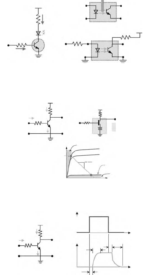
understanding power electronics and interfacing electromechanical systems. Figure 21.35 illustrates some
examples of BJT devices and applications.
When carefully controlling the base-emitter voltage
V
BE
and base current
i
B
, the transistor can be made
to operate between the cutoff and the saturation region, which act as a switch, see Figure 21.36. Realistically,
transistor switching is not instantaneous (see Figure 21.37). The turn-on time
t
ON
of the transistor is the
FIGURE 21.35 Some examples of using BJT.
FIGURE 21.36 BJT as a current controlled switch.
FIGURE 21.37 BJT switching characteristics.
Photo-intrerrupter
Opto-isolator
V
IN
V
CC
I
B
I
C
V
IN
R
IN
R
B
LED
–
–
+
+
R
C
R
C
V
V
OUT
V
OUT
Using BJT as a switch to turn
off/off a LED
R
L
1
A
–
–
–
–
–
+
+
+
+
+
B
V
IN
i
B1
i
C
i
E
i
B
i
B
i
C
R
L
R
L
R
B
R
B
V
IN
V
OUT
V
CC
V
CC
V
CE
V
OUT
V
CE(SAT)
Cutoff
Saturation
0
∪
t
F
t
t
i
C
V
IN
R
L
V
IN
i
E
R
B
i
B
i
C
t
R
t
S
t
D
V
CC
V
OUT
ON
––
+
+
OFFOFF
9258_C021_Sect001.fm Page 22 Wednesday, October 10, 2007 7:09 PM
Actuators 21-23
sum of the delay time
t
D
and the rise time
t
R
. Similarly, the turn-off time
t
OFF
is the sum of the storage
time
t
S
and the fall time
t
F
. The turn-on and turn-off time of a transistor limits the maximum switching
frequency. Typical switching frequency for a power BJT is between 2 and 20 kHz. Generally speaking, BJTs
can switch at a higher frequency than thyristors but can handle less power. Power BJTs can handle currents
up to several hundred amperes and
V
CE
up to about 1 kV.
Power dissipation is a key design constraint for BJTs. Recall that if the BJT is used in the active linear
region (linear amplifier), the power dissipation is P
BJT
= i
C
· V
CE
with V
CE
> V
γ
. With a large collector
current and considering the small volume and thermal mass of the device, the transistor is not very efficient
when operating in the active linear region. On the other hand, when the BJT is switching between saturation
and cutoff, the collector current will be small (during cutoff) and V
CE
will be small (during saturation).
The switching power dissipation is much smaller compared with the active linear mode of operation. This
makes switching much more efficient.
One design consideration working with BJT is to supply adequate base current, especially when the
transistor is to operate in the saturated region, see Equation 21.13. This may require large input power
and may overload the input stage. As will be discussed later, this is also the main reason that BJTs are less
used in switching power electronics and are being replaced by devices such as MOSFET and IGBT, which
require much less control current. One solution to this constraint is to increase the current gain
β
. A
simple and elegant implementation to increase the effective current gain of a BJT is the Darlington pair
configuration.
Darlington Transistor Pairs
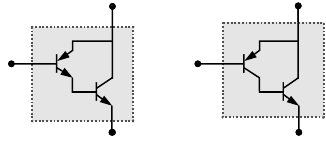
A Darlington transistor pair connects two BJT transistors to form an effective three terminal device that
has increased current gain, see Figure 21.38. In Figure 21.38, let
β
1
and
β
2
be the current gains of the
two transistors, then the relationship between the base current of transistor Q1 and the collector current
of transistor Q2 is
Therefore, the effective current gain for the Darlington transistor pair is the product of the two
individual current gains, i.e.,
β
D
=
β
1
·
β
2
. For a typical Darlington pair, this can be in the range of
500–10,000. The trade-off for using Darlington pair configuration is the additional space (real estate)
needed for two transistors instead of one.
Metal-Oxide-Semiconductor Field Effect Transistor (MOSFET)
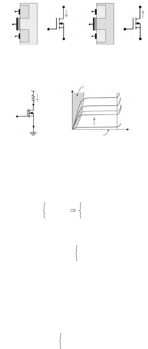
MOSFET is a type of field effect transistor (FET). FETs are voltage controlled three terminal devices respec-
tively called drain (D), source (S), and gate (G). The terms come from the analogy of overhead tank system
that uses a gate valve to control the water flow from source to drain. MOSFET uses a metal plate as the gate
terminal and it is insulated from the p- or n-type silicon substrate by a thin layer of oxide (see Figure 21.39).
When a gate voltage V
G
is applied to the gate plate, an electrostatic field induces reverse charges at the
gate and the substrate. The charges at the substrate initiate transistor type characteristics by forming either
an n-type channel or a p-type channel. Hence, the n- or p-type MOSFET classifications (see Figure 21.39).
FIGURE 21.38 Two type of Darlington transistor pairs.
Q1
Q2
bb
1
bb
2
C
E
Q1
Q2
1
2
B
β
β
C
E
i
C2
β
2
i
B2
⋅
β
2
β
1
i
B1
⋅()⋅
β
2
β
1
⋅()i
B1
⋅
β
D
i
B1
⋅== = =
9258_C021_Sect001.fm Page 23 Wednesday, October 10, 2007 7:09 PM
21-24 Mechatronic Systems, Sensors, and Actuators
For a majority of the power amplification and modulation applications, MOSFETs are designed to operate in
the enhancement mode. Figure 21.40 illustrates the enhancement mode characteristic of an n-channel MOSFET:
1. Cutoff—When the potential across the gate and the substrate (source) V
GS
is less that the turn-on
(threshold) voltage V
T
, the MOSFET is in the cutoff region and there is negligible current flow
through the drain (D) terminal, i.e.,
Typically, V
T
≈ 1–2 V. In this mode, the transistor from D to S can be viewed as an open connection.
2. Active Region—When the V
GS
> V
T
, the MOSFET is in the active region, where
In this mode, the transistor can be viewed as a voltage-controlled current amplifier, where the
drain current i
C
is proportional to square of the difference between the gate-source voltage and
the threshold voltage. The drain current is controlled by the gate-source voltage V
GS
. The power
dissipation across the transistor P
FET
is
P
FET
= i
D
· V
DS
3. Ohmic State—When V
GS
is large enough so that the drain current is determined by the drain
source circuit, the MOSFET is in saturation and
>> (21.14)
FIGURE 21.39 Metal-oxide-semiconductor (MOS) field effect transistor (FET).
FIGURE 21.40 Enhancement mode MOSFET characteristic.
Gate
Gate
p-channel MOSFETn-channel MOSFET
Source
Source
Drain
Drain
G
G
S
S
p
p
n
n
p
p
D
i
D
i
D
D
Ohmic state
constant current
Cutoff (V
GS
< V
T
)
Breakdown
BV
DS
V
DS
i
D
(mA)
–
–
+
+
S
G
D
i
D
R
D
V
DD
V
DS
V
GS
V
GS
Ψ
V
GS
V
T
<
i
G
0=
i
D
0≈
V
DS
V
DD
≈
V
GS
V
T
> and
i
D
V
GS
V
T
–()
2
∝
V
DS
V
GS
V
T
–>
V
GS
V
T
and
i
D
V
DD
/R
D
=
V
DS
i
D
R
ON
V
DS
()V
GS
V
T
–<⋅≈
9258_C021_Sect001.fm Page 24 Wednesday, October 10, 2007 7:09 PM
Actuators 21-25
In this mode, the transistor can be viewed as a closed switch between the terminals D and S with
a voltage controlled resistance R
ON
. The drain current i
D
is controlled (determined) by the drain
circuit. At rate current, the V
DS
drop during saturation ranges from 2 to 5 V.
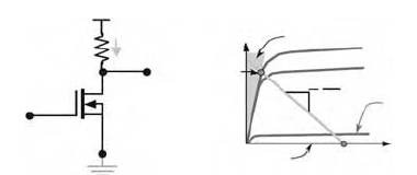
When operating in the enhancement mode, a MOSFET behaves very similar to a BJT. Instead of base
current, the MOSFET behavior is determined by the gate voltage. When carefully controlling the gate
voltage of a MOSFET, the transistor can be made to operate as a voltage controlled switch (Figure 21.41)
that operates between the cutoff (point A) and the Ohmic (point B) region.
One advantage of a MOSFET device is that the MOSFET has significantly larger input impedance as
compared to BJT. This simplifies the circuit that is needed to drive the MOSFET since the magnitude of
the gate current is not a factor. This also implies that a MOSFET is much more efficient than BJTs as
well as it can be switching at a much higher frequency. Typical MOSFET switching frequency is between
20 and 200 kHz, which is an order of magnitude higher than BJTs. Power MOSFETs can carry drain
currents up to several hundreds of amperes and V
DS
up to around 500 V.
Field effect is one of the key reasons why MOSFET has better switching performance than BJT.
However, static field is also one of its main failure modes. MOSFETs are very sensitive to static voltage.
Since the oxide insulating the gate and the substrate is only a thin film (in the order of a fraction to a
few micrometer), high static voltage can easily break down the oxide insulation. A typical gate breakdown
voltage is about 50 V. Therefore, static electricity control or insulation is very important when handling
MOSFET devices.
Comparing BJT with MOSFET, we can conclude the following:
•
Both can be used as current amplifiers.
•
BJT is a current-controlled amplifier where the collector current i
C
is proportional to the base
current i
B
.
•
MOSFET is a voltage-controlled amplifier where the drain current i
D
is proportional to the
square of the gate voltage V
G
.
•
Both can be used as three terminal switches or voltage inverters.
•
BJT: switching circuit give rise to TTL logics.
•
MOSFET: switching circuit give rise to CMOS logics.
•
BJT usually has larger current capacity than similar sized MOSFET.
•
MOSFET has much higher input impedance than BJT and is normally off, which translates to less
operating power.
•
MOSFETs are more easily fabricated into integrated circuit.
•
MOSFETs are less prone to go into thermal runaway.
•
MOSFETs are susceptible to static voltage (exceed gate breakdown voltage ∼50 V).
•
BJT has been replaced by MOSFET in low-voltage (<500 V) applications and is being replaced by
IGBT in applications at voltages above 500 V.
FIGURE 21.41 MOSFET as a voltage controlled switch.
V
DS
A
1
R
L
B
V
G1
V
IN
V
OUT
i
D
i
D
R
L
V
DD
D
G
S
+
–
–
+
Ohmic region
Cuttoff
9258_C021_Sect001.fm Page 25 Wednesday, October 10, 2007 7:09 PM
21-26 Mechatronic Systems, Sensors, and Actuators
Insulated Gate Bipolar Transistor (IGBT)
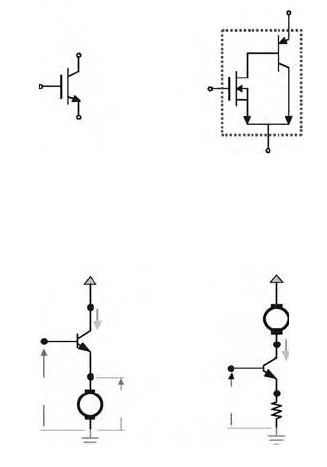
IGBT is a voltage-controlled transistor that has the terminals identified in the same way as BJTs. IGBT
is a four-layer device that has the similar construction of a MOSFET with an additional p layer.
Figure 21.42 shows the schematic symbol and equivalent circuit for an IGBT. IGBT has the combined
characteristics of the BJT and MOSFET. Similar to MOSFET, it has high input impedance and high
switching frequency. It also has high power handling capacity like the BJT.
21.1.3.5 Typical Power Amplifiers for Electromechanical Actuators
Power amplification and modulation for electromechanical actuators are classified into two basic cate-
gories, based on the methods the respective power electronics are driven. Linear amplifiers drive the BJTs
in their active linear region. Switching amplifiers drive the transistors in on-off switch mode. Depending
on the control objective, the command signal (Figure 21.2) to the amplifier can be either a voltage or
current command that intends to modulate the electric energy delivered to the energy conversion device.
Since most of the electromechanical actuator involves driving an inductance load such as a coil winding
of an electromagnet or the rotor of a DC motor, in the following discussion, we will use the DC motor
as an example of an inductance load for the power amplifier.
Linear Amplifiers
Figure 21.43 shows the basic drive circuit for linear voltage and current control amplifiers. Both schemes
have the following commonalities:
1. The input command voltage V
i
(t) is applied to the base of the transistor.
2. The electric power needed to driver the load is provided by a DC supply.
3. The transistors are driven in the active linear region.
Voltage Control (Mode) Amplifier
In Figure 21.43a, the motor is driven as a load of an emitter circuit. If the base-emitter voltage is ignored,
the voltage across the motor V
M
is directly controlled by the input voltage V
IN
and the current is supplied
by the power supply. The amount of current, on the other hand, depends on the applied voltage, speed,
and the motor parameter.
FIGURE 21.42 Insulated gate bipolar transistor (IGBT).
FIGURE 21.43 Two basic linear motor amplifiers.
B
E
C
B
E
Equivalent circuitSchematic symbol
C
V
IN
V
IN
V
IN
~
i
M
i
M
i
M
R
S
+V
+V
__
∼V
IN
(b) Current-mode driver(a) Volta
g
e-mode driver
∼
=
V
M
V
M
V
BE
–
~
V
IN
–V
BE
R
s
=
_______
V
IN
R
S
9258_C021_Sect001.fm Page 26 Wednesday, October 10, 2007 7:09 PM
Actuators 21-27
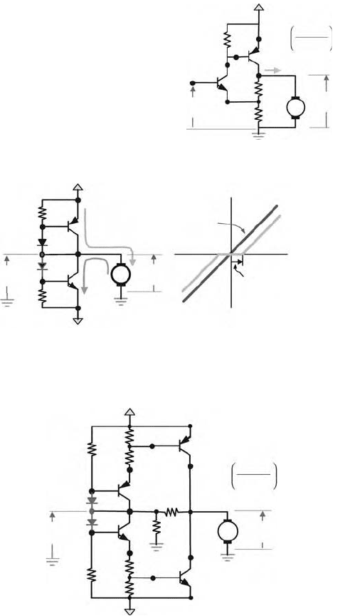
To provide adjustable voltage gain, Figure 21.44 shows a variable gain voltage-mode amplifier, where
the apparent amplifier gain from the command input V
IN
to the applied motor (winding) voltage V
M
can be approximated by (R
A
+ R
B
)/R
A
, which can be adjusted by proper selection of the resistors R
A
and
R
B
. If a large motor current is required, transistor Q2 can be replaced by a Darlington transistor pair.
The amplifiers shown in Figures 21.43 and 21.44 can only drive the current through the motor (load)
in one direction. Hence, they are also called unipolar amplifiers. To provide bidirectional current flow,
two transistors can be connected with the motor in a push-pull type configuration, as shown in
Figure 21.45. The two diodes in the circuit are used to eliminate the dead-zone created by the base-
emitter voltage drop for the transistors. Notice that a bipolar voltage source is needed for this configu-
ration. Figure 21.46 shows a bipolar voltage-mode driver with variable gain (R
A
+ R
B
)/R
A
. Similarly, if
larger motor current is required, transistors Q3 and Q4 can be replaced by Darlington transistor pairs.
FIGURE 21.44 Variable gain voltage-mode amplifier.
FIGURE 21.45 Bipolar voltage-mode amplifier.
FIGURE 21.46 Bipolar variable gain voltage-mode amplifier.
+V
Q2
Q1
V
M
≈
V
IN
V
IN
R
B
R
A
i
M
V
M
R
A
+ R
B
R
A
+V
With diode
Push
Pull
Approximately 0.6 V
dead-zone
–V
V
IN
V
IN
V
M
V
M
–V
+V
Q
2
Q
3
Q
4
Q
1
V
IN
R
B
R
A
V
M
≈
V
M
V
IN
R
a
+ R
b
R
a
9258_C021_Sect001.fm Page 27 Wednesday, October 10, 2007 7:09 PM
21-28 Mechatronic Systems, Sensors, and Actuators
Current Control (Mode) Amplifier
As previously discussed, in many electromagnetic actuators, the output force or torque of the device has
strong correlation with the winding current, e.g., for a permanent magnet DC motor and a voice coil
actuator, the output torque and force are proportional to the input current. Therefore, in many motion
control applications, it is more desirable to have a voltage-to-current conversion (current-mode amplifier)
at the power stage, where the input voltage command is proportional to the current flowing into/out of
the motor (winding). Figure 21.43b shows a basic circuit for a current-mode amplifier. The relationship
between the emitter (motor) current i
M
and the input voltage command V
IN
is
If the base-emitter voltage is ignored, the voltage across the motor current i
M
is proportional to the
input voltage V
IN
, i.e., i
M
≈ (1/R
S
) · V
IN
.
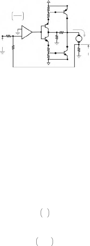
Figure 21.47 shows a basic bipolar current-mode amplifier. An Op-Amp is used to close the current
loop. The resistor R
S
, often called the sensing resistor, is used to sense the motor current for feedback to
the Op-Amp. Depending on the desired current magnitude, the sensing resistor needs to have adequate
power rating to dissipate the heat ( ) generated by flowing current through the resistor. For a zeroth
order approximation, at steady state, the Op-Amp will try to equalize the potential at the positive and
the negative terminals, i.e., it will try to make
,
which implies
.
Although a current amplifier tends to have a linear relationship between the command input and the
winding current, there is practical limitation due to the limited source voltage. In Figure 21.47, the supply
voltage is ±V. Assuming that the motor winding has resistance R
M
, the maximum current i
MAX
the voltage
source can supply is upper bounded by
.
FIGURE 21.47 Bipolar variable gain current-mode amplifier.
–V
+V
Q
3
Q
2
~
~
Q
4
Q
1
V
IN
R
B
R
1
R
A
V
S
R
A
R
2
R
2
R
S
i
M
i
M
.
V
IN
R
1
.
+
–
–
i
M
V
IN
V
BE
–
R
S
----------------------
=
i
M
2
R
S
⋅
V
S
−
R
2
R
1
-----
V
IN
⋅≈
i
M
−
R
2
R
S
R
1
⋅
---------------
V
IN
⋅≈
i
MAX
V
R
M
R
S
+
-------------------
<
9258_C021_Sect001.fm Page 28 Wednesday, October 10, 2007 7:09 PM
Actuators 21-29
The above bound has not considered the effect of the back-emf that will be induced in the winding
if the winding is moving. Hence, the amount of current available for a current-mode amplifier is limited
and needs to be considered when working with a current-mode amplifier.
Switching Amplifiers
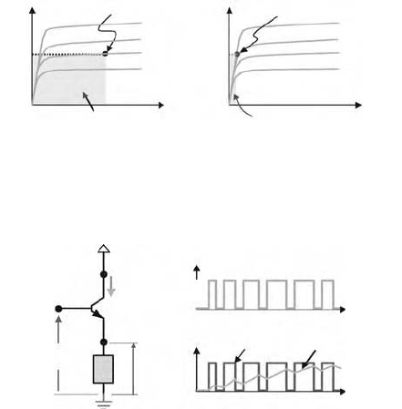
Linear amplifiers are simple and do not generate electrical noises. However, since the final stage transistors
are operating in the active linear region, significant power is dissipated into heat; this reduces the efficiency
of the device as well as requires large heat sinks to protect the components. However, as shown in
Figure 21.48, when operating in the saturation region, if the collector-emitter voltage drop is in the order
of 1 V or less, the power loss across the transistor is significantly less, given the same amount of current
flow. The trade-off is that additional circuits are needed to provide the modulation for current or voltage
control.
Figure 21.49 shows a simple switching amplifier that is simply a transistor connecting a load. It is
essentially the same as the basic linear amplifier shown in Figure 21.43a. The difference is in the way the
transistor is controlled. For a switching amplifier, the input (base) voltage only takes on two values (states),
high and low. When the base (input) voltage is high, the transistor is turned on in the saturation mode
and current will flow through the load. If we neglect the collector-emitter voltage drop, the voltage across
the load is approximately the supply voltage. When the base voltage is low, the transistor is turned off
in the cutoff state and no voltage is applied to the load. If the load has a low pass characteristic, the
average current/voltage across the load will be proportional to the turn-on time. Therefore, if the switching
frequency is sufficiently high (relative to the load impedance), the effective voltage/current across the
load can be modulated by the percent high input voltage, e.g., if the V
IN
is high 80% of the time, the
average voltage across the load will be close to 80% of the supplied voltage V. This is the so-called pulse-
width modulation (PWM). Another benefit of using switching amplifiers is that V
IN
can be directly interfaced
with a digital device without the need for a DAC.
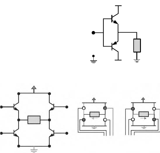
Push-Pull (Class B) Power Amplifier
The switching amplifier shown in Figure 21.49 is unipolar, i.e., it can only drive current through the load
in one direction. Figure 21.52 shows a simple
push-pull
(
Class B
) type power stage to supply bi-directional
current to the load. The circuit in Figure 21.50 is very similar to the bipolar voltage-mode amplifier shown
FIGURE 21.48 Power dissipation in transistors.
FIGURE 21.49 Simple switching amplifier with switching input.
Operating point
Operating point
Power dissipated
in the transistor
(b) Transistor in saturation region
(a) Transistor in active linear re
g
ion
Power dissipated
in the transistor
V
CE
i
C
i
C
V
CE
t
t
+V
V
IN
V
load
V
load
V
load
i
load
i
load
i
load
V
IN
9258_C021_Sect001.fm Page 29 Wednesday, October 10, 2007 7:09 PM
21-30 Mechatronic Systems, Sensors, and Actuators
in Figure 21.45. The difference is also in the way the transistors are controlled. When the base voltage
V
IN
is sufficiently positive (
+
V
), the push transistor Q
push
will be turned on and the pull transistor Q
pull
will
be turned off. This results in a load current flowing from positive supply to ground. If the base voltage is
sufficiently negative (
−
V
), Q
push
will be turned off and Q
pull
will be turned on, which results in a current
flow from ground to the negative supply. To modulate the load voltage/current, PWM can also be used.
This configuration is also called a
half H-bridge
driver or half-bridge driver for short. From an implemen-
tation perspective, this device requires both a positive supply and a negative supply, which tends to increase
the complexity and cost of the circuit.
H-Bridge Driver
H-bridge configuration is a neat solution to achieve bipolar operation with unipolar supply. Figure 21.51
shows a simple H-bridge circuit driving a load. An H-bridge consists of four transistors that are connected
in a Wheatstone bridge configuration. By turning on/off different pairs of transistors (Q1-Q3) or (Q2-Q4),
bipolar voltage across the load can be achieved using a unipolar supply, see Figure 21.51. In many
applications, the transistors pairs in the H-bridge can be directly driven by the output of a digital device
(TTL or CMOS). The n-p-n or n-channel transistors can be turn on to saturation by a high output from
the digital port and turned off by a low output. If large amount of current is required for the load,
Darlington pairs can be used in place of the individual transistors. Since MOSFETs have larger input
impedance and faster switching characteristics, they are replacing BJTs in almost all switching applications.
Pulse-Width Modulation (PWM)
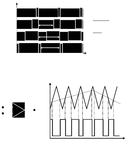
PWM is one of the more common ways of encoding analog information using digital signal. A PWM
signal is a wave of fixed frequency and varying duty cycle (pulse width). The duty cycle in PWM context
refers to the percentage of time that the signal is in the active state—usually this means a state of logic 1,
see Figure 21.52. In essence, PWM encodes (modulates) the information in the time domain rather than
the voltage domain as with analog signals.
PWM actuation has several advantages over the use of D/A converters and linear components. One
is the efficiency where the switching amplifiers are more efficient than their linear counter parts. Another
FIGURE 21.50 Switching push-pull amplifier.
FIGURE 21.51 H-bridge driver.
+V
V
IN
Load
Ð
v
+
−
Q
PUSH
Q
PULL
+V +V
+V
Q2
Q3Q4
HLHLLHLH
Load
Q1
i
load
i
load
++––
9258_C021_Sect001.fm Page 30 Wednesday, October 10, 2007 7:09 PM
Actuators 21-31
advantage is there is no need for D/A conversion. Digital signal is maintained from the microprocessor/
microcontroller to the power amplifier. In additional to having better noise rejection capability, this also
reduces the need for a DAC and tends to make the circuit simpler and more cost effective. One drawback
for using PWM and switching amplifiers as a whole is that the high frequency switching induces radio
frequency interference (RFI) and electromagnetic interference (EMI).
The fixed PWM carrier frequency is one main design consideration. Ideally, the PWM frequency should
be high enough to avoid generating audible switching noise, which mean that it should be greater than
20 kHz. However, there are a few factors that put an upper bound on the carrier frequency. Switching losses
of switching devices tends to increase as the switching frequency increases. This reduces the efficiency of
switching components and amplifiers. Higher PWM carrier frequency requires faster switching compo-
nents that cost more. The amount of current going through the device also limits the switching rate. In
general, sub-horsepower devices and office/desktop equipments usually use PWM at 20–40 kHz. For
larger scale industrial applications, the PWM frequency tends to be less than 500 Hz. Another commonly
specified design parameter is the PWM resolution. This is required for generating PWM from a digital
source. The PWM resolution is equivalent to the quantization resolution for ADC. An 8-bit PWM means
that there are 2
8
= 256 different pulse widths per PWM carrier signal period.
PWMs are widely adopted in the field and almost all microcontrollers and microprocessors have at
least one PWM output port. PWM signal can be easily generated from analog signal by comparing the
analog signal with a periodic triangular signal through a comparator, see Figure 21.53.
21.1.3.6 Interfacing Considerations
We will conclude this section by discussing some issues relating to interfacing between the electrome-
chanical actuator and the power amplification device.
Driving Inductive Load
A majority of the electromechanical actuators use coils (windings) to convert electrical energy to magnetic
energy. From a power driver viewpoint, windings are resistive and inductive loads. Inductors are energy
FIGURE 21.52 Pulse-width modulation signals.
FIGURE 21.53 Generating PWM signal from analog signal.
T
PWM
T
ON
T
OFF
10%
40%
70%
90%
Time
V
PWM
Duty cycle [%]
100%
T
ON
T
PWM
=
⋅
=
100%
T
ON
T
ON
+ T
OFF
⋅
+
Ð
>
V
TR
V
AN
V
PWM
Comparator
V
TR
V
AN
V
PWM
Time
+
Ð
>
+
Ð
>
9258_C021_Sect001.fm Page 31 Wednesday, October 10, 2007 7:09 PM
