Bhushan B. Handbook of Micro/Nano Tribology, Second Edition
Подождите немного. Документ загружается.


© 1999 by CRC Press LLC
Contributors
Phillip B. Abel, Ph.D.
NASA Lewis Research Center
Cleveland, Ohio
Alan Berman, Ph.D.
Tape Operations
Seagate Technology
Costa Mesa, California
Bharat Bhushan, Ph.D.
Department of Mechanical
Engineering
Ohio State University
Columbus, Ohio
Donald Brenner, Ph.D.
Department of Materials Science
and Engineering
North Carolina State University
Raleigh, North Carolina
Nancy A. Burnham, Ph.D.
Department of Physics
IGA – Ecole Polytechnique
Lausanne, Switzerland
Jaime Colchero, Ph.D.
Dep. Fisica de la Mat. Condensada
Universidad Autonoma de Madrid
Madrid, Spain
Fredric Ericson, Ph.D.
Department of Materials Science
Uppsala University
Uppsala, Sweden
John Ferrante, Ph.D.
Department of Physics
Cleveland State University
Cleveland, Ohio
Judith A. Harrison, Ph.D.
Chemistry Department
United States Naval Academy
Annapolis, Maryland
Jacob N. Israelachvili,
Ph.D.
Department of Chemical
Engineering
University of California
Santa Barbara, California
Hiroshi Kano, Ph.D.
Recording Media Division
Sony Corporation
Sakuragi Tagajo City, Japan
Hirofumi Kondo, Ph.D.
Recording Media Division
Sony Corporation
Sakuragi Tagajo City, Japan
Andrzej J. Kulik, Ph.D.
Department of Physics
IGA - Ecole Polytechnique
Lausanne, Switzerland
Othmar Marti, Ph.D.
Abteilung fuer Experimentelle
Physik
Universitaet Ulm
Ulm, Germany
Ernst Meyer, Ph.D.
Institut fur Physik
Basel, Switzerland
Richard S. Muller, Ph.D.
Berkeley Sensor & Actuator Center
University of California
Berkeley, California
Hiroyuki Osaki, Ph.D.
Recording Media Division
Sony Corporation
Sakuragi Tagajo City, Japan
Norio Saito, Ph.D.
Recording Media Division
Sony Corporation
Sakuragi Tagajo City, Japan
Jan-Åke Schweitz, Ph.D.
Department of Materials Science
Uppsala University
Uppsala, Sweden
Steven J. Stuart, Ph.D.
Chemistry Department
United States Naval Academy
Annapolis, Maryland
Hiroshi Takino, Ph.D.
Recording Media Division
Sony Corporation
Sakuragi Tagajo City, Japan

© 1999 by CRC Press LLC
Contents
Part I Basic Studies
1 Introduction—Measurement Techniques and Applications
Bharat Bhushan
2 AFM Instrumentation and Tips
Othmar Marti
3 Surface Physics in Tribology
John Ferrante and Phillip B. Abel
4 Characterization and Modeling of Surface Roughness and Contact Mechanics
Arun Majumdar and Bharat Bhushan
5 Surface Forces and Adhesion
Nancy Burnham and Adrzej A. Kulik
6 Friction on an Atomic Scale
Jaime Colchero, Ernst Meyer, and Othmar Marti
7 Microscratching/Microwear Nanofabrication/Nanomachining, and Nano/pico-
indentation Using Atomic Force Microscopy
Bharat Bhushan
8 Boundary Lubrication Studies Using Atomic Force/Friction Force
Microscopy
Bharat Bhushan
9 Surface Forces and Microrheology of Molecularly Thin Liquid Films
Alan Berman and Jacob N. Israelachvili
10 Nanomechanical Properties of Solid Surfaces and Thin Films
Bharat Bhushan
11 Atomic-Scale Simulations of Tribological and Related Phenomena
Judith A. Harrison, Steven J. Stuart, and Donald W. Brenner
Part II Applications
12 Design and Construction of Magnetic Storage Devices
Hirofumi Kondo,
Hiroshi Takino, Hiroyuki Osaki, Norio Saito, and Hiroshi Kano

© 1999 by CRC Press LLC
13 Microdynamic Systems in the Silicon Age
Richard S. Muller
14 Micro/Nanotribology and Micro/Nanomechanics of Magnetic Storage Devices
Bharat Bhushan
15 Mechanical Properties of Materials in Microstructure Technology
Fredric Ericson and Jan-Åke Schweitz
16 Micro/Nanotribology and Micro/Nanomechanics of MEMS Devices
Bharat Bhushan
Bhushan, B. “Introduction - Measurement Techniques and Applications”
Handbook of Micro/Nanotribology.
Ed. Bharat Bhushan
Boca Raton: CRC Press LLC, 1999

© 1999 by CRC Press LLC
Part I
Basic Studies

© 1999 by CRC Press LLC
1
Introduction —
Measurement
Techniques and
Applications
Bharat Bhushan
1.1 History of Tribology and Its Significance to Industry
1.2 Origins and Significance of Micro/Nanotribology
1.3 Measurement Techniques
Scanning Tunneling Microscope • Atomic Force Microscope •
Friction Force Microscope • Surface Force Apparatus •
Vibration Isolation
1.4 Magnetic Storage and MEMS Components
Magnetic Storage Devices • MEMS
1.5 Role of Micro/Nanotribology in Magnetic Storage
Devices, MEMS, and Other Microcomponents
References
In this chapter, we first present the history of macrotribology and micro/nanotribology and their indus-
trial significance. Next, we describe various measurement techniques used in micro/nanotribological
studies, then present the examples of magnetic storage devices and microelectromechanical systems
(MEMS) where micro/nanotribological tools and techniques are essential for interfacial studies. Finally,
we present examples of why micro/nanotribological studies are important in magnetic storage devices,
MEMS, and other microcomponents.
1.1 History of Tribology and Its Significance to Industry
Tribology is the science and technology of two interacting surfaces in relative motion and of related
subjects and practices. The popular equivalent is friction, wear, and lubrication. The word
tribology
,
coined in 1966, is derived from the Greek word
tribos
meaning rubbing, thus the literal translation would
be the science of rubbing (Jost, 1966). It is only the name tribology that is relatively new, because interest
in the constituent parts of tribology is older than recorded history (Dowson, 1979). It is known that
drills made during the Paleolithic period for drilling holes or producing fire were fitted with bearings
made from antlers or bones, and potters’ wheels or stones for grinding cereals, etc., clearly had a

© 1999 by CRC Press LLC
requirement for some form of bearings (Davidson, 1957). A ball-thrust bearing dated about
AD
40 was
found in Lake Nimi near Rome.
Records show the use of wheels from 3500
BC
, which illustrates our ancestors’ concern with reducing
friction in translationary motion. The transportation of large stone building blocks and monuments
required the know-how of frictional devices and lubricants, such as water-lubricated sleds. Figure
1.1
illustrates the use of a sledge to transport a heavy statue by Egyptians circa 1880
BC
(Layard, 1853). In
this transportation, 172 slaves are being used to drag a large statue weighing about 600 kN along a wooden
track. One man, standing on the sledge supporting the statue, is seen pouring a liquid into the path of
motion; perhaps he was one of the earliest lubrication engineers. (Dowson, 1979, has estimated that each
man exerted a pull of about 800 N. On this basis the total effort, which must at least equal the friction
force, becomes 172
×
800 N. Thus, the coefficient of friction is about 0.23.) A tomb in Egypt that was
dated several thousand years
BC
provides the evidence of use of lubricants. A chariot in this tomb still
contained some of the original animal-fat lubricant in its wheel bearings.
During and after the glory of the Roman empire, military engineers rose to prominence by devising
both war machinery and methods of fortification, using tribological principles. It was the renaissance
engineer-artist Leonardo da Vinci (1452–1519), celebrated in his days for his genius in military construc-
tion as well as for his painting and sculpture, who first postulated a scientific approach to friction.
Leonardo introduced, for the first time, the concept of coefficient of friction as the ratio of the friction
force to normal load. In 1699, Amontons found that the friction force is directly proportional to the
normal load and is independent of the apparent area of contact. These observations were verified by
Coulomb in 1781, who made a clear distinction between static friction and kinetic friction.
Many other developments occurred during the 1500s, particularly in the use of improved bearing
materials. In 1684, Robert Hooke suggested the combination of steel shafts and bell-metal bushes as
preferable to wood shod with iron for wheel bearings. Further developments were associated with the
growth of industrialization in the latter part of the 18th century. Early developments in the petroleum
industry started in Scotland, Canada, and the U.S. in the 1850s (Parish, 1935; Dowson, 1979).
Although the essential laws of viscous flow had earlier been postulated by Newton, scientific under-
standing of lubricated bearing operations did not occur until the end of the nineteenth century. Indeed,
the beginning of our understanding of the principle of hydrodynamic lubrication was made possible by
the experimental studies of Tower (1884), the theoretical interpretations of Reynolds (1886), and related
work by Petroff (1883). Since then, developments in hydrodynamic bearing theory and practice were
extremely rapid in meeting the demand for reliable bearings in new machinery.
Wear is a much younger subject than friction and bearing development, and it was initiated on a
largely empirical basis.
FIGURE 1.1
Egyptians using lubricant to aid movement of Colossus, El-Bersheh, circa 1800
BC
.
© 1999 by CRC Press LLC
Since the beginning of the 20th century, from enormous industrial growth leading to demand for
better tribology, our knowledge in all areas of tribology has expanded tremendously (Holm, 1946; Bowden
and Tabor, 1950, 1964).
Tribology is crucial to modern machinery which uses sliding and rolling surfaces. Examples of pro-
ductive wear are writing with a pencil, machining, and polishing. Examples of productive friction are
brakes, clutches, driving wheels on trains and automobiles, bolts, and nuts. Examples of unproductive
friction and wear are internal combustion and aircraft engines, gears, cams, bearings, and seals. According
to some estimates, losses resulting from ignorance of tribology amount in the U.S. to about 6% of its
gross national product or about $200 billion per year, and approximately one third of world energy
resources in present use appear as friction in one form or another. In attempting to comprehend as
enormous an amount as $200 billion, it is helpful to break it down into specific interfaces. It is believed
that about $10 billion (5% of the total resources wasted at the interfaces) are wasted at the head–medium
interfaces in magnetic recording. Thus, the importance of friction reduction and wear control cannot be
overemphasized for economic reasons and long-term reliability. According to Jost (1966, 1976), the U.K.
could save approximately £500
million per year, and the U.S. could save in excess of $16 billion per year
by better tribological practices. The savings are both substantial and significant, and these savings can
be obtained without the deployment of large capital investment.
The purpose of research in tribology is understandably the minimization and elimination of losses
resulting from friction and wear at all levels of technology where the rubbing of surfaces are involved.
Research in tribology leads to greater plant efficiency, better performance, fewer breakdowns, and sig-
nificant savings.
1.2 Origins and Significance of Micro/Nanotribology
The advent of new techniques to measure surface topography, adhesion, friction, wear, lubricant film
thickness, and mechanical properties, all on a micro- to nanometer scale, and to image lubricant mole-
cules and the availability of supercomputers to conduct atomic-scale simulations has led to development
of a new field referred to as microtribology, nanotribology, molecular tribology, or atomic-scale tribology
(Bhushan et al., 1995a; Bhushan, 1997, 1998a). This field is concerned with experimental and theoretical
investigations of processes ranging from atomic and molecular scales to microscales, occurring during
adhesion, friction, wear, and thin-film lubrication at sliding surfaces. The differences between the con-
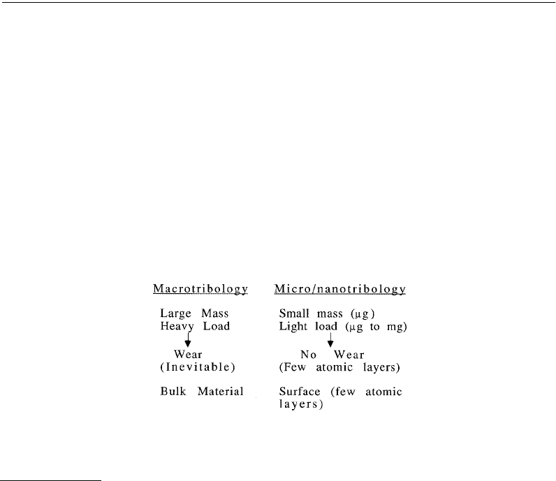
ventional or macrotribology and micro/nanotribology are contrasted in Figure
1.2. In macrotribology,
tests are conducted on components with relatively large mass under heavily loaded conditions. In these
tests, wear is inevitable and the bulk properties of mating components dominate the tribological perfor-
mance. In micro/nanotribology, measurements are made on components, at least one of the mating
components, with relatively small mass under lightly loaded conditions. In this situation, negligible wear
occurs and the surface properties dominate the tribological performance.
The micro/nanotribological studies are needed to develop fundamental understanding of interfacial
phenomena on a small scale and to study interfacial phenomena in micro
-
and nanostructures used in
FIGURE 1.2
Comparisons between macrotribology and micro/nanotribology.

© 1999 by CRC Press LLC
magnetic storage systems, MEMS, and other industrial applications. The components used in micro-
and nanostructures are very light (on the order of a few micrograms) and operate under very light loads
(on the order of a few micrograms to a few milligrams). As a result, friction and wear (on a nanoscale)
of lightly loaded micro/nanocomponents are highly dependent on the surface interactions (few atomic
layers). These structures are generally lubricated with molecularly thin films. Micro- and nanotribological
techniques are ideal for studying the friction and wear processes of micro- and nanostructures. Although
micro/nanotribological studies are critical to study micro- and nanostructures, these studies are also
valuable in the fundamental understanding of interfacial phenomena in macrostructures to provide a
bridge between science and engineering. At interfaces of technological innovations, contact occurs at
multiple asperity contacts. A sharp tip of a tip-based microscope sliding on a surface simulates a single
asperity contact, thus allowing high-resolution measurements of surface interactions at a single asperity
contact. Friction and wear on micro- and nanoscales have been found to be generally small compared
to that at macroscales. Therefore, micro/nanotribological studies may identify regimes for ultralow
friction and near zero wear.
To give a historical perspective of the field, the scanning tunneling microscope (STM) developed by
Dr. Gerd Binnig and his colleagues in 1981 at the IBM Zurich Research Laboratory, Forschungslabor, is
the first instrument capable of directly obtaining three-dimensional images of solid surfaces with atomic
resolution (Binnig et
al., 1982). Binnig and Rohrer received a Nobel prize in physics in 1986 for their
discovery. STMs can only be used to study surfaces which are electrically conductive to some degree.
Based on their STM design in 1985, Binnig et
al. developed an atomic force microscope (AFM) to measure
ultrasmall forces (less than 1
µN) present between the AFM tip surface and the sample surface (Binnig
et
al., 1986a, 1987). AFMs can be used for measurement of
all engineering surfaces
which may be either
electrically conducting or insulating. AFM has become a popular surface profiler for topographic mea-
surements on micro- to nanoscale (Bhushan and Blackman, 1991; Oden et
al., 1992; Ganti and Bhushan,
1995; Poon and Bhushan, 1995; Koinkar and Bhushan, 1997a; Bhushan et al., 1997c). Mate et
al. (1987)
were the first to modify an AFM in order to measure both normal and friction forces, and this instrument
is generally called friction force microscope (FFM) or lateral force microscope (LFM). Since then, a
number of researchers have used the FFM to measure friction on micro- and nanoscales (Erlandsson
et
al., 1988a,b; Kaneko, 1988; Blackman et
al., 1990b; Cohen et
al., 1990; Marti et
al., 1990; Meyer and
Amer, 1990b; Miyamoto et
al., 1990; Kaneko et
al., 1991; Meyer et
al., 1992; Overney et
al., 1992; Germann
et
al., 1993; Bhushan et
al., 1994a–e, 1995a–g, 1997a–b; Frisbie et
al., 1994; Ruan and Bhushan, 1994a–c;
Koinkar and Bhushan, 1996a–c, 1997a,c; Bhushan and Sundararajan, 1998). By using a standard or a
sharp diamond tip mounted on a stiff cantilever beam, AFMs can be used for scratching, wear, and
measurements of elastic/plastic mechanical properties (such as indentation hardness and modulus of
elasticity) (Burnham and Colton, 1989; Maivald et
al., 1991; Hamada and Kaneko, 1992; Miyamoto et
al.,
1991, 1993; Bhushan, 1995; Bhushan et
al., 1994b–e, 1995a–f, 1996, 1997a,b; Koinkar and Bhushan,
1996a,b, 1997b,c; Kulkarni and Bhushan, 1996a,b, 1997; DeVecchio and Bhushan, 1997).
AFMs and their modifications have also been used for studies of adhesion (Blackman et
al., 1990a;
Burnham et
al., 1990; Ducker et
al., 1992; Hoh et
al., 1992; Salmeron et
al., 1992, 1993; Weisenhorn et
al.,
1992; Burnham et
al., 1993a,b; Hues et
al., 1993; Frisbie et
al., 1994; Bhushan and Sundararajan, 1998),
electrostatic force measurements (Martin et
al., 1988; Yee et
al., 1993), ion conductance and electrochem-
istry (Hansma et
al., 1989; Manne et
al., 1991; Binggeli et
al., 1993), material manipulation (Weisenhorn
et
al., 1990; Leung and Goh, 1992), detection of transfer of material (Ruan and Bhushan, 1993), thin-
film boundary lubrication (Blackman et
al., 1990a,b; Mate and Novotny, 1991; Mate, 1992; Meyer et
al.,
1992; O’Shea et
al., 1992; Overney et
al., 1992; Bhushan et al., 1995f,g; Koinkar and Bhushan, 1996b–c),
to measure lubricant film thickness (Mate et
al., 1989, 1990; Bhushan and Blackman, 1991; Koinkar and
Bhushan, 1996c), to measure surface temperatures (Majumdar et
al., 1993; Stopta et al., 1995), for
magnetic force measurements including its application for magnetic recording (Martin et
al., 1987b;
Rugar et
al., 1990; Schonenberger and Alvarado, 1990; Grutter et
al., 1991, 1992; Ohkubo et
al., 1991;
Zuger and Rugar, 1993), and for imaging crystals, polymers, and biological samples in water (Drake
et
al., 1989; Gould et
al., 1990; Prater et
al., 1991; Haberle et
al., 1992; Hoh and Hansma, 1992). STMs

© 1999 by CRC Press LLC
have been used in several different ways. They have been used to image liquids such as liquid crystals
and lubricant molecules on graphite surfaces (Foster and Frommer, 1988; Smith et
al., 1989, 1990; Andoh
et
al., 1992), to manipulate individual atoms of xenon (Eigler and Schweizer, 1990) and silicon (Lyo and
Avouris, 1991), in formation of nanofeatures by localized heating or by inducing chemical reactions
under the STM tip (Abraham et
al., 1986; Silver et
al., 1987; Albrecht et
al., 1989; Mamin et
al., 1990;
Utsugi, 1990; Hosoki et
al., 1992; Kobayashi et
al., 1993), and nanomachining (Parkinson, 1990). AFMs
have also been used for nanofabrication (Majumdar et
al., 1992; Bhushan et
al., 1994b–e, Bhushan, 1995,
1997; Boschung et
al., 1994; Tsau et
al., 1994) and nanomachining (Delawski and Parkinson, 1992).
Instruments that are able to measure tunneling current and forces simultaneously are being custom
built (Specht et
al., 1991; Anselmetti et
al., 1992). Coupled AFM/STM measurements are made to dis-
tinguish between the topography of a sample and its electronic structure. Another aim is to determine
the role of pressure in the tunnel junction in obtaining STM images.
Surface force apparatuses (SFA) are used to study both static and dynamic properties of the molecularly
thin liquid films sandwiched between two molecularly smooth surfaces. Tabor and Winterton (1969) and
later Israelachvili and Tabor (1972) developed apparatuses for measuring the van der Waals forces between
two molecularly smooth mica surfaces as a function of separation in air or vacuum. These techniques
were further developed for making measurements in liquids or controlled vapors (Israelachvili and
Adams, 1978; Klein, 1980; Tonck et
al., 1988; Georges et
al., 1993). Israelachvili et
al. (1988), Homola
(1989), Gee et
al. (1990), Homola et
al. (1990, 1991), Klein et
al. (1991), and Georges et
al. (1994)
measured the dynamic shear response of liquid films. Recently, new friction attachments were developed
which allow for two surfaces to be sheared past each other at varying sliding speeds or oscillating
frequencies, while simultaneously measuring both the friction forces and normal forces between them
(Van Alsten and Granick, 1988, 1990a,b; Peachey et
al., 1991; Hu et
al., 1991). The distance between two
surfaces can also be independently controlled to within
± 0.1
nm and the force sensitivity is about 10
–8
N.
The SFAs are being used to study the rheology of molecularly thin liquid films; however, the liquid
under study has to be confined between molecularly smooth, optically transparent surfaces with radii of
curvature on the order of 1
mm (leading to poorer lateral resolution as compared with AFMs). SFAs
developed by Tonck et
al. (1988) and Georges et
al. (1993, 1994) use an opaque and smooth ball with a
large radius (~3
mm) against an opaque and smooth flat surface. Only AFMs/FFMs can be used to study
engineering surfaces
in the
dry and wet conditions
with
atomic resolution
.
The interest in the micro/nanotribology field grew from magnetic storage devices and its applicability
to MEMS is clear. In this chapter, we first describe various measurement techniques, and then we present
the examples of magnetic storage devices and MEMS where micro/nanotribological tools and techniques
are essential for interfacial studies. We then present examples of why micro/nanotribological studies are
important in magnetic storage devices, MEMS, and other microcomponents.
1.3 Measurement Techniques
The family of instruments based on STMs and AFMs are called scanning probe microscopes (SPMs).
These include STM, AFM, FFM (or LFM), scanning magnetic microscopy (SMM) (or magnetic force
microscopy, MFM), scanning electrostatic force microscopy (SEFM), scanning near-field optical micros-
copy (SNOM), scanning thermal microscopy (SThM), scanning chemical force microscopy (SCFM),
scanning electrochemical microscopy (SEcM), scanning Kelvin probe microscopy (SKPM), scanning
chemical potential microscopy (SCPM), scanning ion conductance microscopy (SICM), and scanning
capacitance microscopy (SCM). The family of instruments which measures forces (e.g., AFM, FFM, SMM,
and SEFM) are also referred to as scanning force microscopics (SFM). Although these instruments offer
atomic resolution and are ideal for basic research, they are also used for cutting-edge industrial applica-
tions which do not require atomic resolution. Commercial production of SPMs started with STM in
1988 by Digital Instruments, Inc., and has grown to over $100
million in 1993 (about 2000 units installed
to 1993) with an expected annual growth rate of 70%. For comparisons of SPMs with other microscopes,
see Table
1.1 (Aden, 1994). The numbers of these instruments are equally divided among the U.S., Japan,