Wong H.-S.P., Akinwande D. Carbon Nanotube and Graphene Device Physics
Подождите немного. Документ загружается.

3.5 Tight-binding energy dispersion 59
overlap matrix reduces to
S
AA
(k) =
∗
A
A
dr =
1
N
N
j
N
l
e
−ik·R
A
j
e
ik·R
A
l
×
φ
∗
(r − R
A
j
)φ(r − R
A
l
)dr (3.26)
S
AA
=
1
N
N
j
N
l
e
ik·(R
A
l
−R
A
j
)
δ
jl
= 1, (3.27)
where we have taken advantage of the normalized feature of Wannier functions,
φ
∗
(r − R
j
)φ(r − R
j
)dr = 1.
2. Electron–hole symmetry: A close observation of the ab-initio dispersion in the
neighborhood of the Fermi energy (E = 0 at the K-point in Figure 3.6) reveals
that the π and π
∗
branches have similar structure, at least for energies close
to the E
F
. Within this restricted range, the energy branches are approximately
mirror images of each other. Since electrons are the mobile charges in the π
∗
band and holes are the mobile charges in the π band, we call this approximation
the electron–hole symmetry.
12
Obviously, from Figure 3.6 this symmetry does
not hold over a large range of energies. Nonetheless, this approximation is very
useful because much of the electron dynamics in practical devices occur over
a relatively small range of energies close to the Fermi energy. Mathematically,
electron–hole symmetry forces S
AB
(k) = 0. This is not immediately obvious,
but can be seen (after some deep thought) by observing that the only part of
Eq. (3.22) that possesses symmetry about some numberis theplus/minus square
root argument, i.e. −
f (k) is a mirror image of +
f (k). In order for Eq. (3.22)
to retain this symmetry, S
AB
(k) must vanish to zero. Therefore:
E(k)
±
= E
2p
±
H
AB
(k)H
∗
AB
(k), (3.28)
which is the energy dispersion originally proposed by Wallace in 1947.
13
The
electron–hole symmetry argument is somewhat subtle yet powerful in simpli-
fying Eq. (3.22) without compromising on accuracy, particularly at energies
close to E
F
.
We can go one step further to simplify Eq. (3.28) without any loss of accuracy by
setting E
2p
= 0. This is because energy is naturally defined to within an arbitrary
reference potential. For the case of graphene, the reference potential is the Fermi
energy (a parameter independent of k) and is customarily set to 0 eV. Since the
12
A key physical outcome of this symmetry is that electrons and holes will have identical
equilibrium properties, such as density of states, group velocity, and carrier density.
13
P. R. Wallace, The band theory of graphite. Phys. Rev., 71 (1947) 622–34.
60 Chapter 3 Graphene
only parameter independent of k in Eq. (3.28)isE
2p
, it is convenient to employ
it as the reference and hence E
2p
= E
F
= 0 eV. Finally, we arrive at
E(k)
±
=±
H
AB
(k)H
∗
AB
(k). (3.29)
The Hamiltonian matrix element H
AB
(k) can be calculated in a straightforward
manner, though is somewhat algebraically tedious:
H
AB
(k) =
∗
A
H
B
dr =
1
N
N
j
N
l
e
−ik·(R
A
j
−R
B
l
)
×
φ
∗
(r − R
A
j
)H φ(r − R
B
l
)dr (3.30)
As a result of the NNTB stipulations, each type-A atom will only overlap with its
three nearest neighbors, which are type B. It is convenient to define the nearest
neighbor distances between a type-A atom and its three type-B atoms. Let these
nearest neighbor distances be R
1
= R
Aj
− R
Bj
, R
2
= R
Aj
− R
Bj+1
, R
3
=
R
Aj
−R
Bj−1
(as denoted in Figure 3.4), where j, j +1, and j −1 are the indices of
the primitive unit cells where the three type-B nearest neighbor atoms are located
with respect to atom A in cell j.
H
AB
(k) =
1
N
N
j
3
m=1
e
−ik·R
m
E
m
(3.31)
where E
m
is the finite value of the integration of the nearest neighbor Wannier
functions. By necessity E
1
= E
2
= E
3
, because the integrals are radially dependent
and the nearest neighbor distances are radially symmetric. For convenience we
can simply set E
m
= γ , which can be viewed as a fitting parameter of positive
value.
14
γ is often called by many names, including the nearest neighbor overlap
energy, the hopping or transfer energy, or the carbon–carbon interaction energy.
The Hamiltonian matrix element reduces to a sum of three terms:
H
AB
(k) = γ(e
−ik·R
1
+ e
−ik·R
2
+ e
−ik·R
3
) (3.32)
and
H
AB
(k)H
∗
AB
(k) = γ
2
(e
−ik·R
1
+ e
−ik·R
2
+ e
−ik·R
3
)(e
ik·R
1
+ e
ik·R
2
+ e
ik·R
3
),
(3.33)
14
Strictly speaking γ is a negative value owing to the sign convention for attractive potentials, and
some authors define it accordingly. Here, it is defined positive for convenience. Ultimately, the
polarity does not matter, provided the analysis is consistent.
3.5 Tight-binding energy dispersion 61
H
AB
(k)H
∗
AB
(k) = γ
2
[3 + e
ik·(R
1
−R
2
)
+ e
−ik·(R
1
−R
2
)
+ e
ik·(R
1
−R
3
)
+ e
−ik·(R
1
−R
3
)
+ e
2ik·(R
2
−R
3
)
+ e
−ik·(R
2
−R
3
)
], (3.34)
H
AB
(k)H
∗
AB
(k) = γ
2
{3 + 2 cos[k · (R
1
− R
2
)]+2 cos[k · (R
1
− R
3
)]
+ 2 cos[k · (R
2
− R
3
)]}, (3.35)
where Euler’s formula, e
ix
+ e
−ix
= 2 cos[x], has been used to simplify the
exponentials. The nearest neighbor distances are given by Eq. (3.2); thus:
H
AB
(k)H
∗
AB
(k) = γ
2
1 + 4 cos
√
3a
2
k
x
cos
a
2
k
y
+ 4 cos
2
a
2
k
y
. (3.36)
And hence our central mission in deriving analytically the π bands of graphene
can now be accomplished by inserting Eq. (3.36) into Eq. (3.29):
E(k)
±
=±γ
1 + 4 cos
√
3a
2
k
x
cos
a
2
k
y
+ 4 cos
2
a
2
k
y
. (3.37)
This formula is the widely used NNTB approximation from which CNT band
structure is derived. The precise value of γ is difficult to determine analytically;
as such, it is often used as a fitting parameter to match ab-initio computations
or experimental data. Commonly used values for γ range from about 2.7 eV to
3.3 eV. For routine calculations, the extracted value γ ≈ 3. 1 eVfrom experimental
measurements of the Fermi (or group) velocity (v
F
≈ 10
6
ms
−1
) in graphene is
adequate.
15
It is particularly of interest to identify the highest energy state within
the valence band and the lowest energy state within the conduction band. These
states occur at the K-point corresponding to E = 0eV.
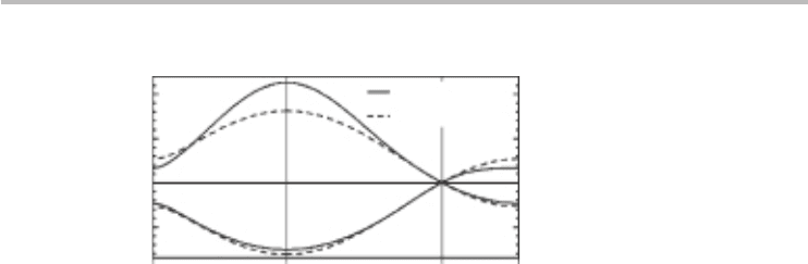
Comparison of the NNTB dispersion, Eq. (3.37), with ab-initio computations
for the π bands shows good agreement (Figure 3.7) with the strongest agree-
ment expectedly at low energies.
16
A greater agreement at higher energies can be
achieved by relaxing the electron–hole symmetry approximation, which leads to
a non-zero S
AB
(k). For this case, it can be shown that the energy dispersion is
E(k)
±
=
±γ
1 + 4 cos
√
3a
2
k
x
cos
a
2
k
y
+ 4 cos
2
a
2
k
y
1 ∓ s
o
1 + 4 cos
√
3a
2
k
x
cos
a
2
k
y
+ 4 cos
2
a
2
k
y
(3.38)
15
Theoretically, v
F
is proportional to γ . See R. S. Deacon, K.-C. Chuang, R. J. Nicholas,
K. S. Novoselov and A. K. Geim, Cyclotron resonance study of the electron and hole velocity in
graphene monolayers. Phys. Rev. B, 76 (2007) 081406.
16
Energies close to the Fermi energy are referred to as low energies. There is no standard definition
of how close is close enough, but a range within ±1 eV is sometimes considered reasonable. In
general, the range is application dependent.
62 Chapter 3 Graphene
MK
Γ
M
Wavevector
10
ab initio
tight binding
Energy (eV)
5
0
–5
Fig. 3.7 Comparison of ab-initio and NNTB dispersions of graphene showing good agreement at
low energies (energies about the K-point). γ = 2.7 eV and s
o
= 0 are used. Courtesy of
S. Reich, J. Maultzsch and C. Thomsen, Phys. Rev. B, 66 (2002) 35412. Adapted with
permission from S. Reich, J. Maultzsch and C. Thomsen, Phys. Rev. B, 66 (2002) 35412.
Copyright (2002) by the American Physical Society.
where s
o
is called the overlap integral and is often employed as a fitting parameter
with a value that is positive and nominally close to zero (compared with unity).
The use of two fitting parameters (γ , s
o
) will inevitably lead to a better overall
agreement. Much of the exploration of graphene and derived nanostructures such
as CNTs has been focused on the low-energy properties and dynamics; as such,
we will use Eq. (3.37) in the remainder of our discussions unless noted otherwise.
Fermi energy
The equilibrium Fermi energy is the energy of the highest occupied k-state when
the solid is in its ground or rest state (temperature 0 K). Determining E
F
involves
populating the k-states in the Brillouin zone with all the π-electrons in the solid
according to Pauli’s exclusion principle. There are Nk-states in the valence band,
which can hold 2N electrons, including spin degeneracy. Each carbon atom pro-
vides one p
z
electron, resulting in two electrons/unit cell. Since there are N unit
cells, we have a total of 2N electrons which will fill up the valence band. It fol-
lows that the highest occupied state housing the most energetic electrons are at the
K-points, as identified earlier, and the corresponding energy is formally defined
as the Fermi energy (E
F
= 0 eV). The properties of electrons around the Fermi
energy often determine the characteristics of practical electronic devices.
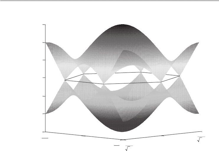
Figure 3.8 shows the 3D plot of the NNTB dispersion throughout the Brillouin
zone. The upper half of the dispersion is the conduction (π
∗
) band and the lower
half is the valence (π ) band. Owing to the absence of a bandgap at the Fermi
energy, and the fact that the conduction and valence bands touch at E
F
, graphene is
considered a semi-metal or zero-bandgap semiconductor, in contrast to a regular
metal, where E
F
is typically in the conduction band, and a regular semiconductor,
where E
F
is located inside a finite bandgap.
3.6 Linear energy dispersion and carrier density 63
0
0
–3
–2
–1
0
1
2
3
E/y
o
k
x
k
y
a3
2
π
3a
2
π
−
3a
4
π
3a
4
π
Fig. 3.8 The nearest neighbor tight-binding band structure of graphene. The hexagonal Brillouin
zone is superimposed and touches the energy bands at the K-points.
Under non-equilibrium conditions (applied electric or magnetic fields) or extrin-
sic conditions (presence of impurity atoms), the Fermi energy will depart from its
equilibrium value of 0 eV. The deviation of E
F
from its equilibrium value is often
valuable in determining the strength of the field or concentration of impurity atoms.
3.6 Linear energy dispersion and carrier density
The behavior of graphene electrons at the Fermi energy is of significant interest
in condensed matter physics, particularly because the band structure has a linear
dispersion which is representative of so-called massless particles (particles with
zero effectivemass).
17,18
For massless particles, Einstein’sspecial relativity comes
into play in the form of Dirac’s relativistic quantum mechanical wave equation
for describing the particle dynamics. Thus, the six K-points in graphene where the
conduction and valence bands touch are frequently called the Dirac points (keep
in mind that the energy at these points is, of course, E
F
) in the physics literature.
17
A linear relation between energy and momentum or wavevector formally defines a massless
relativistic particle. Examples of massless (or approximately massless) relativistic particles
include photons and neutrinos. The idea of effective mass will be formally introduced in Chapter 5.
18
Massless electron waves also exist in a relatively new state of quantum matter called topological
insulators. See Y. L. Chen et al., Experimental realization of a three-dimensional topological
insulator, Bi
2
Te
3
. Science, 325 (2009) 178–81.
64 Chapter 3 Graphene
k
x
k
y
E
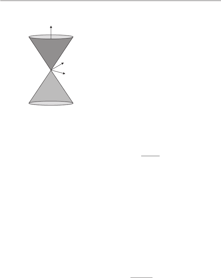
Fig. 3.9 The linear energy dispersion of graphene at the K-point which is known as the Dirac cone.
At these K-points and energies close by, the dispersion centered at the K-point can
simply be expressed as a linear equation:
E(k)
±
linear
=±v
F
|k|=±v
F
k
2
x
+ k
2
y
=±v
F
k, (3.39)
where k is now in spherical coordinates, is the reduced Planck’s constant, and
the Fermi velocity is defined as v
F
= (1/)(∂E/∂k) evaluated at the Fermi energy.
It follows that v
F
is the gradient of the dispersion. A 3D plot of the linear dis-
persion is the celebrated Dirac cone shown in Figure 3.9. The linear dispersion
has been confirmed up to approximately ±0.6 eV by experimental spectroscopic
measurements.
19
A central property of electronic materials is the density of states (DOS) g(E),
which informs us of the density of mobile electrons or holes present in the solid
at a given temperature. Formally, in two dimensions, the total number of states
available between an energy E and an interval dE is given by the differential area in
k-space dA divided by the area of one k-state. Mathematically, this is equivalent to
g(E)dE = 2g
z
dA
(2π)
2
/
, (3.40)
where the factor of two in the numerator is included for spin degeneracy, g
z
is the
zone degeneracy, and is the area of the lattice. There are six equivalent K-points,
and each K-point is shared by three hexagons; therefore, g
z
= 2 for graphene. To
determine dA, let us consider a circle of constant energy in k-space. The perimeter
of the circle is 2πk and the differential area obtained by an incremental increase
19
I. Gierz, C. Riedl, U. Starke, C. R. Ast and K. Kern, Atomic hole doping of graphene. Nano Lett.,
8 (2008) 4603.
3.6 Linear energy dispersion and carrier density 65
of the radius by dk is 2πkdk.
20
Therefore, the DOS, which is always a positive
value or zero, is
g(E) =
2
π
k
dk
dE
=
2
π
k
dE
dk
−1
, (3.41)
where g(E) has been normalized to the . Substituting from Eq. (3.39) yields a
linear DOS appropriate for low energies:
g(E) =
2
π(v
F
)
2
|E|=β
g
|E|, (3.42)
where β
g
is a material constant, β
g
≈ 1.5 × 10
14
eV
−2
cm
−2
= 1.5 ×
10
6
eV
−2
µm
−2
, and the absolute value of E is necessary because energy can
be either positive (electrons) or negative (holes). At the Fermi energy (E
F
= 0),
the DOS vanishes to zero even though there is no bandgap. This is the reason why
graphene is considered a semi-metal in contrast to regular metals that have a large
DOS at the Fermi energy.
The electron carrier density is simply the number of states that are occupied per
unit area at a given temperature. The occupation probability for electrons at finite
temperatures is given by the Fermi–Dirac distribution:
f (E
F
) =
1
1 + e
(E−E
F
)/k
B
T
(3.43)
where k
B
is Boltzmann’s constant and T is the temperature. The equilibrium
electron carrier density n is
n =
E
max
0
g(E)f (E
F
) dE =
2
π
2
v
2
F
E
max
0
E
1 + e
(E−E
F
)/k
B
T
dE (3.44)
where E
max
is the maximum energy in the energy band. For the majority of appli-
cations of interest the Fermi energy is often much less than E
max
, and owing to
the exponential decay of the Fermi–Dirac distribution for energies greater than
E
F
, simply setting E
max
to infinity introduces negligible error. Additionally, let
η = E
F
/k
B
T and η
F
= E
F
/k
B
T for mathematical convenience:
n =
2
π
kT
v
F
2
∞
0
η
1 + e
η−η
F
dη =
2
π
kT
v
F
2
F
1
(E
F
/k
B
T ), (3.45)
20
The differential area can be visualized as the difference between the area of a circle of radius
k + dk and a circle of radius k in the limit when dk is very small.
66 Chapter 3 Graphene
with F
1
(·) representing the Fermi–Dirac integral of order one.
21
In general, F
1
(·)
is an infinite series which is non-analytic but can be expressed in a closed form for
a limited range of E
F
/k
B
T by employing Taylor series expansion or other suitable
approximation techniques. For the special case of an intrinsic graphene sheet with
no doping of any kind, the Fermi energy is at 0 eV independent of temperature,
resulting in an exact value of π
2
/12 for the Fermi–Dirac integral. Therefore, the
intrinsic carrier density n
i
is
n
i
=
π
6
k
B
T
v
F
2
≈ 9 ×10
5
T
2
(electrons/cm
2
), (3.46)
with T in units of kelvin. It is worthwhile noting that the intrinsic carrier
density reveals a temperature-squared dependence in contrast to conventional
semiconductors, where n
i
has an exponential dependence on temperature. Notice-
ably, the only material dependence is the Fermi velocity. At room temperature,
n
i
≈ 8 ×10
10
cm
−2
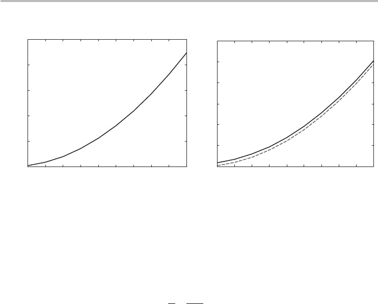
. The intrinsic carrier density is plotted in Figure 3.10a.
For an extrinsic material that has been doped with impurities for example, it
is often desirable to have a simple closed-form equation for the extrinsic carrier
density n
e
as a function of E
F
. Fortunately, an approximate algebraic formula is
available by considering the limit when E
F
/k
B
T →∞. In this limit:
n
e
∼
=
λ
π
E
F
v
F
2
, (3.47)
where λ is a fitting parameter. λ = 1.1 gives an error less than ±10 % for E
F
/k
B
T >
4, and λ = 1 gives an error less than 5 % for E
F
/k
B
T > 8. This serves as a useful
formula for extracting the Fermi energy for a given extrinsic doping concentration
that is much greater than the intrinsic carrier density. The extrinsic carrier density
is shown in Figure 3.10b.
Alternatively, a simple (approximate) formula that can be applied both for
thermal equilibrium conditions and at finite potentials is obtained by the linear
combination of the intrinsic and extrinsic expressions given by
n
∼
=
n
i
+
E
2
F
π(v
F
)
2
(3.48)
As a result of the electron–hole symmetry of the energy bands of graphene, the hole
carrier density p under intrinsic conditions is equal to the electron carrier density,
21
This specific Fermi–Dirac integral of order one is a form of alternating (infinite) power series that
has a quasi-quadratic curve. For hand-analysis, it might be more convenient to express the
Fermi–Dirac integral in terms of the polylogarithmic function, which is a standard mathematical
function and whose properties are much more understood.
3.7 Graphene nanoribbons 67
1 2 3 4 5 6 7 8 910
0
1
2
3
4
5
6
50 100 150 200 250 300 350 400 450 500
0
5
10
15
20
25
T (K)
Intrinsic carrier density (n
i
) x10
10
cm
–2
Extrinsic carrier density (n
e
) x10
12
cm
–2
E
F
/k
B
T
Fig. 3.10 (a) Intrinsic carrier density for graphene. (b) Extrinsic carrier density. The bold line
representstheexactcomputationofEq.(3.45)andthedashedlineistheapproximate
closed-formformulaofEq.(3.47).
and for extrinsic conditions the hole carrier density has equivalent structure to the
electron carrier density:
p =
2
π
k
B
T
v
F
2
F
1
(−E
F
/k
B
T ). (3.49)
3.7 Graphene nanoribbons
Graphene nanoribbons are narrow rectangles made from graphene sheets and have
widths on the order of nanometers up to tens of nanometers. The nanoribbons can
have arbitrarily long length and, as a result of their high aspect ratio, they are
considered quasi-1D nanomaterials. GNRs are a relatively new class of nano-
materials that can have metallic or semiconducting character, and are currently
being investigated for their interesting electrical, optical, mechanical, thermal,
and quantum-mechanical properties.
22
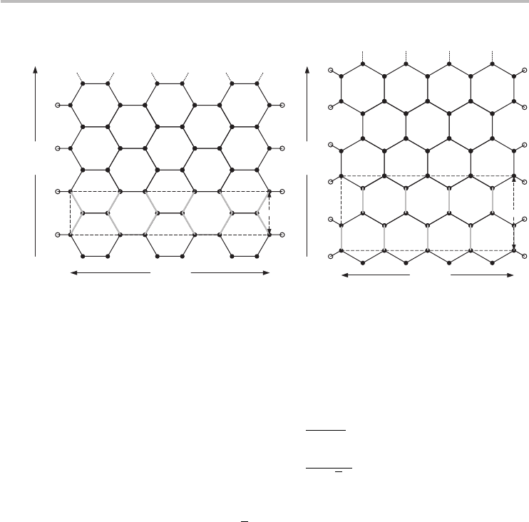
There are two types of ideal GNR, which are called armchair GNRs (aGNRs)
and zigzag GNRs (zGNRs). The GNR has an armchair cross-section at the edges,
while the zGNR has a zigzag cross-section, both illustrated in Figure 3.11.In
addition, the GNRs are also labeled by the number of armchair or zigzag chains
present in the width direction of the aGNR and zGNR respectively. Let N
a
be the
number of armchair chains and N
z
the number of zigzag chains, then the nanoribbon
can be conveniently denoted as N
a
-aGNR and N
z
-zGNR respectively. Figure 3.11
illustrates how to count the number of chains for a 9-aGNR and a 6-zGNR. The
22
For a recent review of nano-scale and micrometer-scale graphene science, see A. K. Geim and
K. S. Novoselov, The rise of graphene. Nat. Mater., 6 (2007) 183–91.
68 Chapter 3 Graphene
Length
1
2
3
4
5
6
7
8
N
a
=9
l
a
(b)
1 23 45N
z
=6
Length
Width(w)
Width(w)
l
z
(a)
Fig. 3.11
The finite-width honeycomb structure of GNRs. (a) The lattice of a 6-zGNR and (b) the
lattice of a 9-aGNR. The dashed box represents the primitive unit cell. The open circles at
the edges denote passivation atoms such as hydrogen. The bold gray lines are the zigzag
or armchair chains that are used to determine N
z
or N
a
respectively.
width of the GNRs can be expressed in terms of the number of lateral chains:
aGNR, w =
N
a
− 1
2
a, (3.50)
zGNR, w =
3N
z
− 2
2
√
3
a, (3.51)
where a = 2.46 Å is the graphene lattice constant as usual. The lengths of the
primitive unit cells are l
a
=
√
3a and l
z
= a for aGNRs and zGNRs respectively.
Non-ideal GNRs with mixed edge cross-sections may also exist, but those are not
as well understood.
The small width of GNRs can lead to quantum confinement of electrons which
restricts their motion to one dimension along the length of the nanoribbons, in
contrast to a large graphene sheet where electrons are free to move in a 2D
plane. As a result of several factors, including the quantum confinement, particu-
lar boundary conditions at the edges, and the effect of states arising from carbon
atoms at the edges (also known as edge states), the band structure of GNRs is
generally complex and departs significantly from that of the 2D graphene sheet.
The band structure of GNRs can be computed numerically using first principles
or tight-binding schemes.
23
The numerical computations reveal that zGNRs are
semiconductors with bandgaps that are inversely proportional to the nanoribbons,
width. Similarly, aGNRs also possess bandgaps which depend inversely on the
width and, additionally, have a dependence on the number of armchair chains in
23
See Y.-W. Son, M. L. Cohen and S. G. Louie, Energy gaps in graphene nanoribbons. Phys. Rev.
Lett., 97 (2006) 089901, and references contained therein. Currently, no accurate analytical
formula for the band structure is available.