Wong H.-S.P., Akinwande D. Carbon Nanotube and Graphene Device Physics
Подождите немного. Документ загружается.


7.12 Problem set 189
to ask for a method to produce all metallic nanotubes with identical diameters
for interconnect applications.
Unfortunately, we have yet to see the synthesis genie and for now we
have to deal with what we have. As such, a theory of nanotube resistance for
today’s growth methods must be statistical in nature for greatest relevance.
For simplicity, assume that somehow we stumbled upon a method to produce
only metallic nanotubes with a diameter dispersion (the next best thing com-
pared with our heart’s desire). Consider a Gaussian diameter dispersion, for
diameters ranging from d
t
∼ d
o
to 3d
o
, and centered halfway.
(a) For an interconnect that contains a large array of these nanotubes, what
is the average mean free path and resistance of the CNT interconnect for
low fields? For d
o
∼ 0.5 nm, provide numerical estimates. Assume room
temperature operation, l
d
∼ 10 µm and α
ac
∼ 400 ×10
3
K.
(b) What is the standard deviation of the mean free path and resistance?
(c) By good fortune we managed to wake up the synthesis genie, who granted
us our desires of an array of nanotubes with each CNT havinga1nm
diameter. Compare the mean free path and resistance of this array with
those of part (a).
7.4. Temperature dependance of CNT mean free path.
It is worthwhile to be mathematically fluent in routinely analyzing the
temperature dependence of the CNT mean free path and resistance.
(a) For this purpose, plot the low-field mean free path of l
ac
, l
d
, l
op,abs
, l
op,ems
,
and l
m,eff
for temperatures from 100 to 500 K. Use the values, E =
20 mV µm
−1
, E
op
= 0.16 eV, l
ac,300
= 1.6 µm,l
op,300
= 15 nm, and
l
d
= 50 µm.
(b) Show that, in the low-field limit, the effective mean free path is pro-
portional to ∼1/T below room temperature and ∼1/T
2
above room
temperature. What is responsible for the inverse power of 2 dependence
at higher temperatures compared with lower temperatures?
7.5. Single-wall versus multi-wall nanotubes.
Yes, nanotubes indeed compete with each other.Acase in point is for intercon-
nect applications. The pressing question is: Which type of nanotube provides
the best performance? To address this question we explore an example model
of both types of nanotube and restrict our attention to the low-field resistivity
for the diffusive case at room temperature. For single-wall CNTs, we consider
a dense square array of identical nanotubes (d
t
= 1 nm, array cross-section
has a height h), with a vertical and horizontal pitch. Also, the single-wall
CNT has an acoustic phonon mean free path ∼1 µm. For multi-wall CNTs,
d
in
= 6 nm, and d
out
= h.

190 Chapter 7 Carbon nanotube interconnects
(a) Derive the resistivity (classical resistivity in units of resistance-length)
for both types of nanotube. Plot their resistivities on the same graph
for h = 20 nm and 100 nm and for lengths from 100 nm to 100 µm.
Assume the effective mean free path of the MWCNT is ∼10 µm and
diameter dependent to first order. Which type of nanotube offers the
lowest resistivity? Also, determine which type of nanotube offers the
lowest capacitance.
(b) It was noted in the text that l
m,eff
of multi-wall nanotubes is currently a
matter of further research. As such, it is presently challenging to make a
fair comparison involving multi-wall nanotubes in general, since we will
have to assume some value for the mean free path. Obviously, very high
values might be overlyoptimistic and likewisevery low valuesmight lead
to negatively biased conclusions. Perhaps a compromise is to consider a
range of values for the mean free path to get a more complete comparative
picture. For this reason, let us restrict our attention to the diffusive limit,
which makes it easier to perform the subsequent analysis. What is the
expression for the resistivity of the MWCNT in this limit for an arbitrary
l
m,eff
?
(c) Plot the resistivity of both the single-wall and multi-wall nanotubes in
the diffusive limit as a function of the multi-wall l
m,eff
ranging from
1to100µm. From this plot, what can you conclude about the resistance
of MWCNTs compared with single-wall CNTs for interconnect applica-
tions? Extend your qualitative conclusions to include comparisons with
copper interconnects of the same cross-section.

8 Carbon nanotube field-effect
transistors
Innovation is everything. When you are on the forefront, you can see what
the next innovation needs to be.
Robert Noyce (co-inventor of integrated circuits and co-founder of Intel)
8.1 Introduction
In analogy to a water pipe that allows the guided flow of water, a transistor is an
electronic device that allows for the guided flow of electrons with the key innova-
tion being the influence of a gate that controls the amount of flowing electrons (the
gate is similar in concept to a valve controlling the amount of water). The most pop-
ular flavor ofthe transistor is the field-effect transistor (FET), which came to reality
in 1960
1
and forms the cornerstone of modern electronics that has revolutionized
computing, communications, automation, and healthcare and fosters today’s digital
lifestyles. In part due to the continuous miniaturization or scaling of the transistor
dimensions,
2
silicon (Si) has evolved to be the de facto semiconductor for making
transistors that enable smaller, faster, cheaper, and more power-efficient integrated
circuits (also called chips) for an extensive variety of applications. However, tran-
sistor scaling and the resulting performance enhancement cannot continue forever
owing to both physical and technical reasons. Obviously, the transistor cannot be
reduced to a size of zero length for example, and this imposes a physical limit to the
miniaturization of devices. Fortunately, we have yet to reach this physical limit. At
present, the more pressing issues are technical in nature: relating to the challenges
of fabricating small transistors and, in addition, the significance at short size scales
1
Interestingly, the FET was patented in 1926 by physicist Julius Lilienfeld. However, it took almost
35 years before a practical FET could be realized, partly because of the presence of surface states
that usurped the influence of the gate. This issue was finally resolved in 1960 (at Bell Labs) by
passivating the (silicon) semiconductor surface with an oxide (SiO
2
). This brings to life the words
of the anonymous writer, “Persistence is the twin sister of excellence. One is a matter of quality
(innovation), the other, a matter of time (realization).”
2
The great benefits of the scaling that has driven semiconductor technology over the past four
decades was brought to light in the celebrated work of Robert Dennard and coworkers. See
R. H. Dennard, F. H. Gaensslen, H.-N. Yu, V. L. Ridoout, E. Bassous and A. R. LeBlanc, Design of
ion-implanted MOSFET’s with very small physical dimensions. IEEE J. Solid-State Circuits, 9
(1974) 25–68. Previously, Dennard had invented the DRAM memory cell.

192 Chapter 8 Carbon nanotube field-effect transistors
of some otherwise undesirable device phenomena which are collectively referred
to as short-channel or small-dimension effects.
3
Largelydue to thescaling challenges facingsilicon transistors, thereare substan-
tial efforts to explore promising nanomaterials as candidates for future transistors
with an implicit requirement that these nanomaterials not only produce transistors
that scale gracefully (i.e. not sensitive to short-channel effects) at the nanoscale,
but also offer higher performance at comparable length scales. This was the his-
toric motivation for researching carbon nanotube field-effecttransistors (CNFETs),
where the semiconducting material is a (semiconducting) CNT. The experimental
observation of ballistic electron transport over relatively long lengths in CNTs
plus their higher current density and projected faster speed certainly make a com-
pelling case for CNFETs as exploratory transistors. At the same time, CNTs, still
being relatively new on the scene, deserve to be studied for their own sake as
well, for a variety of reasons, including a necessary need to learn new paradigms
about what nature offers in one dimension and the potential for new applications
beyond the reach of conventional semiconductors. Hence, a comprehensive theory
of the device physics of CNFETs is clearly of broad significance and interest that
transcends the historical motivation.
The discussion begins with a survey of typical CNFET device geometries and
the basic operating principles. Afterwards, an expression for the all-important
CNT surface potential is developed. The middle sections of the chapter elucidate
the theory of the device physics of CNFETs and comparisons with experimental
results are examined. The chapter concludes by shining light on the paradigm shift
between a 1D FET and its 2D counterpart. Much of the content from the previous
chapters will be useful to the reader, with the lion’s share of the content courtesy of
Chapters6and7.Abasicunderstandingofsilicontransistordevicephysics,while
not required for understanding many of the ideas in this chapter, will nonetheless
only help the reader in gaining broader and deeper insights. For example, basic
device physics concepts such as energy band diagrams, workfunction, and flatband
voltage will be a part of the narrative without any elementary introduction. The
reader will find supplementary readings convenient to fill in any information gap.
3,4
8.2 Survey of CNFET device geometries
Carbon nanotube FETs can be realized in several geometrical configurations. The
most common device geometries are shown in Figure 8.1. The device geometries
3
See Y. Taur and T. H. Ning, Fundamentals of Modern VLSI Devices, 2nd edn (Cambridge
University Press, 2008).
4
There are many outstanding texts, including R. F. Pierret, Semiconductor Device Fundamentals
(Addison-Wesley, 1996); and B. G. Streetman and S. Banerjee, Solid-State Electronic Devices, 6th
edn (Prentice Hall, 2005).
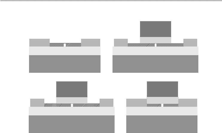
8.2 Survey of CNFET device geometries 193
G
High-k
S D
G
High-k
(a) (b)
SiO
2
Si
SiO
2
Si
S D
S D
SiO
2
p++ Si (BG) p++ Si (BG)
i
G
High-k
SiO
2
S D
(c) (d)
n++ n++
i
i
i
Fig. 8.1
Cross-sectional illustrations of four common CNFET device geometries. (a) A back-gated
CNFET with the heavily doped Si substrate serving as the gate (p++ refers to heavy hole
doping). (b) CNFET featuring both a top-gate and a back-gate. The top-gate is used to
control the channel and the back-gate is used to (electrostatically) dope the CNT extension
regions to achieve a low-resistance path to the S/D contacts. (c) A CNFET with
chemically doped nanotube extension regions. (d) A self-aligned CNFET. Note that “i”
represents an intrinsic semiconducting CNT.
all have certain familiar features, including an intrinsic (undoped) semiconducting
nanotube serving as the channel, source (S) and drain (D) metallic contacts, a gate
(G) electrode appearing in the form of a top-gate or a back-gate (BG), and an oxide
or high-k dielectric,
5
to insulate the gate from the CNT. The operating dynamics
of all the CNFET devices are very similar. The gate controls the amount of charge
in the channel via a vertical electric field that induces either electrons or holes in
the nanotube, while a horizontal electric field between the contacts provides the
force that drives the charges from one contact to the other, resulting in an electric
current. A top-gate is often preferred over a back-gate to provide localized and
greater control of the nanotube channel, as well as to afford individual gate control
in a multi-transistor circuit.
Figure 8.1a illustrates the most basic CNFET device geometry, where a heavily
doped substrate serves asthe gate. The CNFET device in Figure 8.1b hasthe unique
distinction of featuring botha top-gate anda back-gate. To avoid anyambiguity, the
actual semiconducting channel is the section of the nanotube directly underneath
the top-gate. In this configuration, the top-gate is the main gate used to control the
charge density in the nanotube channel, while the back-gate is employed to convert
5
High-k dielectric is a fondly used jargon in the field of semiconductor physics. In a nutshell, it
refers to dielectrics that possess a relative dielectric constant (k or ε
r
) several times greater than
that of SiO
2
(k = 3.9).

194 Chapter 8 Carbon nanotube field-effect transistors
the semiconducting nanotube extension regions into quasi-metallic conductors in
order to provide a low-resistance path between the channel and the metal contacts.
This conversion is achieved by applying a sufficiently high back-gate voltage
which creates a vertical electric field and induces excess electrons or holes in the
CNT extension regions, a technique otherwise known as electrostatic doping. The
CNFET device in Figure 8.1c is similar to that of Figure 8.1b, with chemical dop-
ing of the CNT extension regions instead of electrostatic doping. Figure 8.1dis
an illustration of a self-aligned top-gated CNFET. It is referred to as self-aligned
because, during fabrication, the gate metal is deposited first and subsequently used
to align the source/drain metals, resulting in zero horizontal gap (or no extension
regions) between the gate and the source/drain contacts. The self-alignment can be
achieved in practice by exploiting the native oxide,
6
which forms on the surface of
many metals when exposed to air or oxygen. For example, aluminum easily forms
a native aluminum oxide (Al
2
O
3
). This native oxide around the gate metal is the
enabling technique in obtaining self-alignment while providing electrical isolation
between the gate and source/drain metals. Even though the CNFET devices shown
in Figure 8.1 are supported by an SiO
2
/Si substrate, it is entirely possible to employ
a different substrate (for example, quartz or flexible substrates). The choice of sil-
icon substrates is in part due to the advantages and convenience of leveraging the
mainstream fabrication infrastructure that has been developed around bulk silicon.
Similarly, the types of free carrier in the CNFET devices can be either holes (p++)
or electrons (n++). A silicon substrate serving as a back-gate is often doped with
holes because a lower substrate resistance can be achieved.
In general, charge transport in a CNFET can be categorized into four regimes
regardless of the specificdevice geometry.The four transport regimes areidentified
in Table 8.1. They are determined by the length of the nanotube compared with
their mean free path l
m
and by the type of contact the nanotube makes with the
source/drain metals. For example, an ohmic-contact ballistic CNFET refers to
the case where charge injection from the S/D contacts into the CNT and vice
versa is ohmic in nature (i.e. a simple resistance), and the charges travel through
the nanotube channel without experiencing scattering. Conversely, a Schottky-
barrier diffusive CNFET refers to a device where charges experience a Schottky
barrier at the S/D nanotube junction, and charge transport through the nanotube
channel suffers from repeated scattering. Charge can refer equally to electrons
and/or holes. If electrons are the majority charge carriers, then the CNFET is an
n-type transistor; and if holes are the majority carriers, then the CNFET is a p-type
transistor. Quite intriguingly (and often undesired), it is also fairly easy to observe
the so-called ambipolar behavior in CNFETs, where electrons are the majority
6
A thin oxide, of the order of 1 nm, readily forms on the surface of many metals through the process
of oxidation in the presence of air or oxygen. This natural thin oxide is what is called the native
oxide.

8.3 Surface potential 195
Table 8.1. The four transport regimes of CNFETs
Metal–CNT contact L < l
m
L > l
m
Ohmic Ohmic-contact ballistic CNFET Ohmic-contact diffusive CNFET
Schottky barrier Schottky-barrier ballistic CNFET Schottky-barrier diffusive CNFET
charges for positive gate voltages and holes are the majority charges for negative
gate voltages.
7
This is in part due to their low bandgap.
We must point out that the four transport regimes are categorized with respect to
the dominant charge carrier.This subtle point becomes importantwhen considering
an ohmic-contacted CNFET, because it is possible for the majority carrier (say
electrons, for example) to experience an ohmic-contact at the metal–nanotube
junction while holes simultaneously experience a Schottky barrier. An example
that visually explains this distinction will be seen in Section 8.4. On the other
hand, symmetric ambipolar CNFETs are always Schottky-barrier devices for (band
diagram) symmetry reasons that will become clear in Section 8.8.
Theoretically, the contact type (ohmic or Schottky) is determined from the work-
function difference between the contact metal and the CNT. In practice, so far
p-type CNFETs are easier to encounter than n-type CNFETs for reasons related to
the S/D–nanotube contact chemistry and physics. In short, for many of the con-
ventional metals used as contacts, the Fermi energies of the metals more often than
not align closer to the valence band of nanotubes, thereby favoring hole transport
over electron transport. Even some metals whose Fermi levels are supposed to
align closer to the conduction band are found to produce predominantly p-type
devices, either due to Fermi-level pinning or chemical processes at the contact,
such as oxidation of the metal at the metal–nanotube interface.
8.3 Surface potential
The surface potential ϕ
s
is the local semiconductor electrostatic potential that
accounts for the excess charge induced in the semiconductor due to an external
electric field. It is the vital electronic property of all semiconductors that allows us
to control its charge density to some degree. In a sense, the ability to control the
surface potential (and by extension the charge density) is the defining characteristic
of all semiconductors. A graphical description of the nanotube surface potential
is shown in Figure 8.2. Note that the surface potential is intimately tied to the
equilibrium Fermi energy E
F
, since it accounts for the shift of the subbands with
7
Conventional silicon FETs are designed to be unipolar. For example, electrons provide current in
an n-type FET for positive gate voltages, and at negative gate voltages the FET is OFF (negligible
current). And vice versa for p-type FETs.
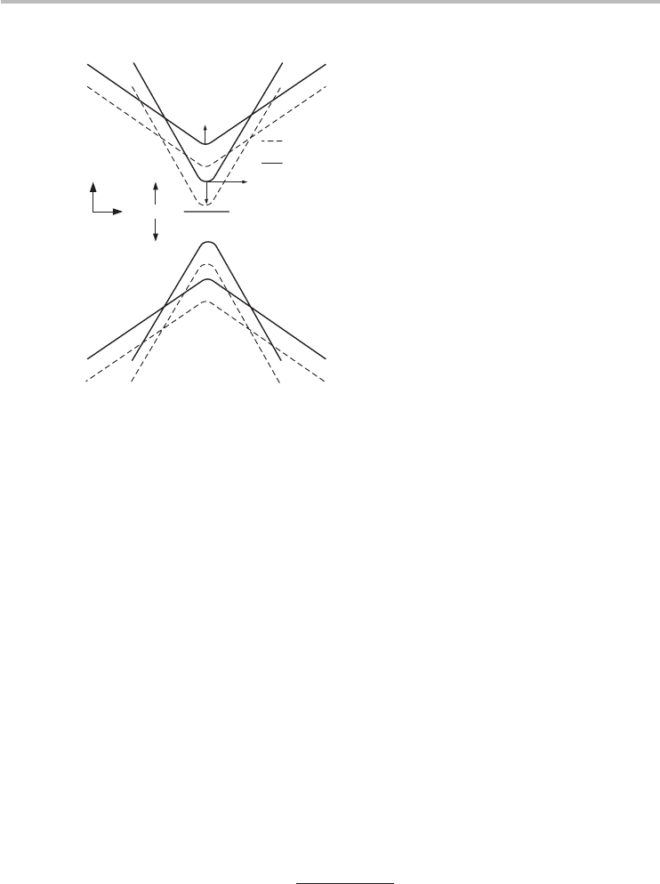
196 Chapter 8 Carbon nanotube field-effect transistors
E
F
E
cb
E
cb2
ϕ
S
V
G
> 0
V
G
= 0
E
k
E
g
Fig. 8.2 A simplified band structure including the first two subbands of semiconducting nanotubes.
E
cb2
is the energy minimum for the second subband. The effect of V
G
is to shift the bands
up (V
G
< 0) or down (V
G
> 0) with respect to the equilibrium Fermi energy, resulting in
a negative or positive ϕ
s
respectively.
respect to the equilibrium E
F
.
8
The polarity of the surface potential can be chosen
arbitrarily. We define the surface potential as positive if the bands move down and
negative if the bands move up with respect to their equilibrium position. This is
a convenient convention because it bestows the polarity of the gate voltage on
the surface potential. Furthermore, the polarity of ϕ
s
instantly reveals the majority
carrier in the nanotube:
ϕ
s
> 0, n-type CNT
ϕ
s
= 0, intrinsic CNT
ϕ
s
< 0, p-type CNT.
The surface potential is determined from the capacitive coupling of the gate to the
nanotube, as discussed in Chapter 6:
ϕ
s
=
C
ox
C
ox
+ C
q
(ϕ
s
)
V
G
= T
gc
V
G
, (8.1)
8
Indeed, it is not uncommon for some authors to use the concept of the chemical potential in a
virtually identical manner to surface potential. In that context, a positive V
G
moves E
F
up with
respect to a static band, which is the reverse of the ϕ
s
(see Figure 8.2), where the bands move
relative to E
F
. The departure of E
F
from its equilibrium value is the chemical potential. We use ϕ
s
to be consistent with conventional semiconductor transistor physics. In any case, the CNFET
device physics depend only on the energy difference between the subbands and E
F
, and both
approaches lead to the same results.

8.3 Surface potential 197
where V
G
is the gate voltage, C
q
is the CNT quantum capacitance per unit length,
and C
ox
is the electrostatic capacitance per unit length between the nanotube and
the gate metal, otherwise known as the oxide capacitance.
9
T
gc
is the gate coupling
transfer function. Equation (8.1) is a transcendental equation because the quantum
capacitance has an exponential dependence on ϕ
s
(seeChapter 6).Hence,ϕ
s
has to be computed numerically by self-consistent iteration in general. However,
for the purpose of obtaining insight into the nanotube device physics, a simple
analytical expression for the surface potential would be most welcome. Moreover,
an analytical expression would also be especially valuable in enabling compact
modeling of CNFET devices and CNFET device/circuit design.
To aid in deducing an approximate analytical form for ϕ
s
, it is worthwhile
investigating the quantum (C
q
<< C
ox
) and semiclassical (C
q
comparable to C
ox
)
capacitance limits seperately. At sufficiently low gate voltages there is relatively
smaller charge induced in the nanotube; hence, the CNFET will be in the quantum
capacitance limit with ϕ
s
≈ 1 and a unit slope (T
gc
= 1). At higher gate voltages,
both capacitances are comparable (semiclassical limit),and T
gc
becomes sub-linear
and less than unity. Mathematically, this is equivalent to
ϕ
s
≈
V
G
, C
q
C
ox
T
gc
V
G
, C
q
> C
ox
. (8.2)
Based on these insights, we can develop a phenomenological expression for the
gate coupling function given by the relation
T
gc
(V
G
) = 1 −
1 − T
gc,sc
(V
G
)
H
1 − T
gc,sc
(V
G
)
, (8.3)
where H (·) is the Heaviside step function and T
gc,sc
(V
G
) is an as-yet unknown
gate coupling function that should capture the sub-linear behavior in the semi-
classical limit. Observe that for T
gc,sc
(V
G
) = 1, T
gc
= 1, corresponding to the
quantum capacitance limit. The step function is simply employed as a convenient
mathematical tool to merge the solutions in the quantum and semiclassical limits
of operation. The challenge now lies in determining T
gc,sc
(V
G
). We recall from
Chapter 6 that the series combination of the quantum and oxide capacitances is
approximately linear with V
G
, at least over a restricted range. In that case, per-
haps a first-order Taylor series expansion might suffice. Specifically, we desire the
first-order series approximation of
T
gc,sc
=
C
ox
C
ox
+ C
q
(ϕ
s
)
. (8.4)
9
For CNT devices with both a top and bottom gate, C
ox
is expected to be the top-gate oxide
capacitance, because the bottom-gate oxide is often much thicker (by design) with lower dielectric
constant and, hence, has a relatively negligible influence on ϕ
s
. In general, a complete model of
such dual-gate devices should include the influence of both the top-gate and bottom-gate voltages.

198 Chapter 8 Carbon nanotube field-effect transistors
We will now explore a mathematical brute force technique exploiting the Taylor
series method in order to develop an analytical expression for the surface potential
that will capture the functional dependence on C
ox
, V
G
, temperature T , and the
CNT diameter or bandgap E
g
. Let us proceed by first focusing on electrons in
n-type devices (i.e., V
G
> 0), and subsequently the results will be extended to
holes in p-type devices. From Chapter 6, the electron quantum capacitance of a
semiconducting CNT (including only the first subband)
10
is
C
q
=
2e
2
N
o
e
x
n
#
1 + A e
(αx
n
+βx
2
n
)
(1 − α − 2βx
n
)
$
k
B
T
#
1 + A e
(αx
n
+βx
2
n
)
$
2
, x
n
=
2eϕ
s
− E
g
2k
B
T
, (8.5)
where A, α, and β are empirical constants in the analytical CNT carrier density
theory determined to be 0.63, 0.88, and 2.41 ×10
−3
respectively for temperatures
around 300 ± 100 K (see Eq. (5.66)). N
o
is the effective DOS:
N
o
=
8
a
E
g
+ k
B
T
E
g
+ 4γ
k
B
T
3πE
g
, (8.6)
where a is the graphene Bravais lattice constant (∼2.46 Å), γ is the nearest neigh-
bor overlap energy (∼3.1 eV), and k
B
is Boltzmann’s constant. To make Eq. (8.5)
significantly more manageable, we set α = 1 and β = 0, since their empirical values
are close to unity and zero respectively. These approximations are most welcome
for hand-analysis of the subsequent calculations and generally result in negligible
error in the low-energy regime. Of course, for a compact model using computa-
tional techniques, the approximations are unnecessary. With these approximations,
C
q
simplifies to
C
q
≈
2e
2
N
o
e
2eϕ
s
−E
g
2k
B
T
k
B
T
1 + A e
2eϕ
s
−E
g
2k
B
T
2
. (8.7)
The first-order Taylor series approximation of Eq. (8.4) about ϕ
s
= mE
g
results
in the following expression for the surface potential (in the semiclassical limit):
11
ϕ
s
= (c
0
− c
1
ϕ
s
)V
G
, (8.8)
10
Low-energy transport will be the primary focus of our exploration, and this is partly justified
because this regime offers the highest performance nanotube transistors. Moreover, the low
operating voltages in nanoscale technologies virtually guarantee that the low-energy regime is the
most relevant. In this regime, electrons in the first subband dominate the electrostatic properties.
11
The first-order Taylor series expansion of C
ox
/(C
ox
+ C
q
) = 1/[1 +(C
q
/C
ox
)] yields the
binomial approximation 1/(1 +x) ∼ 1 − x, which is increasingly accurate as x becomes much
smaller than unity.