Wong H.-S.P., Akinwande D. Carbon Nanotube and Graphene Device Physics
Подождите немного. Документ загружается.


8.6 Ballistic CNFET performance parameters 209
(ii) Partially ballistic transport: This is defined as transport with no acoustic
phonon scattering but possibly some optical phonon scattering (α<1).
The DOPS effect is expected to apply to ballistic FETs in general, including
silicon FETs.
22
Further research is warranted to investigate how the DOPS param-
eter scales with the device dimensions and semiconductor-contact dynamics, with
the potential that the results of such investigations might lead to optimizing the
device to minimize this effect. In the next section we will discuss and enumerate
the performance parameters of the ballistic CNFET.
8.6 Ballistic CNFET performance parameters
Many of the basic parameters that characterize transistor performance can now
be derived from the experimentally validated ballistic theory. This includes fun-
damental parameters such as the threshold voltage V
T
, the transconductance
(g
m
= ∂I
D
/∂V
G
), and the channel conductance (g
ds
= ∂I
D
/∂V
D
). In addition, the
sub-threshold current I
sth
and associated slope and the saturation or ON current
I
ON
are of routine interest.
The threshold voltage for an FET is defined as the gate voltage at which a
sufficient amount of carriers are induced to create a conducting channel. Strictly
speaking, in silicon FETs, V
T
corresponds to the gate voltage where an inversion
layer is induced at the interface between the gate oxide and the silicon substrate.
23
For an intrinsic semiconductor, the threshold voltage takes on a somewhat vague
meaning because of the lack of carrier inversion, as is the case in conventional
doped semiconductors. To circumvent this ambiguity, we can define a threshold
voltage that does not rely on carrier inversion yet still have virtually the same prop-
erties characteristic of V
T
in conventional FETs. Mathematically, we define V
T
to
be the gate voltage at which the gradient of the transconductance is a maximum, as
shown in Figure 8.9a.
24
This definition is universally applicable to all CNFETs and
in general to all FETs based on an intrinsic semiconductor channel. Moreover, the
defined V
T
can be directly determined from experimental measurements, avoiding
altogether the extraction ambiguities related to small-dimensional effects in the
conventional definition of V
T
.
22
K. Natori, Ballistic MOSFET reproduces current-voltage characteristics of an experimental
device. IEEE Electron Device Lett., 23 (2002) 655–7.
23
For example, the channel of a silicon n-FET is normally doped with holes; therefore, a
non-conducting path exists between the electron-doped S/D regions and the channel. To turn ON
the device, a positive gate voltage exceeding V
T
has to be applied to invert the channel from
p-type to n-type, leading to the creation of a conducting path.
24
This definition has been previously introduced for thin-oxide FETs. See H.-S. Wong, M H. White,
T. J. Krutsick and R. V. Booth, Modeling of transconductance degradation and extraction of
threshold voltage in thin oxide MOSFETs. Solid-State Electron., 30 (1987) 953–68.
210 Chapter 8 Carbon nanotube field-effect transistors
(a) (b)
0.1
0.2
0.3
0.4
0.5
1 1.5 2 2.5 3
CNT diameter(nm)
Threshold voltage (V)
aV
D
= 0.05
V
D
= 0.8
V
G
(V)
g
m,
∂
gm
/∂V
G
(arb.units)
∂g
m
/∂V
G
g
m
V
T
2d
t
1
Fig. 8.9
(a) The graphical illustration of the definition of V
T
for CNFETs with an intrinsic channel.
(b) V
T
exactly computed from the analytical ballistic theory model for a ballistic 50 nm
n-type CNFET (derived from Figure 8.4) showing weak dependence on drain voltage and
a simple ∼0.5/d
t
relation.
Forann-CNFET,thethresholdvoltageisapproximatelygivenby
14
V
T
≈ k
B
T ln
1
12
e
(E
g
+eαV
D
)/2k
B
T
#
24 + e
(eαV
D
)/k
B
T
− e
(eαV
D
)/2k
B
T
$
,
(8.29)
which can be further simplified (via a first-order Taylor series expansion) to reveal
a relationship that is directly proportional to the bandgap and, hence, inversely
proportional to the nanotube diameter (since E
g
∼ 1/d
t
):
eV
T
≈
1
2
E
g
+ offset. (8.30)
This relationship is confirmedin Figure 8.9b (where theoffset is simply set tozero),
showing the V
T
computed exactly from the ballistic model compared with a simple
V
T
∼ 0.5/d
t
(V nm) relation with good agreement. A suite of analytical formulas
for basic transistor performance parameters are shown in Table 8.2, which the
reader is strongly encouraged to derive for intellectual satisfaction. The parameters
are easily derivable using elementary algebra and calculus. The sub-threshold
current is the current when V
G
< V
T
and is an increasingly important parameter
relevant to power dissipation and gate control in nanoscale electronics. Techniques
to extract the DOPS parameter and the bandgap or the flatband voltage are also
enumerated in the table.
Much of the excitement about CNFETs concerns their potential performance
advantages over silicon transistors for nanoscale digital, analog, and radio-
frequency (RF) applications. For this reason, several workers have benchmarked
the performance of relatively ideal CNFETs to silicon FETs, and the consensus out-
look is that, qualitatively speaking, ballistic CNFETs offer superior performance to
8.6 Ballistic CNFET performance parameters 211
Table 8.2. Expressions for the key metrics of CNFETs and some parameter extraction techniques
# Analytical equations for ballistic n-type CNFET Comments/conditions
(1) I
ON
≈
k
B
T
eR
q
ln
#
1 +e
(2eϕ
s
−E
g
)/2k
B
T
$
Saturation current in
active region (V
G
>
V
T
, V
D
> V
G
− V
T
)
(2) I
sth
≈
k
B
T
eR
q
#
e
(2eV
G
−E
g
)/2k
B
T
− e
(2eV
G
−2αeV
D
−E
g
,2k
B
T
$
Sub-threshold current
with an ideal slope of
60 mV/decade at 300 K
(V
G
< V
T
)
(3) V
G
= V
T
, when
∂g
m
∂V
G
= maximum Definition for V
T
for
intrinsic CNFETs
(4) V
T
≈ k
B
T ln
1
12
e
(E
g
+αeV
D
)/2k
B
T
#
√
e
(αeV
D
)/k
B
T
+ 24 − e
(αeV
D
)/2k
B
T
$
Analytical V
T
in the limit
of ϕ
s
∼ V
G
(5) g
m
=
∂I
D
∂V
G
=
1
1 +e
(2eϕ
3
−2αeV
D
−E
g
)/2k
B
T
−
1
1 +e
(2eϕ
3
−E
g
)/2k
B
T
1
R
q
∂ϕ
s
∂V
G
Transconductance
(6) g
ds
=
∂I
D
∂V
D
=
α
R
q
#
1 +e
(E
g
+2αeV
D
−2eϕ
s
)/2k
B
T
$
−1
Channel conductance
(7) g
ds0
=
α
R
q
Technique to extract α
from g
ds
(V
D
→ 0,
V
G
→ V
DD
)
(8) 2k
B
T ln
eR
q
k
B
T
I
sth
= 2e(V
G
− V
FB
) −E
g
Technique to extract E
g
or
V
FB
from measured
I
sth
(V
D
→ V
DD
)
siliconFETsforcomparablechannellengthsandelectricalconditions.
14,15,25
The
actual quantitative performance advantage depends on the modeling details and
associated approximations. However, contemporary CNFETs that are frequently
fabricated do not represent the ideal ballistic CNFET; and, furthermore, any perfor-
mance benefits begin to diminish when parasitic capacitances are included in the
device geometry.
26
At this moment, significant advances are required to routinely
fabricate near-ideal nanotube FETs to realize their intrinsic electrical performance.
25
J. Guo, S. Hasan, A. Javey, G. Bosman and M. Lundstrom, Assessment of high-frequency
performance potential of carbon nanotube transistors. IEEE Trans. Nanotechnol., 4 (2005)
715–21; L. Wei, D. J. Frank, L. Chang and H.-S. P. Wong, A non-iterative compact model for
carbon nanotube FETs incorporating source exhaustion effects. IEEE IEDM Tech. Digest, (2009)
917–20.
26
N. Patil, J. Deng, S. Mitra and H.-S. P. Wong, Circuit-level performance benchmarking and
scalability analysis of carbon nanotube transistor circuits. IEEE Trans. Nanotechnol., 8 (2009)
37–45.

212 Chapter 8 Carbon nanotube field-effect transistors
8.7 Quantum CNFETs
Carbon nanotube FETs can exhibit very novel properties when working in the
quantum capacitance limit, particularly in the active region of transistor operation.
These novel properties, as we shall see shortly, are quite unique and not observable
in conventional semiconductor FETs that possess a large DOS (such as silicon).
For brevity, we refer to a CNFET that satisfies the quantum capacitance limit in
all its regions of operation (sub-threshold, linear, and active) as a quantum FETs
in order to distinguish its unique properties from the conventional or classical
FET. The quantum capacitance limit entails that C
ox
C
q
, and hence ϕ
s
≈ V
G
.
Accordingly, the gate has maximum control of the electrical properties of the
channel in a quantum CNFET.
To actually realize a quantum CNFET requires that the oxide capacitance be
much greater, say about an order of magnitude greater, than the quantum capaci-
tance. It is worthwhile obtaining an estimate of the oxide capacitance to satisfy this
requirement. Continuing with our focus on low energies (i.e. only the first subband
is considered), the maximum C
q
of semiconducting nanotubes is about a factor of
2 greater than the quantum capacitance of metallic nanotubes. That is, maximum
C
q
≈ 0.6 fF µm
−1
(see Chapter 6); therefore, C
ox
needs to be >6fFµm
−1
.
27
Substituting ϕ
s
= V
G
into Eq. (8.28), the I −V expression of a quantum CNFET is
I
D
= I
o
%
ln
#
1 + e
(±2eV
G
−E
g
)/2k
B
T
$
− ln
#
1 + e
(±2eV
G
∓2eαV
D
−E
g
)/2k
B
T
$&
.
(8.31)
Consider the saturation current (say for an n-CNFET) given by
I
ON
= I
o
ln
#
1 + e
(2eV
G
−E
g
)/2k
B
T
$
≈
V
G
R
q
−
E
g
2eR
q
, (8.32)
where the approximation is valid for typical gate voltages and bandgaps. For
example, a CNT with a bandgap ∼0.6 eV has a threshold voltage of ∼0.3 V under
flatband conditions. At room temperature, for V
G
> 0.35 V, the exponential term
is ∼ 54.6 1. Since the current is linear with voltage, the transconductance is a
constant:
g
m
≈
1
R
q
(8.33)
27
In principle, this can be realized by a 10 nm thin dielectric with k > 350. However, at present, it
is not at all certain that this value of oxide capacitance on a CNT is achievable. Most higher k
metal oxides, such as various types of titanates, have a thickness-dependent k which can exceed
1000 for thick films, but often drops below 200 for t
ox
< 50 nm. At the same time, such higher k
dielectrics have the undesirable effect of preferentially screening the drain field through the
dielectric. See D. Frank et al. in footnote 35.
8.8 Schottky-barrier ballistic CNFETs 213
0 2 0.4 0.6 0.8 1
25
50
75
100
125
150
175
154.2
25 50 75 100
T (°C)
125 150 175 200
154.4
154.6
154.8
155
V
GS
(V)
g
m
(µS)
g
m
(µS)
(a)
(b)
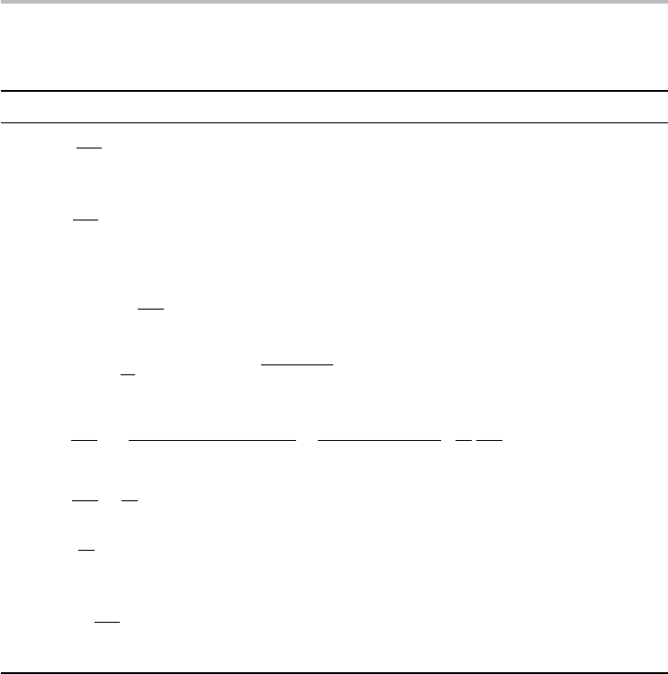
Fig. 8.10 Novel and highly desirable properties of the quantum CNFET. (a) The transconductance
dependence on V
G
revealing a flat response in the active region over a wide range of
voltages (at 300 K). (b) Temperature profile of g
m
, showing less than 1 % variation up to
150
◦
C. For this example, E
g
= 0.5 eV, V
D
= 1V,V
G
= V
D
/2, and α = 0.5.
This is a remarkable result in contrast with conventional FETs, where the
transconductance in the active region can generally be expressed as a power series
function of the small-signal gate voltage in the form g
m
≈ a
o
+a
1
v
g
+a
2
v
2
g
+···,
where v
g
is the small-signal gate voltage.The constant transconductance of a quan-
tum CNFET is actually preferable, particularly for analog and RF circuits, where
much effort is often devoted to suppressing the gate dependence of the transcon-
ductance in classical FETs that inevitably leads to signal distortion at large signal
amplitudes.
28
In addition, the transconductance of the quantum CNFET also con-
tains no explicit dependence on temperature, a property which is highly desirable
in analog/RF circuits. The actual state of affairs regarding the transconductance
profile of a quantum CNFET is shown in Figure 8.10. For this example, we have
employed the actual I−V expression in Eq. (8.31) to get an accurate outlook on
the profile of g
m
. The roll-off of the transconductance at higher gate voltages is
because the semiconducting CNT is becoming more metallic-like.
8.8 Schottky-barrier ballistic CNFETs
Carbon nanotube FETs with Schottky (source/drain) metal contacts are frequently
the type of CNFETs commonly encountered in practice not by intention or design,
but simply because it is far easier to obtain Schottky contacts to semiconduct-
ing nanotubes instead of the more desirable ohmic kind. This is because it takes
a great deal more diligent effort to engineer the metal–nanotube interface to be
28
Common circuit techniques include ratiometric circuits and feedback or feedforward circuits. For
an insightful discussion of distortion and linearity in analog/RF integrated circuits, see T. H. Lee,
The Design of CMOS Radio-Frequency Integrated Circuits, 2nd edn (Cambridge University
Press, 2004) Chapter 12.

214 Chapter 8 Carbon nanotube field-effect transistors
transparent to charge carriers. Moreover, routine fabrication process conditions
appear to conspire to favor Schottky barriers more often than not.
29
As a result, it
is important to understand the device physics and I −V characteristics of Schottky-
barrier CNFETs. A welcome bonus from this endeavor is that the understanding
gained deeply broadens our intuition about Schottky-barrier nanoscale transistors
in general, including CNR transistorsand semiconductor nanowire transistors.And
in fact, understanding of Schottky-barrier device physics is necessary to under-
stand (undesired) leakage current and the implications for ON/OFF current ratio
in (metal) ohmic-contact ballistic CNFETs and similar 1D ballistic FETs, as will
become evident in the course of the narrative.
The presence of Schottky barriers introduces substantial complexity in describ-
ing charge transport in the nanotube transistor owing to the inherently rich device
physics. As such, it is quite easy to get lost or lose focus of the central device
physics. This is especially true for the beginning student reader in this subject
matter. For this reason, the discussion will be more of a gentle and simple intro-
duction to Schottky-barrier nanotube transistors, with primary coverage of the
basic transistor physics and the current–voltage characteristics. References will be
provided along the way for advanced studies.
We begin our studies of Schottky-barrier CNFETs by exploring the bias-
dependent band diagrams in order to obtain basic qualitative insight about charge
transport. The use of band diagrams is essential in understanding and discussing
charge dynamics in these transistors. For convenience, we focus our attention on an
n-type transistor operation in the ballistic regime with a mid-gap Schottky barrier
and zero flatband voltage,
30
conditions which are much easier to handle analyti-
cally and still provide us with the wealth of basic insights that are usually valid
and can be adapted to explain charge transport under general conditions.
Figure 8.11 illustrates the band diagrams under different bias conditions, where
the primary role of the gate voltage is to modulate the barrier thickness for electron
tunneling, and the role of the (positive) drain voltage is to rigidly lower the barrier
height at the drain electrode. The basic ideas regarding ballistic transport in ohmic-
contact CNFETs apply here with the additional effects of quantum mechanical tun-
neling that must be properly accounted for. In a sense, the transistor can be consid-
ered as two Schottky barriers connected by a field-free region in the channel of the
nanotube.We considerlow-energy transport, whichincludes only the firstsubband.
Different bias conditions applied to the transistor can produce a diversity of
charge transport phenomena, including source and drain electron tunneling in the
29
Indeed, a search of published experimental nanotube transistors in one’s favorite journals will
unambiguously show that the vast majority (but not all) of CNFETs fabricated under different
permutations of metal contacts, process conditions, and nanotube diameters produce
Schottky-barrier CNFETs. Intuitively, metal workfunction and process and ambient conditions all
play a role, but the degree of their influence in experimental devices remains unclear.
30
In optimized device designs, the gate metal (and associated workfunction) is carefully selected to
set the flatband voltage and, hence, the threshold voltage. The metal contacts are also chosen
diligently to control the Schottky-barrier height.
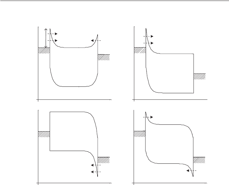
8.8 Schottky-barrier ballistic CNFETs 215
(a) (b)
ϕ
be
x
V
G
> V
t
E
E
F
x
V
D
= V
G
> V
T
E
E
F
x
V
G
= V
D
/2
E
E
F
x
E
E
F
E
F
– eV
D
E
F
– eV
D
E
F
– eV
D
E
F
– eV
D
V
G
=0, V
D
> V
T
(c) (d)
Fig. 8.11 Band diagrams of a ballistic n-CNFET with a mid-gap Schottky barrier under selected
bias conditions (ϕ
be
is the Schottky barrier height for electrons). (a) Band diagram in the
linear region. The net current is the difference between electrons tunneling from the
source and those tunneling from the drain. (b) The transistor ON state, where current is
supplied from electrons tunneling from the source. (c) Band diagram in the OFF state.
Note the valence band symmetry with the conduction band of (b). As a result, the current
from holes tunneling from the drain will be identical to electron current in (b) for the same
V
D
. (d) Interesting bias conditions leading to symmetrical conduction and valence band
profile and, hence, equal electron and hole currents.
linear region (Figure 8.11a) and electron source tunneling in the active or ON
region (Figure 8.11b). Intriguingly, we discover it is difficult to turn off the tran-
sistor (OFF bias is conventionally defined as V
G
= 0 V, and V
D
= V
DD
). In fact,
for the device conditions under examination (V
FB
= 0 V, and a mid-gap Schottky
barrier), at V
G
= 0 V, hole tunneling from the drain to the source results in current
that is equal to the ON current when V
G
= V
D
. This instantly implies that the
Schottky-barrier CNFET is fundamentally an ambipolar transistor, with electrons
providing the bulk of the current above a critical gate voltage and holes respon-
sible for the current below the critical V
G
.
31
On deeper thought, we expect the
31
These conclusions continue to hold for arbitrary Schottky-barrier heights, even including the
special case of a vanishing ϕ
bn
(a CNFET with transparent contacts which was the subject of
previous sections). The effect of arbitrary Schottky-barrier heights is primarily to modify the
magnitude of the ON and OFF currents and shift the position of the critical V
G
. The overall
216 Chapter 8 Carbon nanotube field-effect transistors
~e
-x/ λ
0
–eV
D
x
E
E
cb
E
cb
– eV
D
E
cb
- ew
s
source/drain tunneling
source tunneling
Γ
s
Γ
d
thermionic emission
T
s
T
d
T
s
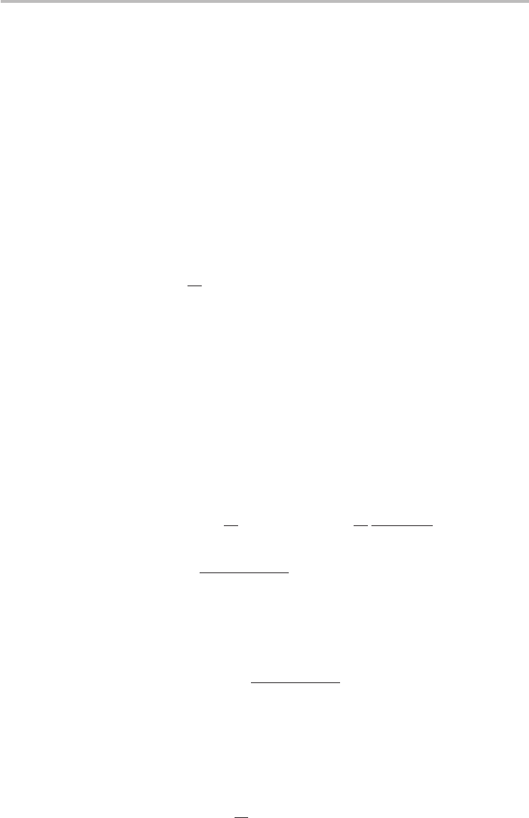
Fig. 8.12 The conduction band profile of a Schottky-barrier CNFET showing the source/drain
tunneling and reflection processes and the thermionic component of current from
high-energy electrons. E
F
= 0 eV for reference.
critical gate voltage to correspond to the case when the electron and hole currents
must be equal. Indeed, we can construct a band diagram that is consistent with this
electron–hole current symmetry, as shown in Figure 8.11d, where the critical gate
voltage or symmetry point is determined to be V
G
= V
D
/2. With these qualitative
insights it is possible to forecast the general I
D
−V
G
profile of the Schottky-barrier
CNFET without actually writing a single equation. In the OFF state, hole tunnel-
ing produces substantial current, which reduces as V
G
increases. At the symmetry
point, electron tunneling equals hole tunneling and the current in the transistor
is at a finite minimum. For further increases in V
G
, electron tunneling provides
increasing current, which reaches a maximum at V
G
= V
D
. Stated differently, for
a fixed V
D
, the hole current increases with V
D
−V
G
in exactly the same manner as
the electron current increases with V
G
.All in all, a sketch of the I
D
−V
G
is expected
to more or less reveal a V-shaped profile.
A quantitative semi-analytical model of transport in Schottky-barrier CNFETs
that is especially beneficial for nurturing intuition can be developed by employ-
ing the Landauer–Büttiker formalism where the Schottky barriers are treated as
scattering sites near the contacts.
32
Inside the channel, transport is ballistic and
ambipolar nature is still preserved. See J. Guo, S. Datta and M. Lundstrom, A numerical study of
scaling issues for Schottky-barrier carbon nanotube transistors. IEEE Trans. Electron Devices, 51
(2004) 172–7. Note that, in CNFETs with a finite V
FB
, the ambipolar feature may not be visible
within a limited gate voltage sweep, but inevitably becomes observable for a larger range.
32
The theory of Schottky-barrier CNFETs often involves a set of assumptions and approximations.
In the present treatment, our goal is to create a simple physics-based model that predicts the
correct qualitative features while retaining reasonable accuracy.

8.8 Schottky-barrier ballistic CNFETs 217
equilibrium conditions apply. The contact themselves are considered to be reser-
voirs of electrons at (or near) thermal equilibrium and, hence, the use of the
equilibrium Fermi–Dirac distribution is valid. Furthermore, we consider only the
case where the mobile electrons have arbitrary or random phase. For this reason,
constructive or destructive interference from multiple coherent scattering at the
two tunneling barriers, which can lead to resonant tunneling phenomena,
33
can
be neglected in the CNFET model. The neglect of interference is reasonable for
currently achievable short channel lengths (tens of nanometers). However, at much
shorter channel lengths roughly comparable to the thickness of the tunnel barriers,
resonant tunneling effects become increasingly important.
We develop the Schottky-barrier CNFET model in simple stages of increas-
ing detail, in line with the gentle introduction which is our driving philosophy.
First, we state the formula for the Schottky-barrier ballistic current, then eluci-
date on the effective tunneling probabilities of mobile charges, and finally we will
focus on developing an analytical expression for the tunneling probabilities appli-
cable to CNFETs. This modeling strategy offers a seamless transition between
Schottky-barrier CNFETs and ohmic-contact CNFETs discussed in the previous
sections. The electron current I
e
can be expressed following the Landauer–Büttiker
formalism,
34
I
e
=
4e
h
∞
E
cb
−eϕ
s
[
T
sd
(E)F(E, E
F
) − T
ds
(E)F(E, E
F
− eV
D
)
]
dE (8.34)
where T
sd
is the source to drain transmission probability or coefficient of an
electron-wave propagating from the source to the drain, successfully through both
Schottky barriers, and vice versa for T
ds
. This expression essentially has the same
form has the previously discussed ballistic current integral, Eq. (8.21), but mod-
ified by the transmission probabilities. The transistor drain current is the sum of
the electron and hole currents. We will explore the electron current for now in
order to develop expressions for the tunneling probabilities; subsequently, it is a
straightforward matter to write the expression for the hole current.
Let us consider an electron already in the channel, propagating to the drain.
The pressing question is: What is the transmission probability of this electron
propagating to the drain reservoir? Let us call this channel to drain transmission
probability T
cd
. Furthermore, electrons that do not tunnel through the barrier are
reflected backwards. We can label the transmission and reflection coefficients at
the source and drain as T
s
,
s
and T
d
,
d
respectively (see Figure 8.12). It follows
33
J. Singh, Quantum Mechanics: Fundamentals & Applications to Technology (John Wiley, 1997).
34
S. Datta, Electronic Transport in Mesoscopic Systems (Cambridge University Press, 1995).
218 Chapter 8 Carbon nanotube field-effect transistors
that T
cd
is a sequential sum of a series of scattering events:
T
cd
= T
d
+
d
s
T
d
+ (
d
s
)
2
T
d
+ (
d
s
)
3
T
d
+···+(
d
s
)
n
T
d
,
T
cd
= T
d
1 +
n
i
(
d
s
)
i
. (8.35)
Likewise, the total probability that the electron will be reflected into the source
reservoir
cs
is a sum of events:
cs
=
d
T
s
+
2
d
s
T
s
+
3
d
2
s
T
s
+···+
n
d
n−1
s
T
s
,
cs
=
T
s
s
n
i
(
d
s
)
i
. (8.36)
Owing to charge conservation (i.e. the electron can be found either at the source
or drain with a certain probability), the transmission and reflection coefficients are
related by
T
cd
+
cs
= 1. (8.37)
Substituting Eq. (8.36) for
cs
, the channel to drain transmission probability in
terms of T
s
and T
d
simplifies to
T
cd
= 1 −
T
s
s
n
i
(
d
s
)
i
= 1 −
T
s
s
(T
cd
− T
d
)
T
d
,
T
cd
=
T
d
T
s
+ T
d
− T
s
T
d
. (8.38)
Therefore, it follows that the source to drain transmission probability is T
cd
multiplied by the source transmission probability:
T
sd
=
T
s
T
d
T
s
+ T
d
− T
s
T
d
= T
eff
. (8.39)
Note that the symmetry involving T
s
and T
d
in the expression immediately implies
that T
ds
= T
sd
. To retain this symmetry in the symbolic notation, T
eff
will be used
hereafter. The electron current can now be stated as
I
e
=
4e
h
∞
E
cb
−eϕ
s
T
eff
(F
s
− F
d
)dE, (8.40)