Wong H.-S.P., Akinwande D. Carbon Nanotube and Graphene Device Physics
Подождите немного. Документ загружается.


8.8 Schottky-barrier ballistic CNFETs 219
where the shorthand F
s
and F
d
are used to represent the Fermi–Dirac distribution
at the source and drain respectively. Similarly, the hole current is given by
I
h
=
4e
h
−∞
−E
cb
−eϕ
s
T
eff
(F
d
− F
s
)dE. (8.41)
The total drain current is I
D
= I
e
+ I
h
.
We can now go one step further and expand I
e
for the usual operating biases of
an n-CNFET (V
G
≥ 0, V
D
≥ 0) regardless of the specific form of T
eff
in order to
demonstrate how the limits of the integral need to be handled. Since the Schottky
barrier only exists for a finite range of electron energies, the restrictions on the
allowed values of the source transmission probabilities are (see Figure 8.12 for
visual illustration)
E ≤ E
cb
− eϕ
s
, T
s
= 0 (electrons below the bottom of the band have
no states to tunnel into);
E
cb
− eϕ
s
< E < E
cb
, T
s
= T
s
(E)(the energy range where the
Schottky-barrier exists);
E ≥ E
cb
, T
s
= 1 (thermionic emission of high-energy electrons
above the barrier).
Similarly, the drain transmission probabilities must satisfy the following restric-
tions when E
cb
− eϕ
s
< E
cb
− eV
D
:
E ≤ E
cb
− eϕ
s
, T
d
= 0;
E
cb
− eϕ
s
< E < E
cb
− eV
D
, T
d
= T
d
(E);
E ≥ E
cb
− eV
D
, T
d
= 1,
otherwise, when E
cb
−eϕ
s
≥ E
cb
−eV
D
, T
d
= 1, because the Schottky barrier no
longer exists at the drain contact.
For E
cb
− eϕ
s
< E
cb
− eV
D
, the electron current can be expanded into three
integrals:
I
e
=
4e
h
E
cb
−eV
D
E
cb
−eϕ
s
T
eff
(F
s
− F
d
)dE
(
)* +
both barriers present
+
E
cb
E
cb
−eV
D
T
s
(F
s
− F
d
)dE
( )* +
only source barrier
present
+
∞
E
cb
(F
s
− F
d
)dE
( )* +
thermionic
emission
,
(8.42)

220 Chapter 8 Carbon nanotube field-effect transistors
while for E
cb
− eϕ
s
≥ E
cb
− eV
D
, the electron current is
I
e
=
4e
h
E
cb
E
cb
−eϕ
s
T
s
(F
s
− F
d
) dE +
∞
E
cb
(F
s
− F
d
) dE
. (8.43)
The key point from this exercise is the need to handle the limits of the integral(s)
thoughtfully to reflect the changing existence of the Schottky barriers.
In order to quantify the impact or effect of the Schottky barriers in reducing
the current when the transistor is ON, we can introduce a dimensionless metric
appropriately termed the Schottky-barrier impact (SBI) factor ! defined as
!(V
G,D
= V
DD
) =
I
D,Ohmic
− I
D,SB
I
D,Ohmic
=
E
cb
E
cb
−eϕ
s
(1 − T
s
)(F
s
− F
d
) dE
∞
E
cb
−eϕ
s
(F
s
− F
d
) dE
, (8.44)
where I
D,Ohmic
is the ballistic current in a CNFET with transparent contacts and
I
D,SB
is the corresponding current in the presence of Schottky barriers. Note that,
in the ON state, the electron current given by Eq. (8.43) should be used for I
D,SB
.
For values of ! approaching unity, the Schottky barrier has minimal impact on
the ON current, while for ! → 0, the Schottky barrier substantially degrades the
ON current. If Schottky barriers are inevitable in a particular FET, to the goal is
to engineer the barriers so as to achieve ! values close to unity.
The final part of the analysis is to model the tunneling of electrons through the
Schottky barriers with the aim of obtaining an analytical expression for T
s
and
T
d
. The position-dependent energy band potential profile for mid-gap Schottky
barriers (see Figure 8.12) can be modeled with exponential functions to first order,
described by
E
c
(x) = E
cb
+ eϕ
s
#
e
−x/λ
+ e
(x−L)/λ
− e
−L/λ
− 1
$
+ eV
D
#
e
−L/λ
− e
(x−L)/λ
$
,0≤ x ≤ L, (8.45)
E
v
(x) = E
c
(x) − E
g
, (8.46)
where E
c
and E
v
are the position-dependent conduction band minima and valence
band maxima respectively and L is the channel length. The reader is welcome
to show that the expressions for the potential profiles are indeed valid given
that the reference (zero) potential is the source E
F
. λ is a length scale on which
potential variations occur; in other words, a measure of the Schottky barrier thick-
ness. The concept of λ is rooted in evanescent-mode analysis, which in essence
decouples the vertical electrical field from the horizontal field and enables simple

8.8 Schottky-barrier ballistic CNFETs 221
exponential expressions for the potential variation.
35
An accurate theory for λ has
yet to be developed for CNFETs; however, some analysis has revealed that it is
proportional and comparable to the oxide thickness.
36
In the meantime, it can be
considered a phenomenological fitting parameter until further research produces
an experimentally verifiable theory.
An analytical expression for the transmission probabilities is achievable within
the Wentzel–Kramers–Brillouin (WKB) approximation by means of the potential
profile expressions and the effective mass theorem, which considers the low-energy
mobile electrons as free electrons with an effective mass m
∗
that accounts for
their solid-state environment. The details of the WKB approximation are deferred
to the many introductory quantum-mechanical textbooks that provide rigorous
treatment.
33
The effective-mass approximation is likely the weakest assumption so
far. Fortunately, published analysis suggests that the effective-mass approximation
is reasonably accurate for tunneling in carbon-based transistors with Schottky
barrier heights less than ∼0.5 eV.
37
For mid-gap Schottky barriers this will include
nanotubes with bandgaps up to ∼1 eV (down to d
t
∼ 0.9 nm). The primary benefit
of the effective-mass approximation within the WKB formalism is the inherent
simplicity and the accessible qualitative insights. With this in mind, the WKB
formulas for the transmission probabilities are (subject to the energy restrictions
stated previously)
ln(T
s
(E)) =−
4λ
√
2m
∗
E
cb
− E −
E − (E
cb
− eϕ
s
) tan
−1
E
cb
− E
E − (E
cb
− eϕ
s
)
,
(8.47)
ln(T
d
(E)) =−
4λ
√
2m
∗
×
E
cb
− eV
D
− E −
E − (E
cb
− eϕ
s
) tan
−1
E
cb
− eV
D
− E
E − (E
cb
− eϕ
s
)
.
(8.48)
In general, the transmission probabilities have a quasi-exponential dependence on
energy, with values approaching unity for tunneling electrons close to the top of
the Schottky barrier. These formulas are valid for an n-CNFET with an equilibrium
mid-gap Schottky barrier under normal operating bias conditions (V
G
, V
D
≥ 0).
For p-CNFETs, and arbitrary Schottky barrier heights, the formulas can be adapted
35
For in-depth discussions regarding λ, see D. J. Frank, Y. Taur and H.-S. P. Wong, Generalized
scale length for two-dimensional effects in MOSFETs. Electron Device Lett., 19 (1998) 385–7;
and S. H. Oh, D. Monroe and J. M. Hergenrother, Analytic description of short-channel effects in
fully-depleted double-gate and cylindrical, surrounding-gate MOSFETs. IEEE Electron Device
Lett., 21 (2000) 443–7.
36
A. Hazeghi, T. Krishnamohan and H.-S. P. Wong, Schottky-barrier carbon nanotube field-effect
transistor modeling. IEEE Trans. Electron Devices, 54 (2007) 439–45.
37
P. Michetti and G. Iannaccone, Analytical model of 1D carbon-based Schottky-barrier transistors.
IEEE Trans. Electron Devices, 57 (2010) 1616–25.
222 Chapter 8 Carbon nanotube field-effect transistors
(a)
0 0.1 0.2 0.3 0.4 0.5 0.6
10
–4
10
–3
10
–2
10
–2
10
–1
10
0
10
1
10
–1
10
0
10
1
I
D
(
µ
A)
V
GS
(V)
V
G
(V)
ϕ
be
= E
g
/2
ϕ
be
= 0
V
D
= 0.4 V
(b)
0 0.1 0.2 0.3 0.4 0.5 0.6
I
D
(µA)
λ = 3 nm
λ = 2 nm
λ = 1 nm
V
D
= 0.4 V
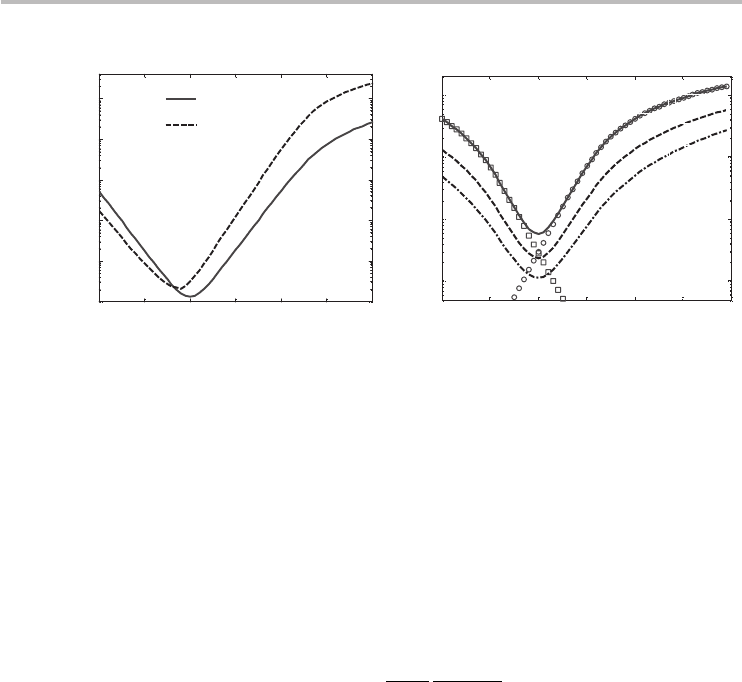
Fig. 8.13 n-CNFET characteristics. (a) I
D
−V
G
with transparent contacts (ϕ
be
= 0) and mid-gap
Schottky barriers (ϕ
be
= E
g
/2). Ambipolar characteristics exist in both cases. d
t
∼ 1nm
(E
g
∼ 0.9 eV), and λ ∼ 1.1 nm, corresponding to a thin gate oxide (say <5 nm). (b) The
consequences of increased Schottky-barrier thickness (∼λ). Increasing λ reduces the ON
current (approximately) exponentially and also degrades the sub-threshold slope. For this
example, λ = 1 nm, 2 nm, and 3 nm results in sub-threshold slopes of ∼70 mV/decade,
∼82 mV/decade, and ∼100 mV/decade respectively. For λ = 1 nm, the open circles and
squares are the electron and hole current contributions respectively. d
t
∼ 1.5 nm.
in a straightforward manner. The band-minima effective mass was derived in
Chapter 5 and is recalled here for convenience:
m
∗
=
4
2
3γ a
2
E
g
2γ + E
g
(8.49)
where the band structure constants γ and a are numerically ∼3.1 eV and ∼2.46 Å
respectively.
Figure 8.13 is a graph of the characteristic I −V profile of Schottky-barrier
ballistic CNFETs revealing ambipolar transport. The minimum current occurs at
V
G
= V
D
/2,
38
and corresponds to the band diagram of Figure 8.11d, as previously
noted. Likewise, charge transport corresponding to V
G
= V
D
and V
G
= 0V
can also be explained visually by Figure 8.11b and Figure 8.11c respectively.
The Schottky barriers usually reduce and limit the ON current compared with
an identical CNFET with transparent contacts. Moreover, thicker barriers result
in significant current reduction and degraded sub-threshold slope. Likewise, the
transistor conductance also suffers from thicker barriers (i.e. thicker oxides) or
tallerbarriers.
36
Fromanapplicationpointofview,thesubstantialOFFcurrent
is generally unacceptable; hence, in practice, gate workfunction engineering is
38
This bias point is actually the optimum point for electron–hole recombination which produces
maximum optical emission. See J. A. Misewich, R. Martel, Ph. Avouris, J. C. Tsang, S. Heinze
and J. Tersoff, Electrically induced optical emission from a carbon nanotube FET. Science, 300
(2003) 783–6.

8.9 Unipolar CNFETs 223
required to produce the necessary flatband voltage that shifts the I−V curve to
the left such that the minimum current is ideally at V
G
= 0 V. For completeness,
we note that decreasing the bandgap for a fixed V
D
or increasing V
D
(or the drain
power supply) for a fixed bandgap results in appreciably greater increase in the
minimum current than in the ON current; consequently, the ON/OFF current ratio
is significantly compromised.
39
To sum up, the non-trivial challenges in obtaining
suitable transistor characteristics over a moderate range of biases calls for great
care in optimizing the CNFET for maximum performance, and also motivates
the development of unipolar CNFET transistors, which are discussed in the next
section.
As a final note, all along, ballistic transport has been assumed without explicit
discussion of the appropriate mean free path. Does the mean free path due to
acoustic phonons (l
ac
∼ 1 µm) apply? Or is the much shorter optical phonon mean
free path (l
op
∼ 10 nm) the dominant length scale for Schottky-barrier CNFETs?A
close inspection of Figure 8.11 or Figure 8.12 shows that a non-negligible number
of the tunneling charge carriers are high-energy electrons, especially for those
close to the top of the barrier, where the transmission probabilities are approaching
unity. It is reasonable to expect that these electrons will have energies above the
critical optical phonon energy E
op
∼ 0.16 eV (as discussed in Chapter 7) and are
susceptible to optical phonon scattering. Therefore, the effective mean free path
will be a carrier-weighted average of the acoustic phonon mean free path (due to
low-energy electrons) and the optical phonon mean free path (due to high-energy
electrons). Because the average is always smaller than the longest of the mean free
paths, we can conclude that the effective mean free path will be shorter than l
ac
(compared with CNFETs with ohmic contacts, where l
ac
applies). For this reason,
the channel length of Schottky-barrier ballistic CNFETs should certainly be much
less than l
ac
(more so than for ballistic CNFETs with ohmic contacts), and might
have to be closer to l
op
in the ON state, where an increasing fraction of the current
is due to high-energy electrons. Even then, much of the device physics elucidated
is relevant if scattering effects are considered.
8.9 Unipolar CNFETs
There is great interest in minimizing or suppressing the drain-induced leakage
current in the transistor OFF state noticeable in ambipolar-type CNFETs, includ-
ing both the Schottky barrier and the metal ohmic-contact versions. The reason
is quite obvious: substantial OFF currents leads to unacceptable (useless) power
consumption, which is one of the primary concerns for nanoscale technology. One
39
M. Radosavljevi
´
c, S. Heinze, J. Tersoff and Ph. Avouris, Drain voltage scaling in carbon nanotube
transistors. Appl. Phys. Lett., 83 (2003) 2435–7.
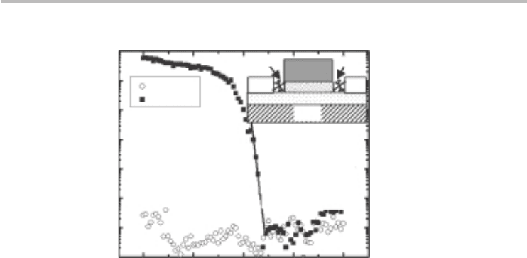
224 Chapter 8 Carbon nanotube field-effect transistors
–2
10
–13
10
–11
10
–9
Before
After
S = 69 m V/dec
10
–7
–1
0
1
2
V
g
(V)
I
d
(A)
S
OA
OA
D
CNT
LTO
SiO
2
Fig. 8.14 Room-temperature transfer characteristics of a top-gated CNFET showing unipolar
behavior after chemical doping of the nanotube contact extension regions (OA is the
charge transfer doping agent). The inset shows a cross-section of the device. Reprinted
with permission from J. Chen et al.
40
. Copyright (2005), American Institute of Physics.
technique to mitigate the OFF current is to engineer the gate flatband voltage such
that the transistor minimum current symmetry point is at V
G
= 0 V. However,
this technique is largely insufficient, since the minimum current at the symme-
try point has an exponential dependence on the drain voltage and is frequently
appreciable enough to prevent adequate ON/OFF current ratios.
39
Therefore, gen-
erally robust techniques are desirable for either suppressing ambipolar transport
or eliminating the OFF leakage current altogether. One promising technique to
obtain unipolar-like CNFETs is to engineer the nanotube device to be similar to a
conventional metal–oxide–semiconductor FET (MOSFET) with chemicallydoped
contacts while retaining an intrinsic channel. Figure 8.14 highlights the transfer
characteristics of an experimental CNFET with doped source/drain contact regions
showing unipolar behavior over a wide range of gate voltages and good switching
performance. In this device, the unipolar characteristic is attributed primarily to
the Schottky barrier reduction courtesy of the workfunction modification of the
source and drain electrodes under chemical doping.
40
At the moment, there are several challenges facing the routine fabrication of
chemically doped unipolar carbon transistors, including the synthesis of repeat-
able room-temperature air-stable p-type and n-type dopants for complementary
transistor applications. In addition, the doping concentration must be precisely
controlled and the dopants robust against any further device processing (such as
annealing or surface passivation), and must prove reliable over repeated transistor
40
J. Chen, C. Klinke, A. Afzali and Ph. Avouris, Self-aligned carbon nanotube transistors with
charge transfer doping. Appl. Phys. Lett., 86 (2005) 123108.

8.10 Paradigm difference between 2D FETs and 1D FETs 225
operation in the long term. Research in this direction is ongoing for CNFETs on
conventional and flexible substrates, and the desirable low-power advantages of
unipolar-like carbon transistors suggests that this pursuit will remain active for the
foreseeable future. In conclusion, it is gratifying that the intuition and understand-
ing gained from the device physics of ambipolar CNFETs extend to chemically
doped unipolar CNFETs with the pleasant benefit of simply neglecting ambipolar
(leakage) current. That is, electron current can be neglected in p-type devices and
vice versa.
8.10 Paradigm difference between conventional 2D MOSFETs and
ballistic 1D FETs
Charge transport in 1D ballistic FETs with transparent contacts represents a differ-
ent paradigm compared with conventional 2D MOSFETs. In this sense, ballistic
CNFETs with transparent contacts embody an ideal 1D FETwhere its narrow cylin-
drical nature confines mobile electrons to travel either forward or backwards in
one direction, while a conventional Si-MOSFETis an example model of a 2D FET,
where mobile electrons are free to move in a 2D plane. Furthermore, at comparable
length scales of practical relevance (∼10–100 nm), CNFETs afford ballistic trans-
port whereas diffusive transport dominates in a 2D MOSFET.
41
For these reasons,
charge transport in 1D FETs such as CNFETs reflects a different paradigm even
though the basic planar device geometry and current–voltage characteristics are
very similar. We must emphasize that other examples of ballistic 1D FETs that
experience this paradigm shift include ballistic nanowire and nanoribbon FETs of
sufficiently small width and ideal edge passivation.
Let us consider an ideal (textbook-like) long-channel MOSFET and a ballistic
CNFET to elucidate the similarities and differences in the main regimes of carrier
transport, including sub-threshold, linear, and active regions. In the sub-threshold
region, current in both devices is dominated by carriers above the gate-controlled
energy barrier, whose increase in the ideal case is fundamentally determined
by Fermi–Dirac thermodynamics. This is the origin of the room-temperature
60 mV/decade (i.e. 60 mV increase in V
G
leads to a decade increase in I
D
) sub-
threshold slope in transistors that operate by diffusion of over-the-barrier electrons.
In the linear region, charge transport in MOSFETs is by the process of drift, which
increases with the horizontal electric field (set by the drain voltage V
D
) and the
carrier mobility u
eff
. The carrier mobility is a useful parameter (related to the
mean free path) that in essence quantifies the average scattering of carriers in the
41
The longer mean free path of (low-energy) electrons in carbon nanotubes is arguably in part
because of its 1D nature, which leads to reduced DOS for backscattering, though we have yet to
see a rigorous exposition along this line.
226 Chapter 8 Carbon nanotube field-effect transistors
Table 8.3. Paradigm difference between conventional 2D FETs and ballistic 1D FETs
MOSFET (2D) CNFET (1D)
I
ON
≈ u
eff
C
ox
W
2L
(V
G
− V
T
)
2
I
ON
≈
k
B
T
eR
q
ln
1 + e
2eϕ
s
−E
g
2k
B
T
Parameter Origins Parameter Origins
(i) u
eff
drift velocity (i) ϕ
s
gate coupling
(ii) I/L drift velocity (ii) E
g
bandstructure
(iii) C
ox
/W charge sheet (iii) R
q
quantum transport
(iv) V
2
drift velocity (iv) k
B
T Fermi–Dirac
charge sheet thermodynamics
solid as they traverse the channel, and is a material-dependent property. For ballis-
tic CNFETs, current in the linear region is determined by the difference between
right-moving (from the source) and left-moving carriers (from the drain). In the
active region, MOSFET current saturates as a result of the pinch-off of the chan-
nel and, hence, the drift velocity is no longer dependent on the drain voltage.
For CNFETs, current saturation is due to carrier density invariance or saturation
because of the vanishing left-moving carriers from the drain. In other words, only
the right-moving carriers from the source exist in the channel; hence, the current
no longer depends on the drain voltage.
Based on the paradigm difference, it is possible to extrapolate and offer some
thoughts on comparative trends in channel length scaling by examining the ori-
gins of all the parameters in the ON state current expression for both devices as
enumerated in Table 8.3. We note that the ON current in Si-MOSFET is largely
controlled by the drift velocity, while that in a CNFET explicitly reveals many of
the fundamental physical properties of electrons in the solid-state material, such as
the bandgap, Fermi–Dirac thermodynamics, and quantum conductance. As such,
electrical properties as a function of scaling are invariably different. For exam-
ple, at high fields or for short channels, the drift velocity gradually saturates to
a constant, which leads to a different ON current expression for MOSFETs that
is not dependent on mobility or channel length and is quasi-linear with respect
to gate voltage. Overall, the Si-MOSFET does not scale gracefully to short chan-
nels.
42
In contrast, the ON current for CNFETs with transparent contacts reveals
no direct vulnerability to high-field effects. Indirect arguments can nonetheless
42
This is the reason why there have been many great engineering efforts to make up for the
degradation due to short-channel effects, including straining the channel to boost the current drive
and introducing high-mobility materials to serve as the channel, such as high-mobility III–V
semiconductors in place of the lower mobility silicon channel in an otherwise silicon-based VLSI
technology.

8.11 Summary 227
be made for some short-channel effects in CNFETs. A case in point is the conse-
quences of the increasing fraction of the channel length that is associated with the
length scale of optical phonon scattering (i.e. DOPS) at the drain contact, as was
highlighted previously. The short channel effects due to 2D electrostatic coupling
are, of course, common to both devices owing to their similar device geometry.
Additional non-idealities include gate leakage current due to thin oxides, possi-
ble band-to-band tunneling for low-bandgap materials, and direct source-to-drain
tunneling for ultra-short channel lengths. All in all, CNFETs have better immu-
nity to short channel effects and are expected to scale more gracefully to about
10 nm or so. Below 10 nm channel length, additional considerations, including
the impact of the precise scaling of λ, and quantum mechanical effects, such as
resonant tunneling phenomena, have to be examined carefully. Certainly, more
systematic experimental studies would obviously be most welcome in providing
a clearer picture of the scaling trend.
8.11 Summary
This chapter has provided an introduction to CNFETs with a primary emphasis on
the understanding of the basic electronic properties for the purpose of developing
intuition and insights. Some of the key device physics elucidated in this chapter
include:
(i) Ballistic transport in devices with transparent contacts offers the maximum
current.
(ii) Nanotubes operating inthe quantum capacitance limit have unique properties,
including voltage- and temperature-independent transconductance.
(iii) Ambipolar transport is characteristic of nanotube transistors that have direct
metal contacts (either Schottky barrier or ohmic).
(iv) Schottky barriers in general degrade the sub-threshold slope, reduce the con-
ductance, and limit the ON current. Sufficiently thin Schottky barriers have
properties close to CNFETs with transparent contacts.
(v) Unipolar-like nanotube transistors are achievable with doped contact regions.
(vi) There exists a paradigm difference between charge transport in conventional
MOSFETs and CNFETs.
Another insightful treatment of CNFETs (and nanoscale silicon FETs) can be
found in the work of Lundstrom and Guo.
43
Much of the device physics of CNFETs
readily extend to GNR transistors, and the analytical ballistic theory can be adapted
43
M. Lundstrom and J. Guo, Nanoscale Transistors: Device Physics, Modeling and Simulation
(Springer, 2006).

228 Chapter 8 Carbon nanotube field-effect transistors
to GNR transistors by taking into account their bandgap andthe number of degener-
ate subbands for low-energy transport. Ingeneral, the qualitative insights regarding
ballistic CNFETs also apply to diffusive-type CNFETs. However, an accurate
quantitative description has to properly take into account charge scattering and
non-equilibrium effects, such as carriers that may have gained sufficient energy
from the electric field or from absorbing aphonon and are no longer atthermal equi-
librium with the reservoir contacts. Such quantitative theories are often founded
on the quantum-mechanical non-equilibrium Green’s function (NEGF) formalism,
which is much more sophisticated but also computationally (time) expensive. The
interested reader will find the textbook by S. Datta a useful introduction to NEGF
formalism.
34
NEGF formalism is also very important in benchmarking the accu-
rary of analytical and compact nanotube transistor models, as we showed with
the analytical ballistic theory. An emerging nanotube transistor device that has not
been discussed is the tunnel CNFET that employs band-to-band tunneling as the
main voltage-controlled current mechanism.
44
This emerging device can offer a
steeper sub-threshold slope,resulting in lower power dissipation. Transistors based
on band-to-band tunneling are currently a matter of research.
Finally, it is highly desirable to have CNFETs with multiple nanotubes operating
in parallel so as to have control of the ON current and be able to supply arbi-
trary amounts, from micro-amperes to milli-amperes depending on the application
requirements.
26
For this reason, the study and application of CNFETs motivates
the ongoing research in growing aligned arrays of nanotubes. It is expected that
detailed analysis of the performance of CNFETs with multiple nanotubes will con-
tinue to inform the research on synthesis in order to achieve acceptable nanotube
densities (CNTs/micrometer) and narrow statistical distribution of diameters for
high-performance applications.
8.12 Problem set
All the problems are intended to exercise and refine analytical techniques while
providing important insights. If a particular problem is not clear, the reader is
encouraged to re-study the appropriate sections. Invariably, some problems will
involve making reasonable approximations or assumptions beyond what is already
stated in the specific question in order to obtain a final answer. The reader should
not consider this frustrating, because this is obviously how problems are solved in
the real world.
8.1. Quantum capacitance versus electrostatic capacitance in the sub-threshold
region.
44
J. Appenzeller, Y.-M. Lin, J. Knoch and Ph. Avouris, Band-to-band tunneling in carbon nanotube
field-effect transistors. Phys. Rev. Lett., 93 (2004) 196805.