Wong H.-S.P., Akinwande D. Carbon Nanotube and Graphene Device Physics
Подождите немного. Документ загружается.


8.3 Surface potential 199
where c
0
and c
1
are the Taylor series coefficients given by the lengthy expressions
c
0
=
C
ox
X [C
ox
(k
B
T )
2
Y
3
+ e
2
N
o
Z]
[C
ox
k
B
TX
2
+ e
2
N
o
e
(2m+1)E
g
/2k
B
T
]
2
(8.9)
where
X = e
E
g
/2k
B
T
+ Ae
E
g
/2k
B
T
Y = e
E
g
/2k
B
T
+ Ae
mE
g
/k
B
T
Z = Ae
E
g
(4m+1)/2k
B
T
(k
B
T − mE
g
) + e
E
g
(m+1)/k
B
T
(k
B
T + mE
g
)
c
1
=
e
2
C
ox
N
o
e
(2m+1)E
g
/2k
B
T
A
2
e
2mE
g
/k
B
T
− e
E
g
/k
B
T
#
C
ox
k
B
T
e
E
g
/2k
B
T
+ A e
mE
g
/k
B
T
2
+ e
2
N
o
e
(2m+1)E
g
/2k
B
T
$
2
. (8.10)
The useful property of these cumbersome expressions is that they explicitly
capture the dependence on C
ox
, bandgap, and temperature, albeit in a somewhat
complex manner. Ideally, if C
q
was linearly symmetric about eϕ
s
= 0.5E
cb
then a
natural choice for m corresponding to that point would be ∼0.25/e. However, C
q
is
generally not symmetric, as such, a value of m ∼(0.27/e) −(0.33/e) is found to give
the best agreement with numerical self-consistent computation. Finally, solving
for ϕ
s
in Eq. (8.8) yields the analytical surface potential in the semiclassical limit.
ϕ
s
≈
V
G
sV
G
+ t
, (8.11)
with s and t related to the Taylor series coefficients by
s =
c
1
c
0
, t =
1
c
0
. (8.12)
A similar analysis for holes (V
G
< 0) produces the same expression for the
surface potential with the exception that V
G
in the denominator of Eq. (8.11)is
replaced with |V
G
|. Employing Eq. (8.11), we arrive at a final algebraic relation
for the surface potential reflecting the influence of the gate in the quantum and
semiclassical limits:
ϕ
s
≈ V
G
− V
G
1 −
1
s|V
G
|+t
H
1 −
1
s|V
G
|+t
. (8.13)
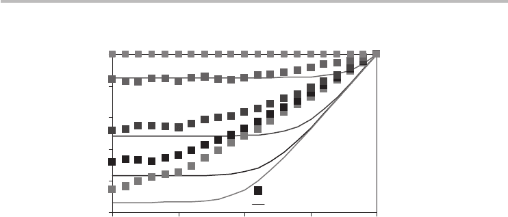
Figure 8.3 shows the surface potential computed numerically and analytically for
an example two-terminal top-gated CNT device. One terminal is the gate electrode
and the other terminal is the source and drain electrodes, which have been shorted
together (standard device connection for CNT capacitance measurements). The s
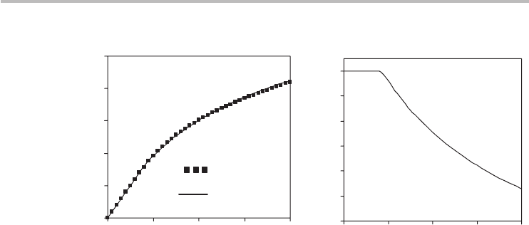
200 Chapter 8 Carbon nanotube field-effect transistors
0
0.1
0.2
0.3
0.4
0.5
0 0.2 0.4 0.6 0.8
00.20.40.60.8
w
s
for 1.5 nm CNT, and
HfO
2
oxide (k =15, t
ox
= 8 nm)
Self-consistent
computation
Analytical
calculation
0.4
0.5
0.6
0.7
0.8
0.9
1
V
G
(V)
w
s
(V)
w
s
/V
G
V
G
(V)
(a) (b)
Fig. 8.3 Characteristic profile of the CNT surface potential. Analytical ϕ
s
using best-fit parameters
(s = 1.41V
−1
, t = 0.76) compared with self-consistent computation showing good
agreement (peak error < 5 %). C
ox
∼ 264.96 aF µm
−1
. (b) Analytical ϕ
s
/V
G
revealing
that, at low voltages, V
G
has maximum control of the surface potential which gradually
weakens at higher voltages.
and t parameters used in Figure 8.3 (s = 1.41 V
−1
, t = 0.76) are the best-fit values
obtained empirically by curve fitting Eq. (8.13) to the numerical results. Using
m = 0.275/e and Eq. (8.12), the estimated analytical values for s and t are 1.52
V
−1
and 0.83 respectively, which are within 10 % of the best-fit values.
In summary, the Taylor series approximation has revealed that the appropriate
analytical form for the surface potential is Eq. (8.13) to first order, which shows
very strong agreement with numerically computed values of ϕ
s
. Additionally, the
analytical parameters (s and t) canbe determined from the Taylor series coefficients
with increasing accuracy as C
q
/C
ox
becomes smaller than unity.
8.4 Ballistic theory of ohmic-contact CNFETs
Employing the analytical surface potential discussed in the previous section, we
are now in a position to develop an analytical theory for CNFETs and thereby come
to an understanding of their basic transistor properties and performance metrics.
Of the four CNFETs identified in Table 8.1, the ballistic flavor with ohmic or
transparent contacts is the most attractive because it allows for the smoothest flow
of current, leading to superior performance compared with the other three flavors
of CNFETs. As a result, our focus here will be on the ballistic CNFET with ohmic
contacts. An added benefit is that the ballistic CNFET is actually the simplest
CNFET to study mathematically,
12
leading to deep insights that can be extended
12
While it is true that the ballistic CNFET is the easiest to study, it will not be fair if we failed to
mention that it is by far the most challenging of CNFETs to fabricate for reasons related to the
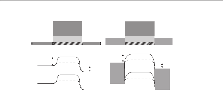
8.4 Ballistic theory of ohmic-contact CNFETs 201
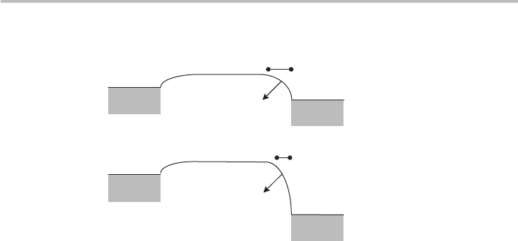
G
High-k
E
F
E
g
/2
eV
D
V
G
> 0
S D
V
G
= 0
S
D
G
High-k
SD
n++
intrinsic
E
cb
E
vt
E
g
/2
eV
D
V
G
= 0
V
G
> 0
(a) (b)
Fig. 8.4 Top-gated n-type CNFET device geometries considered within the ballistic model. (a) A
CNFET with doped CNT ohmic contacts and its band diagram. (b) A self-aligned CNFET
with ohmic metallic contacts and its band diagram (k = 15, t
ox
= 8 nm for the
experimental and analytical CNFETs analyzed in this section). Note that while electrons
experience an ohmic contact, holes, on the other hand, experience a Schottky barrier.
to the other types of CNFET in Table 8.1. Invariably, we expect a successful
transistor theory to capture all the pertinent parameters, including temperature and
bandgap. Additionally, the external voltages by which the charge and current are
controlled must be explicitly reflected in the transistor theory in order for the theory
to be of any use.
Ballistic transport in CNTs applies when the channel length is much smaller than
the electron mean free path l
m
. In high-quality semiconducting CNTs operating
around room temperature and at low energies, l
m
is essentially determined by
electron scattering from acoustic phonons which results in a mean free path of the
order of 0.5 µm.Therefore, high-quality CNFETs with channellengths 50 nmare
naturally suited for ballistic operation. Notably,the ballistic CNFET can be realized
in any of the device geometries shown in Figure 8.4. provided the channel length
and contacts satisfy the expected criteria. Figure 8.4 shows the simplified device
geometry of two top-gated CNFETs and associated band diagrams. In essence, the
gate voltage controls the energy barrier for current flow between the source and
drain electrodes, while the source and drain voltages control the source and drain
Fermi levels respectively.
The current–voltage (I −V ) relationship for a ballistic CNFET can be con-
structed from Planck’s quantum postulate. An alternative derivation based on the
DOS and group velocity can be found in previous studies.
13,14
We will focus on
difficulty of (i) making transparent contacts to semiconducting nanotubes and (ii) fabricating
small channel lengths.
13
K. Natori, Y. Kimura and T. Shimizu, Characteristics of a carbon nanotube field-effect transistor
analyzed as a ballistic nanowire field-effect transistor. J. Appl. Phys., 97 (2005) 034306.
14
D. Akinwande, J. Liang, S. Chang, Y. Nishi and H.-S. P. Wong, Analytical ballistic theory of
carbon nanotube transistors: experimental validation, device physics, parameter extraction, and
performance projections. J. Appl. Phys., 104 (2008) 124514.

202 Chapter 8 Carbon nanotube field-effect transistors
the n-type transistor (or n-CNFET for short) operation, where the contributions of
holes are considered negligible. The final results apply equally to p-CNFETs as
well. Planck’s quantum postulate relating the energy of the ith state to its frequency
can be explicitly rewritten in terms of the current from the particles occupying the
ith state:
E
i
= hf
i
=
h
2e
2e
τ
i
=
h
2e
I
i
, (8.14)
I
i
=
2e
h
E
i
, (8.15)
where f
i
and τ
i
are respectively the frequency and period of particles in the ith state.
For a system containing many states, the total current is the sum of the energy of
each state and the associated probability of occupation of the state:
I =
2e
h
i
F(E
i
, E
F
)E
i
, (8.16)
where F(E, E
F
) is the Fermi–Dirac statistic describing the probability that a state
with energy E is occupied by electrons and E
F
is the equilibrium Fermi energy:
F(E, E
F
) =
1
1 + e
E−E
F
k
B
T
. (8.17)
In the limit that the states are very dense (i.e. the spacing between the discrete
states becomes negligible), the sum can be converted to a Riemann integral:
I =
2e
h
F(E, E
F
) dE. (8.18)
In CNTs, there are right-moving carriers (electrons with positive velocities) and
left-moving carriers (electrons with negative velocities); hence, the net current
(commonly known as the drain current I
D
) is the difference between the right- and
left-moving carriers:
I
D
=
2e
h
dEF(E, E
F
) −
2e
h
dEF(E, E
F
− eV
D
). (8.19)
The Fermi energy of the right-moving carriers is controlled by the source potential,
while that of the left-moving carriers is controlled by the drain potential. We set
the source potential to 0 V for reference and, as such, for a positive drain voltage,
E
F
at the drain electrode will be correspondingly pulled down (see Figure 8.4b for
a visual illustration). Including the contributions of all the subbands in a semicon-
ducting nanotube, the total drain current becomes the sum of the net current from
8.4 Ballistic theory of ohmic-contact CNFETs 203
each subband:
I
D,tot
=
2e
h
j
∞
E
j
−eϕ
s
dE [F(E, E
F
) − F(E, E
F
− eV
D
)], (8.20)
where j is the subband index and E
j
is the energy minimum or bottom of the jth-
subband (for reference, E
j
for the first two subbands are shown in Figure 8.2). In
general, Eq. (8.20) is computed by numerical integration for the transistor drain
current. Fortunately, as a result of the analytical surface potential developed in
the previous section, we can obtain a simplified closed-form expression for the
drain current. The surface potential appropriate for a three-terminal device such
as a transistor will be elucidated towards the end of this section. At low operating
voltages characteristic of nanoscale technologies (supply voltages are typically
≤1 V), higher subbands can be ignored with negligible effect and Eq. (8.20),
therefore, simplifies to the contribution of the first subband.
15
I
D
=
4e
h
∞
E
cb
−eϕ
s
dE
[
F(E, E
F
) − F(E, E
F
− eV
D
)
]
. (8.21)
The additional factor of 2 in the prefix is due to the first subband degeneracy. It
follows that the integral yields an analytic formula for the drain current:
I
D
= I
o
%
ln
#
1 + e
2eϕ
s
−E
g
/2k
B
T
$
− ln
#
1 + e
2eϕ
s
−2eV
D
−E
g
/2k
B
T
$&
, (8.22)
where I
o
is
I
o
=
4e
h
k
B
T =
k
B
T
eR
q
, (8.23)
with R
q
representing the usual quantum resistance (R
q
= h/4e
2
∼ 6.45 k). At
300 K, I
o
∼ 4 µA. Equation (8.22) is the essential low-energy ballistic I−V for a
CNFET with transparent contacts as a function of the terminal voltages, material
properties, and temperature.
Let us take a moment to contemplate on the functional dependencies in the
formula and interpret its form. k
B
T comes about in the expression courtesy of
the thermodynamic Fermi–Dirac distribution, R
q
reflects the quantum transport of
carriers, and E
g
reflects the bandgap dependence. ϕ
s
captures the band structure of
the material (vis-à-vis the quantum capacitance) and also the effect of the external
15
Furthermore, Guo and coworkers have shown by computation (for an intrinsic ballistic CNFET)
that the first subband largely determines current under low-bias conditions. See J. Guo, A. Javey,
H. Dai and M. Lundstrom, Performance analysis and design optimization of near ballistic carbon
nanotube field-effect transistors. IEEE IEDM Tech. Digest, (2004) 703–6.

204 Chapter 8 Carbon nanotube field-effect transistors
gate voltage in controlling the channel charge. V
D
is the other external influence
by which charge transport can be controlled. The first term is the current from the
right-moving carriers, while the latter term is due to the left-moving carriers. An
important observation is that the current from the backward carriers is significant
in the linear region of the transistor I
D
−V
D
. The current from the forward carriers
determines the saturation current, also known as the ON current I
ON
, because at
high V
D
the latter term becomes negligible and the current saturates independent of
V
D
. We can obtain a rough estimate for the maximum I
ON
by reasonably assuming
that the maximum surface potential (in the low-energy ballistic regime) is slightly
greater than the energy minima of the first subband, say eϕ
s
∼ 1.5E
cb
= 0.75E
g
.
In this case, for d
t
from 1–3 nm at room temperature, the maximum first subband
I
ON
is within a factor of 2 of 24 µA. For a p-CNFET, Eq. (8.22) is modified by
reversing the polarity of ϕ
s
and V
D
.
I
D
= I
o
%
ln
#
1 + e
−(2eϕ
s
+E
g
)/2k
B
T
$
− ln
#
1 + e
(2eV
D
−2eϕ
s
−E
g
)/2k
B
T
$&
. (8.24)
The surface potential appropriate for a three-terminal device such as the CNFET
is slightly different from Eq. (8.1) defined in the previous section, which was
based on a two-terminal device structure where the source and drain are shorted
together. For the two-terminal device all the induced charges effectively travel
in the same direction, leading to a displacement current, and the purpose of the
surface potential is to account for all the induced charges in the nanotube. For the
case of a three-terminal device such as the n-type CNFET, at equilibrium, half
of the mobile electrons are right-moving carriers and the remaining half are left-
moving carriers. Hence, the appropriate surface potential to be used for a CNFET
(Eqs. (8.22)or(8.24)) must account for the charge carriers per direction in the
nanotube. That is, for example, the surface potential in the first or latter term of
Eq. (8.22) should account for only half of the induced charges, since those are the
charges moving with positive or negative velocities respectively. In this case, the
proper definition for the surface potential for CNFETs is
ϕ
s
=
C
ox
C
ox
+
C
q
(ϕ
s
)
2
V
G
=
2C
ox
2C
ox
+ C
q
(ϕ
s
)
V
G
(8.25)
where the factor of 2 represents the fact that only half the charges are traveling in
any particular direction at any gate voltage with V
D
= 0. This is, of course, similar
to Eq. (8.1); as such, the analytical expression developed for the surface potential
(Eq. (8.13)) can still be employed with C
ox
replaced with 2C
ox
in the expressions
for the model parameters, s and t. Under excitation, the role of a finite V
D
is to
suppress the backward carriers in a CNFET.
An additional concern that needs to be incorporated in a general formulation
for the surface potential is the flatband voltage V
FB
.
16
All along we have been
16
In a nutshell, the flatband voltage is the voltage applied to the gate to get a flat energy band
diagram along the vertical cross-section of the device, and is given by V
FB
=
MS
where
MS
is
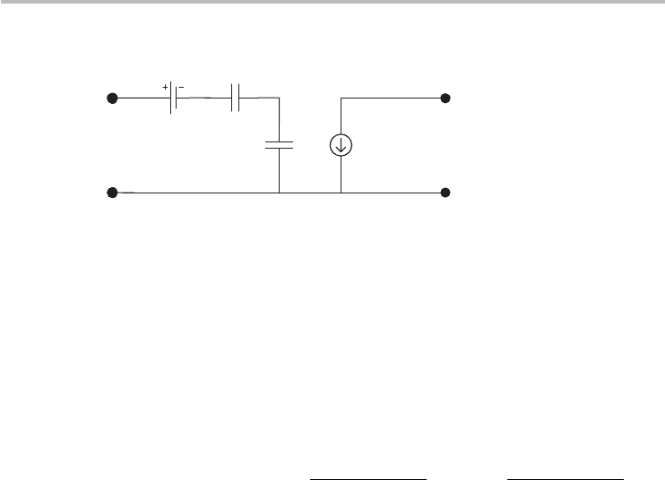
8.4 Ballistic theory of ohmic-contact CNFETs 205
ϕ
s
C
q
/2
C
ox
V
FB
I
D
=f (ϕ
s,
V
DS
)
G
S
D
+
–
Fig. 8.5 An electrostatic intrinsic circuit model of the ballistic CNFET.
using V
G
assuming flatband conditions at V
G
= 0 V. In general, inclusion of the
workfunction difference between the gate metal and the nanotube leads to
V
G
= V
G
+ V
FB
, (8.26)
where V
G
is the voltage under flatband conditions. The expression for V
G
should
be used in the formula for the surface potential:
ϕ
s
=
(
V
G
− V
FB
)
1 −
1 −
1
s|V
G
− V
FB
|+t
H
1 −
1
s|V
G
− V
FB
|+t
.
(8.27)
For a non-zero voltage at the source electrode, V
GS
and V
DS
should be used instead
of V
G
and V
D
respectively in the expressions for the drain current and surface
potential. An intrinsic electrostatic (sometimes called large-signal) circuit model
of the ballistic CNFET is shown in Figure 8.5.
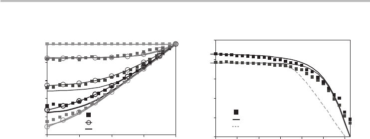
The value of analytical theories depends on how successfully the theory corrob-
orates experimental observations. For this purpose, the analytical ballistic theory,
Eq. (8.24), is compared in Figure 8.6 with an experimental ballistic p-CNFET
reported by Javey et al.
17
The model parameters used are identical to the values
reported for the experimental CNFET (d
t
= 1.7 nm, E
g
= 0.5 eV, and device
geometry shown in Figure 8.4b), including a parasitic source/drain metal resis-
tance of 2 k each, which is close to the reported estimate of ∼1.7 k. Parameter
extraction of the flatband voltage from the experimental data yielded a value of
V
FB
∼ 0.28Vwhich is used in the comparison.
14
Amodest agreement is observable
in the active or current saturation region, while in the linear region the analytical
ballistic theory significantly overestimates the current and conductance. The origin
of the discrepancy can be identified upon closer examination of the band diagrams
in Figure 8.4, and is elaborated upon in the next section.
the workfunction difference between the gate and the semiconductor. Basically, for a positive or
negative V
FB
the action of the gate is retarded or enhanced respectively in an n-CNFET, and vice
versa for a p-CNFET. Enhancement (retardation) implies less (more) voltage is needed to turn ON
the device.
17
A. Javey, J. Guo, D. B. Farmer, Q. Wang, E. Yenilmez, R. G. Gordon, et al., Self-aligned ballistic
molecular transistors and electrically parallel nanotube arrays. Nano Lett., 4 (2004) 1319–22.
206 Chapter 8 Carbon nanotube field-effect transistors
–25
–20
–15
–10
–5
0
–0.4 –0.3 –0.2 –0.1 0
V
DS
(V)
V
G
from 0.2 to –1 V
–0.3 V steps
Experimental (A. Javey)
Analytical ballistic theory
l
D
(µA)
Fig. 8.6
Experimental results and analytical model predictions, Eq. (8.24), for a ballistic 50 nm
p-type CNFET (identical to Figure 8.4b). s = 1.6 and t = 0.82 for the analytical φ
s
.
Agreement is good in the active region but weak in the linear region due to optical phonon
scattering, which needs to be accounted for in the theory. (Experimental results are
courtesy of Javey et al.
17
)
8.5 Ballistic theory of CNFETs including drain optical
phonon scattering
So far we have found the ballistic theory of CNFETs to be in modest agreement
with experimental data in the current saturation or active region of the I −V curve.
However, a significant discrepancy exists in the linear region. A closer scrutiny of
the band diagram of the ballistic CNFET proves useful in providing guidance as to
the way forward to an improved theory. Figure 8.7 illustrates the conduction band
diagram of an n-CNFET under two drain bias conditions. Figure 8.7aisatalow
drain bias corresponding to the linear region, while Figure 8.7b corresponds to the
saturation region. Wecan see visually that otherwise low-energyelectrons traveling
through the channel towards the drain will acquire significant energy at the drain
end of the channel.
18
This forces us to re-examine our assumption of ballisticity.
While it is true that electron transport through most of the channel is ballistic (a flat
band signifies a ballistic channel without resistive voltage drop), at the drain end
the prospect of optical phonon scattering characteristic of high-energy particles is
certainly possible. In CNTs, the criteria to be satisfied for electron scattering by
optical phonons is that (i) the length of travel through the well l
w
, (see Figure 8.7)
should be greater than the optical phonon mean free path (l
op
∼ 10 nm) and (ii) the
energy of the electrons must be greater than the critical optical phonon emission
18
The kinetic energy of the electrons is the excess energy acquired beyond the conduction band
energy minima.
8.5 Ballistic theory of CNFETs 207
V
D
< V
T
V
D
< V
T
l
w
> l
op
l
w
> l
op
S
S
D
D
Significant optical
phonon scattering
Negligible optical
phonon scattering
(a)
(b)
Fig. 8.7
Illustration of optical phonon scattering in a ballistic (n-type) CNFET. (a) At low V
D
, the
length of the triangle-like well l
w
is comparable to the mean free path of optical phonon
scattering (l
op
∼ 10 nm), thereby reducing I
D
. (b) At higher V
D
, the well is sharpened,
becoming gradually less than l
op
and, hence, having a minimal effect on I
D
. This device
physics can be captured to first-order by the DOPS parameter α, which accounts for the
reduced current.
energy (E
op
∼ 0.16 eV; see Chapter 7). If these conditions are satisfied,
19
then
optical phonon scattering will occur at the drain end of the channel and, hence, the
current (and conductance) in the linear region will be reduced accordingly, cor-
roborating experimental observations. At higher drain bias (saturation region), the
triangular well becomes steeper,
20
with an ever-decreasing length, which implies
that electron scattering by optical phonons becomes negligible as l
w
< l
op
, leading
to minimal correction of the ballistic theory in the active region.
The scattering of high-energy electrons by optical phonons in an otherwise
ballistic channel can be incorporated into the ballistic theory by a phenomenolog-
ical parameter which is rightly called the drain optical phonon scattering (DOPS)
parameter α. The justification of this parameter is as follows. Optical phonon
scattering at the drain end essentially implies a localized resistance leading to an
effective drain voltage across the ballistic portion of the channel that is less than
the terminal drain voltage. In this light, we can construct a DOPS parameter to
quantify the effective or reduced drain voltage. It follows that the effective drain
voltage can be written phenomenologically as αV
D
where 0 <α≤ 1, leading to
a more realistic expression for the drain current:
I
D
= I
o
%
ln
#
1 + e
(±2eϕ
s
−E
g
)/2k
B
T
$
− ln
#
1 + e
(±2eϕ
s
∓2eαV
D
−E
g
)/2k
B
T
$&
,
(8.28)
19
It can be shown that the conditions can be satisfied in the linear region of the I −V by employing
semiconductor junction theory.
20
In semiconductor device physics, the potential well is often considered a carrier depletion region
and modeled as a capacitance. At higher drain voltages, the electrostatic attraction is greater,
thereby pulling the electrons closer to the drain side, resulting in a steeper potential well.
208 Chapter 8 Carbon nanotube field-effect transistors
–25.00
–20.00
–15.00
–10.00
–5.00
0.00
–0.4 –0.3 –0.2 –0.1 0
V
DS
(V) V
GS
(V)
V
G
from 0.2 to –1 V
–0.3 V steps
Experimental (A. Javey)
Computation (J. Guo)
Analytical ballistic theory
I
D
(µA)
–1 –0.8 –0.6 –0.4 –0.2 0 0.2
10
–4
10
–5
10
–6
10
–7
10
–8
10
–9
–I
D
(A)
Experimental (A. Javey)
Analytical ballistic theory
Analytical (C
q
=C
q
,
metallic
)
V
D
= –0.3 V
V
D
= –0.1V
(a) (b)
Fig. 8.8 (a) I
D
−V
DS
including the DOPS parameter (α = 0.5) showing strong agreement between
analytical ballistic theory Eq. (8.28), experimental results, and quantum mechanical
computation. (b) Likewise, I
D
− V
GS
also results in strong agreement with experimental
data in active, linear, and sub-threshold regions. The dashed line (V
D
=−0.1 V) is the
analytical prediction if C
q
= C
q,metallic
is assumed, as is sometimes employed in compact
modeling of semiconducting CNTs, leading to gross errors in the sub-threshold and active
regions but which is fairly accurate in the linear region. (Experimental and quantum
mechanicalcomputationdataarecourtesyofA.Javey,J.Guo,etal.
17
)
where the upper polarity is for n-CNFETs and the lower polarity is for p-CNFETs.
In general, α should depend on both the gate and drain voltages, since they con-
trol the length and energy of the triangular well. For the greatest simplicity, let us
consider the DOPS parameter a constant which is extractable from experimental
data.
21
Returning to the experimental data of Javey et al.,
17
the maximum channel
conductance value of ∼0.5/R
q
was reported corresponding to α ∼ 0.5. Employing
this value of α, we observe that the DOPS-corrected ballistic current, Eq. (8.28),
is justified by the remarkably strong agreement with the experimental data in all
major regions of transistor operation (sub-threshold, linear, and saturation), as
shown in Figure 8.8. Detailed self-consistent quantum mechanical computations
reportedbyJ.Guofortheexperimentaldevicearealsoincludedforreference,
17
demonstrating the strength of the analytical ballistic theory in accurately repro-
ducing the experimental and quantum mechanical results. The slight disagreement
in the OFF state (V
G
∼ 0.2 V in Figure 8.8b) is due to ambipolar electron current,
which can be handled within the Schottky-barrier CNFET model developed in
Section 8.8.
In order to provide clarity in the use of the term ballistic transport in transistors,
it is necessary to make two distinctions:
(i) Fully ballistic transport:This isdefined as transport with no acoustic or optical
phonon scattering (α = 1).
21
The DOPS parameter α can be extracted from measurements of the drain to source channel
conductance (g
ds
), in the limit of V
D
→ 0, and V
G
→ V
DD
where V
DD
is the drain supply
voltage. In this limit, the conductance is g
ds
= α/R
q
.