Venables J. Introduction to Surface and Thin Film Processes
Подождите немного. Документ загружается.

needed. Monte Carlo modeling of electron scattering in solids has been developed to
study contrast mechanisms, including high spatial resolution studies of analytical tech-
niques based on SEM and SAM (El Gomati et al. 1979, Shimizu & Ding 1992).
Following on the discussion in section 3.4, we can think about the extraction of
Auger data from energy-selected line scans and images, and the quantification of such
information. We need to use ratio techniques for several reasons. First, typical samples
are not flat, and may be extremely rough, or can involve changes in backscattering
factor. This leads to variations in (rsec
u
0
·T); such changes in the Auger peak channel
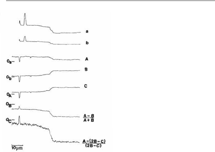
(A) can often go in the opposite direction from what is expected, for example in figure
3.22. In this case, the back-scattering from the Ag islands is less than that from the W
substrate. Thus the signal at channel A reduces as the scan crosses the islands; but at
the background channel B, it reduces more.
Second, one needs to have Auger information which (if possible) is independent of
these changes in the background spectrum, and of beam current fluctuations. The first
goal is not entirely possible, but one can make a good attempt. By taking line scans or
images at one or more energies in the background above the peak (B and maybe C),
then difference techniques can be constructed to extract better Auger information. The
ratio most commonly used is a quasi-logarithmic measure of Auger intensity based on
two channels only,
I(difference)/I(sum)5(A2 B)/(A1B), (3.17)
3.5 Microscopy-spectroscopy 97
Figure 3.22. Biased secondary and Auger line scans of the edge shown in figure 3.21.
Secondary electron scans (a) and (b) with and without zero suppression respectively. Energy
selected line scans at A 346, B 385 and C 424 eV electron energy images, plus Auger line scans
based on the algorithms shown (after Jones & Venables 1985, reproduced with permission).

which is a first approximation to (2EN(E))
21
·d(EN(E))/dE ) in the fixed retard ratio
mode (Janssen et al. 1977, Prutton et al. 1983). The simplest linear measure is based on
an extrapolation of the background from C to B to A. Assuming these channels are
equally spaced, then the
Peak to background ratio (P/B)5 (A22B1C)/(2B2C). (3.18)
We can see from figure 3.22 that this measure is usually noisier than the ratio based on
the two channels A and B, as discussed in some detail by Frank (1991). This is because
one is in effect measuring the background slope at each pixel, as well as the peak height.
If you are unhappy about the noise level in images, you can always trade SNR for image
resolution by digital image processing. The result is not always very pleasing, nor even
necessary, since the eye does this for you anyway. It is amazing how well our eyes/brain
are able to extract feature information from very noisy data. These issues, which are
common to many imaging and analysis techniques, can be explored further via
problem 3.3.
3.5.2 Auger and image analysis of ‘real world’ samples
A particular problem faced by analysts in the ‘real world’ is that their samples contain
many different elements; they may have rough surfaces, and this may interfere with
quantitative analysis. However, they may not be so concerned about quantitative infor-
mation at every point in the image; association of specific types of qualitative informa-
tion with each point may be more informative. This type of ratio technique has been
developed by several groups, and an illustration is given in figure 3.23 (Browning 1984,
1985). Prutton’s group at York has furthered these techniques, originally developed for
satellite imaging by NASA/JPL, as described in more recent papers (Walker et al. 1988,
Prutton et al. 1995).
In such an approach an SEM picture is taken of the whole field of view and a survey
spectrum is taken from this area. This shows many peaks, some of them very small
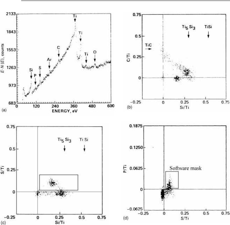
(figure 3.23(a)). The spectrum is used to identify energies (channels) at which informa-
tion will be recorded at each point on the image, typically a peak and a background
channel at higher energy, for each of the elements of interest. This information is col-
lected and stored digitally. Before images are made with this information, scatter dia-
grams, such as figures 3.23(b), (c) and (d) are constructed. These show that the ratio
data cluster in well defined regions of the scatter diagram, and it is easy for the analyst
to identify the clusters as particular phases, at least tentatively.
At this stage, one can put a software ‘mask’ over the data, as shown schematically
by the rectangles in figure 3.23(c) and (d), and use all the data which fall within this
mask to form an image. An unknown phase was identified which contained Ti, Si,
some S and also P. By setting limits on the various ratios, an image can now be pro-
duced from the stored data set, which shows the spatial distribution of this particular
range of compositions. In this case it was shown that the ‘phase’ was formed in the
reaction zone between the SiC fiber and the Ti alloy which made up the composite
material.
A simpler two component system, such as an evaporated tungsten pad on silicon can
98 3 Electron-based techniques
be used to explain the principles clearly (Kenny et al. 1994). There is no real limitation
to 2D data; experiments with 3D data sets have been reported in this same paper. These
‘associative’ or pattern recognition techniques are very powerful, but they do require that
a lot of effort be expended on a particular small area. This concentration on one small
area may well result in radiation or other forms of damage, and it is always possible that
you could have got the answer you really needed faster by another technique. At high
spatial resolution one needs to beware of various artifacts associated with sharp edges,
essentially because part of the information comes from backscattered electrons. Some of
these effects were studied by El-Gomati et al. (1988), and are discussed by Smith (1994),
Kenny et al. (1994) and Prutton et al. (1995).
3.5 Microscopy-spectroscopy 99
Figure 3.23. Use of scatter diagrams and ratio techniques for an early example of image
analysis, adapted from Browning (1984) and reproduced with permission: (a) a survey E·N(E)
spectrum from an anomalous region in the reaction zone between a Si fiber and the
Ti–6A1–4V alloy matrix; (b)–(d) ratioed scatter diagrams for (b) C/Ti, Si/Ti, (c) S/Ti, Si/Ti and
(d) P/Ti, S/Ti. A software mask is indicated on (d), setting limits on the ratios P/Ti and S/Ti,
with a less restrictive mask for Si/Ti on (c). See text for discussion.
3.5.3 Towards the highest spatial resolution: (a) SEM/STEM
The development of SEM/STEM and AES/SAM at the highest resolution has been
pursued at Arizona State University in what has become known as the MIDAS project,
a Microscope for Imaging, Diffraction and Analysis of Surfaces. Figures 3.24–3.27 are
shown here to illustrate this project, which is described in more detail by Hembree &
Venables (1992).
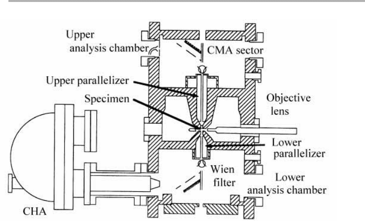
The innovation as regards electron optics is to use the spiraling of the low energy
electrons in the high magnetic field of the objective lens to contain the secondary and
Auger electrons close to the microscope axis. These electrons are further controlled by
auxiliary magnetic fields (parallelizers on figure 3.24) in the bores of the lens, and by
biasing the sample negatively. A special combination Wien filter/deflector is then used
to deflect the low energy electrons off axis through a right angle, while keeping the 100
keV beam electrons on axis. The low energy electrons then enter a commercial CHA.
Because they spiral in the high B field and their angle to the axis decreases as the field
weakens, quite a large proportion of the emitted electrons can be collected. This higher
collection angle compensates for the lower yield at higher beam energy, and the smaller
current available in the fine probe.
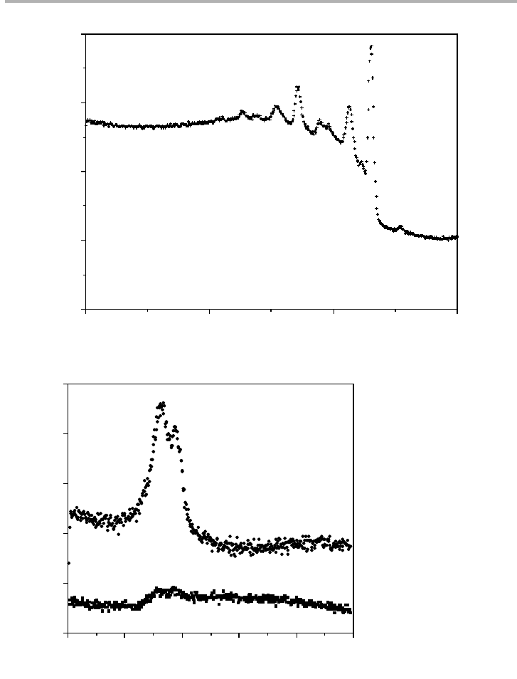
The quality of the spectra obtained is relatively high, both with respect to energy res-
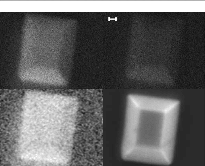
olution (figure 3.25(a)) and to sensitivity (figure 3.25(b)). Auger mapping is obtained by
taking images A and B and using ratios (A2 B)/(A1B) as explained above. Figure 3.26
shows the comparison of the b-SE image, with good SNR, and the Auger image, with
relatively poor SNR, even after smoothing. For imaging, we have to be clear about dis-
tinctions between ‘image’ and ‘analytical’ resolution. This is because of the non-local
100 3 Electron-based techniques
Figure 3.24. Cross sectional diagram of the specimen region of the MIDAS column, showing
the relationship of parallelizer coils, objective lens, extraction optics and the sample (after
Hembree & Venables 1992, reproduced with permission).
3.5 Microscopy-spectroscopy 101
Figure 3.25. Pulse counted Auger electron spectra obtained with the 100 keV probe in MIDAS
(a) Si KLL from clean Si (10 nA probe current, 10 min acquisition time for 512 point
spectrum); (b) Ag MNN from 100 nm wide island on Si(001) and from ,0.5 ML Ag layer
between the islands (1.6 nA probe current, in 10 min (upper data) and 20 min (lower data) for
the two cases respectively) (after Hembree & Venables 1992, reproduced with permission).
420400380360340320
500
1000
1500
2000
2500
3000
Electron Energy (eV)
Intensity (cps)
(b)
1700160015001400
20000
40000
60000
80000
100000
Electron Energy (eV)
Intensity (cps)
(a)
nature of the Auger signal, firstly from backscattered electrons as discussed already, but
also at high spatial resolution because of the finite Auger attenuation length, and non-
local excitation. Image resolutions below 3nm have been obtained on bulk samples in
this instrument.
In the case of thin film substrates, we largely eliminate the backscattering contribu-
tion, so that the image and analytical resolutions converge on the image resolution,
which in practice may well be limited by the probe size. Such high resolutions are of
interest in small particle research, particularly in catalysis. The old joke used to be that
if you can see the particle in an electron microscope, then it was already too large to be
a useful catalyst. Analysis of such a particle is even harder, especially if one is inter-
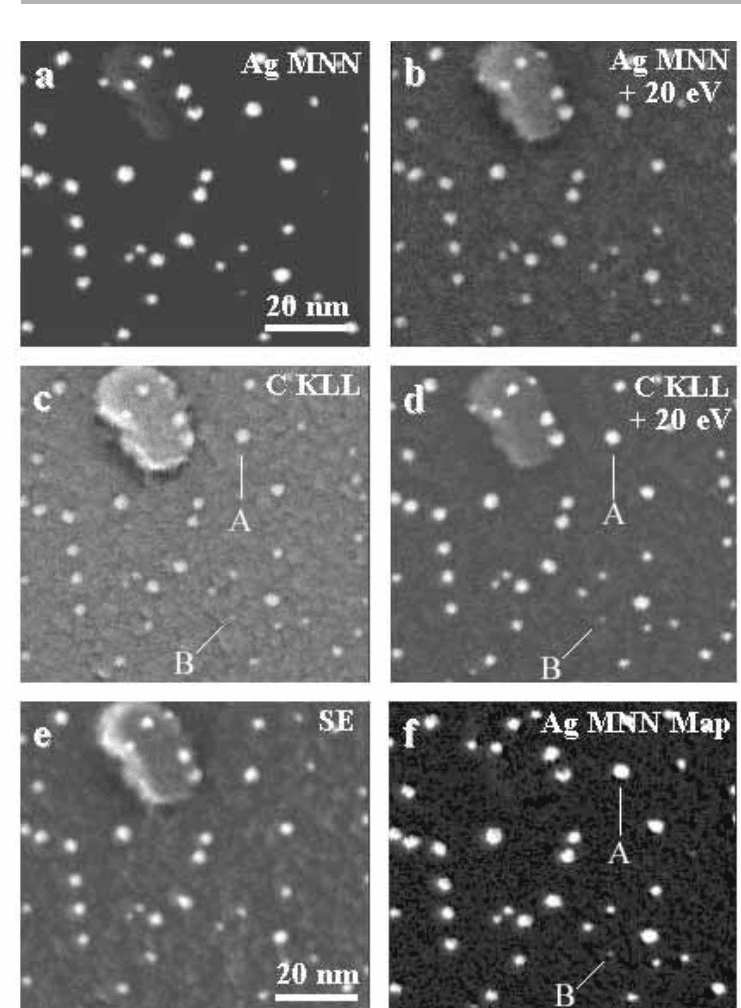
ested in minority elements. Work on such samples has been pursued by Liu et al. (1993)
as illustrated in figure 3.27, which shows energy selected images of small Ag particles
on a thin carbon substrate.
Here it is not so clear what the quantification routine ought to be, and in practice
Auger information has been portrayed using the raw A and B and simple difference
(A2 B) images for various elements. Even for small Ag particles, backscattering effects
can be seen in the intensity of carbon Auger peak images (figure 3.27(c) and (d)), but
102 3 Electron-based techniques
Figure 3.26. Energy selected electron images, Ag MNN Auger intensity map derived from
those images and biased secondary electron image of three-dimensional silver island on Si
(001), with probe current 1.5 nA, 20 min acquisition time for energy selected images; 0.3 nA
and 1 min for b-SEI (after Hembree & Venables 1992, reproduced with permission).
20 nm
Ag Peak
Ag MNN
b-SEI
Background
3.5 Microscopy-spectroscopy 103
Figure 3.27. Energy selected electron images of the same area containing small Ag particles on
a thin amorphous carbon substrate obtained using different signals in MIDAS: (a) Ag MNN;
(b) Ag MNN120 eV; (c) C KLL; (d) C KLL120 eV, (e) low energy SE, and (f) P
Ag
2 B
Ag
(after Liu et al. 1993, reproduced with permission). The larger (A) and smaller (B) particles
indicated in panels (c), (d) and(f) lie just off the upper end of the corresponding drawn lines.
See text for discussion.
()
)
)
)
)
)
(
(
(
(
(

the carbon background is largely removed in the Ag difference image (figure 3.27(f)).
Secondary electrons (figure 3.27(e)) show a very similar information to energy selected
images, via the higher secondary yield of Ag. Even more interesting is that, for parti-
cles of size at or below the Auger attenuation length, the number of atoms in the cluster
is measured by the integrated intensity of the particle, rather than the image size of the
particle, and that such images can be internally calibrated, using large particles such as
A in figure 3.27(f). On this basis, it was concluded that particles such as B in this panel
(clearly visible in the original, as all microscopists say) contained ,10 Ag atoms.
We should note that, because of the high yield for Ag MNN Auger electrons, this is
a favorable case; we are still quite a way from detecting arbitrary minority species on
such small particles. Moreover, we are much more likely to be able to detect them first
with a high SNR, qualitative, technique, such as b-SEI, than with low SNR, quantita-
tive AES/SAM. There are more recent illustrations of this point coming from MIDAS.
For example, oxygen KLL at 505 eV has a relatively low Auger yield. Small oxide par-
ticles on copper can be seen very readily in high resolution b-SE images. Indeed the
presence of oxide can be seen in the shape of the (secondary electron) spectrum back-
ground, whereas wide beam Auger declares the surface to be clean (Heim et al. 1993).
This discrepancy is due both to the fact that the oxide particles cover a small fraction
of the surface, and that oxides in general have a very high secondary electron yield.
3.5.4 Towards the highest spatial resolution: (b) scanned probe
microscopy-spectroscopy
Following the revolutionary development of STM by Binnig, Rohrer and co-workers
in 1982–83, it is now almost routine that atomic resolution can be obtained on a wide
variety of samples, and, in contrast to the example described in the last section, many
groups have achieved such resolution, even under UHV conditions. Indeed, these tech-
niques are now so widespread that recent reviews of UHV-based STM have been spe-
cialized to particular materials, e.g. metals (Besenbacher 1996) or semiconductors
(Kubby & Boland 1996, Neddermeyer 1996).
In my lecture courses, the use of spectroscopy in STM (or other scanned probe)
instruments has typically been discussed in a student talk. In principle, such spectro-
scopic information allows one to identify surface atomic species in favorable cases, if
not in general. This is because the STM/STS techniques (Feenstra 1994) probe the
valence and conduction bands, which may be sensitive to atomic species, but are not
chemical specific in the same sense as AES/SAM. This is not unlike the SEM/SAM dis-
tinction; STM/STS may well be able to perform ‘chemical’ identification possible out
of a range of possibilities, due to a combination of atomic resolution and changes of
contrast due to electronic effects, and in particular due to a high SNR.
One of the many amazing positive features of STM/STS is that the probing current
is also the signal, which may be between 1nA and 1pA. In AES/SAM used on a micro-
scopic scale, the probing current may be between 100 nA and 10pA, but the collected
current is down to maybe 100000 times smaller than the probe current, which does not
do good things for the SNR. Thus one typically has to think very carefully about what
104 3 Electron-based techniques

information is wanted and is practicable to obtain. Some of the examples given in this
section are close to the current technical limits. Rather than laboring the virtues of
STM, STS, AFM, etc., in this and other respects, specific results are used to illustrate
points being made as they arise in the text. To get started in this area, one can consult
the references given in section 3.1.3 and the web-based resources listed in Appendix D.
Further reading for chapter 3
Briggs, D. & M.P. Seah (1990) Practical Surface Analysis, vols. I and II (John Wiley).
Buseck, P., J.M. Cowley & L. Eyring (Eds.) (1988) High Resolution Transmission
Electron Microscopy and Associated Techniques (Oxford University Press) especially
chapter 13: Surfaces by K. Yagi.
Chen, C.J. (1993) Introduction to Scanning Tunneling Microscopy (Oxford University
Press), especially chapter 1 and the photographic plates which precede this chapter.
Clarke, L.J. (1985) Surface Crystallography: an Introduction to Low Energy Electron
Diffraction (John Wiley).
Feldman, L.C. & J.W. Mayer (1986) Fundamentals of Surface and Thin Film Analysis
(North-Holland).
Lüth, H. (1993/5) Surfaces and Interfaces of Solid Materials (2nd/3rd Edns, Springer),
panels 2, 3 9 and 11, and chapter 6.
Moore, J.H., C.C. Davis & M.A. Coplan (1989) Building Scientific Apparatus (2nd Edn,
Addison-Wesley) chapter 5.
Prutton, M. (1994) Introduction to Surface Physics (Oxford University Press), chapters
2 and 3.
Rivière, J.C. (1990) Surface Analytical Techniques (Oxford University Press).
Stroscio, J. & E. Kaiser (Eds.) (1993) Scanning Tunneling Microscopy (Methods of
Experimental Physics, Academic), volume 27.
Smith, G.C. (1994) Surface Analysis by Electron Spectroscopy (Plenum).
Walls, J.M. (Ed.) (1990) Methods of Surface Analysis (Cambridge University Press).
Wiesendanger, R. (1994) Scanning Probe Microscopy and Spectroscopy (Cambridge
University Press) especially chapters 4 and 5.
Woodruff, D.P. & T.A. Delchar (1986, 1994) Modern Techniques of Surface Science
(Cambridge University Press) especially chapters 2 and 3.
Problems, talks and projects for chapter 3
These problems, talks and projects are to test and explore ideas about surface tech-
niques and surface electronics.
Problem 3.1. Some questions on surface techniques
Give a short description of the following points in relation to surface techniques,
including some examples.
Problems, talks and projects for chapter 3 105

(a) Explain why we say that we have conservation of k
//
, but not of k
⬜
, in surface scat-
tering experiments.
(b) Explain why surface X-ray diffraction can be understood quantitatively in terms
of ‘kinematic’ scattering, whereas the various forms of electron diffraction require
a ‘dynamic’ theory.
(c) Explain why the lineshape in UPS is said to reflect the ‘valence band density of
states’ whereas the AES lineshape may depend on a ‘self-convolution of the VB
DOS’.
(d) Explain the experimental setup, and energy resolution, needed to observe surface
phonons. Comment on the relative energy resolution required for inelastic photon
(Raman), electron (HREELS) and helium atom scattering.
Problem 3.2. The role of inelastic scattering in LEED
A quasi-kinematic model of LEED is possible based on the following assumptions.
The inner potential of the crystal, is V
0
⬃ 10V, which increases the wavevector in the
crystal over that in free space and refracts the beam at the surface. The attenuation of
the incident beam amplitude (and the back-diffracted beams) is exponential with a
short mean free path
l
, which is inversely proportional to the imaginary potential V
0i
⬃ 3–5V. A single backscattering event happens at a given atom at depth z, and has scat-
tering factor f (or equivalently t, the t-matrix) which is a function of the beam energy
E and the scattering angle
u
.
Assuming that the surface plane is (001), do the following.
(a) Draw the LEED geometry and Ewald sphere, with a plane wave input beam not
necessarily perpendicular to the surface.
(b) Write down an expression for the scattered amplitude from a crystal into the (hk)
reciprocal lattice rod, where the spacings between layers parallel to the surface are
not necessarily equal to the bulk spacing.
(c) Work out the scattered intensity distribution I(V) along the (hk) rod for the case of
normal incidence, where the spacings are equal to the bulk spacing, and draw the
intensity profile.
(d) Show that the peak positions and spacings can be used to calculate the c-plane
spacing, and V
0
if f is real. Show that the width of the peaks is inversely related to
l
, and hence directly to V
0i
.
Problem 3.3. The importance of a high SNR in AES
One of the main problems in Auger electron spectroscopy is that the signal rides on
a non-negligible background, and that the signal to noise ratio (SNR) and the
peak/background ratio (P/B or PBR) can be small. This leads to long data collection
times and/or noisy signals, which are especially troublesome for imaging. The schemes
discussed in section 3.5 are attempts to approximate the desired ratio signal with a
simple algorithm which can be implemented using digital data collection and process-
106 3 Electron-based techniques
