Справочник по мощным TMOS транзисторам (MOTOROLA)
Подождите немного. Документ загружается.

4–8
Motorola TMOS Power MOSFET Transistor Device Data
, DISCHARGE CURRENT (mA)I
dscg
–60
12.5
0
14.0
0
2.5
10
16
0
1.0
0
–200
V
th(UVLO)
, UNDERVOLTAGE
T
A
, AMBIENT TEMPERATURE (°C)
Startup Threshold
V
CC
Increasing
I
Source
, OUTPUT SOURCE CURRENT (mA)
V
CC
= 15 V
V
Pin
4
= 0 V
V
Pin
1
= 1.0 V
Pin 8 = Open
T
A
= 25°C
V
Pin
8
, INPUT VOLTAGE (V)
V
O
, D
RI
V
E
O
UT
P
UT
VO
LT
AG
E
(
V
)
V
CC
, SUPPLY VOLTAGE (V)
V
Pin
4
= 0 V
T
A
= 25°C
V
Pin 7
, FA
ULT
O
UT
P
UT
VO
LT
AG
E
(
V
)
I
Sink
, OUTPUT SINK CURRENT (mA)
V
CC
= 15 V
V
Pin
4
= 5.0 V
T
A
= 25°C
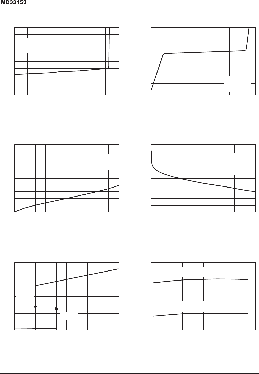
Figure 21. Fault Blanking/Desaturation
Current Source versus Input Voltage
V
Pin
8
, INPUT VOLTAGE (V)
Figure 22. Fault Blanking/Desaturation Discharge
Current versus Input Voltage
V
CC
= 15 V
V
Pin
4
= 0 V
T
A
= 25°C
Figure 23. Fault Output Low State Voltage
versus Sink Current
Figure 24. Fault Output High State Voltage
versus Source Current
Figure 25. Drive Output Voltage
versus Supply Voltage
Figure 26. UVLO Thresholds
versus Temperature
, C
URRE
N
T
SO
UR
C
E
(
A
)I
chg
µ
V
CC
= 15 V
V
Pin
4
= 5.0 V
T
A
= 25°C
V
Pin 7
, FAULT OUTPUT VOLTAGE (V)
Turn–Off
Threshold
Startup
Threshold
Turn–Off Threshold
V
CC
Decreasing
LOCKOUT THRESHOLD (V)
13.8
13.6
13.4
13.2
4.0 6.0 8.0 10 12 14 16 18 202.0
13.0
–220
–240
–260
–280
–300
4.0 6.0 8.0 10 12 14 162.0 4.0 8.0 12 16
2.0
1.5
1.0
0.5
0
–0.5
0.8
0.6
0.4
0.2
0
2.0 4.0 6.0 8.0 10
11 12 13 14 15
14
12
10
8.0
6.0
4.0
2.0
0
12.0
11.5
11.0
10.5
–20 20 60 100 140–40 0 40 80 120
4–9
Motorola TMOS Power MOSFET Transistor Device Data
–60
10
1.0
80
5.0
10
T
A
, AMBIENT TEMPERATURE (°C)
V
CC
= 15 V
V
Pin
4
= V
CC
Drive Output Open
f, INPUT FREQUENCY (Hz)
V
CC
= 15 V
T
A
= 25°C
I
CC
, S
U
PP
L
Y C
URRE
N
T
(m
A
)
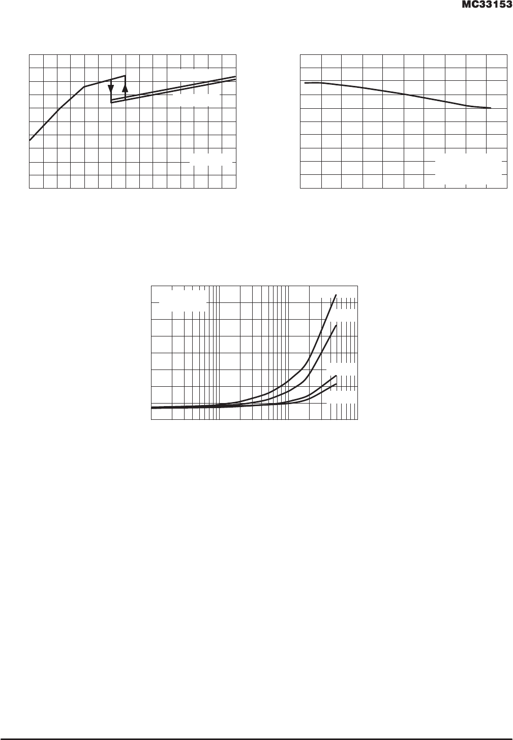
Figure 27. Supply Current versus
Supply Voltage
V
CC
, SUPPLY VOLTAGE (V)
Figure 28. Supply Current versus Temperature
Output High
Figure 29. Supply Current versus Input Frequency
Output Low
T
A
= 25°C
I
CC
, SUPPLY CURRENT (mA)
C
L
= 10 nF
= 5.0 nF
= 2.0 nF
= 1.0 nF
I
CC
, SUPPLY CURRENT (mA)
8.0
6.0
4.0
2.0
0 20 40 60 80 100 120 14020 –20
0
–4010 15
8.0
6.0
4.0
2.0
0
100010 100
60
40
20
0
OPERATING DESCRIPTION
GATE DRIVE
Controlling Switching Times
The most important design aspect of an IGBT gate drive is
optimization of the switching characteristics. The switching
characteristics are especially important in motor control
applications in which PWM transistors are used in a bridge
configuration. In these applications, the gate drive circuit
components should be selected to optimize turn–on, turn–off
and off–state impedance. A single resistor may be used to
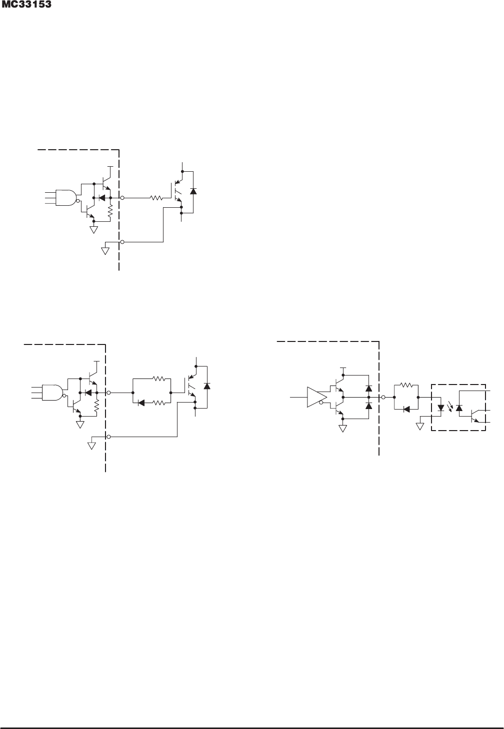
control both turn–on and turn–off as shown in Figure 30.
However, the resistor value selected must be a compromise
in turn–on abruptness and turn–off losses. Using a single
resistor is normally suitable only for very low frequency
PWM. An optimized gate drive output stage is shown in Fig-
ure 31. This circuit allows turn–on and turn–off to be opti-
mized separately. The turn–on resistor, R
on
, provides control
over the IGBT turn–on speed. In motor control circuits, the
resistor sets the turn–on di/dt that controls how fast the free–
wheel diode is cleared. The interaction of the IGBT and free–
wheeling diode determines the turn–on dv/dt. Excessive
turn–on dv/dt is a common problem in half–bridge circuits.
The turn–off resistor, R
off
, controls the turn–off speed and
ensures that the IGBT remains off under commutation
stresses. Turn–off is critical to obtain low switching losses.
While IGBTs exhibit a fixed minimum loss due to minority car-
rier recombination, a slow gate drive will dominate the turn–
off losses. This is particularly true for fast IGBTs. It is also
possible to turn–off an IGBT too fast. Excessive turn–off
speed will result in large overshoot voltages. Normally, the
turn–off resistor is a small fraction of the turn–on resistor.
The MC33153 contains a bipolar totem pole output stage
that is capable of sourcing 1.0 amp and sinking 2.0 amps
peak. This output also contains a pull down resistor to ensure
that the IGBT is off whenever there is insufficient V
CC
to the
MC33153.
In a PWM inverter, IGBTs are used in a half–bridge config-
uration. Thus, at least one device is always off. While the
IGBT is in the off–state, it will be subjected to changes in volt-
age caused by the other devices. This is particularly a prob-
lem when the opposite transistor turns on.
4–10
Motorola TMOS Power MOSFET Transistor Device Data
When the lower device is turned on, clearing the upper
diode, the turn–on dv/dt of the lower device appears across
the collector emitter of the upper device. To eliminate shoot–
through currents, it is necessary to provide a low sink imped-
ance to the device that is in the off–state. In most applications
the turn–off resistor can be made small enough to hold off the
device that is under commutation without causing exces-
sively fast turn–off speeds.
Figure 30. Using a Single Gate Resistor
Output
V
CC
V
EE
5
V
EE
V
EE
3
R
g
IGBT
Figure 31. Using Separate Resistors
for Turn–On and Turn–Off
Output
V
CC
V
EE
5
V
EE
V
EE
3
R
on
IGBT
R
off
D
off
A negative bias voltage can be used to drive the IGBT into
the off–state. This is a practice carried over from bipolar Dar-
lington drives and is generally not required for IGBTs. How-
ever, a negative bias will reduce the possibility of
shoot–through. The MC33153 has separate pins for V
EE
and
Kelvin Ground. This permits operation using a +15/–5.0 V
supply.
INTERFACING WITH OPTOISOLATORS
Isolated Input
The MC33153 may be used with an optically isolated
input. The optoisolator can be used to provide level shifting,
and if desired, isolation from ac line voltages. An optoisolator
with a very high dv/dt capability should be used, such as the
Hewlett Packard HCPL4053. The IGBT gate turn–on resistor
should be set large enough to ensure that the opto’s dv/dt
capability is not exceeded. Like most optoisolators, the
HCPL4053 has an active low open–collector output. Thus,
when the LED is on, the output will be low. The MC33153 has
an inverting input pin to interface directly with an optoisolator
using a pull up resistor. The input may also be interfaced
directly to 5.0 V CMOS logic or a microcontroller.
Optoisolator Output Fault
The MC33153 has an active high fault output. The fault
output may be easily interfaced to an optoisolator. While it is
important that all faults are properly reported, it is equally
important that no false signals are propagated. Again, a high
dv/dt optoisolator should be used.
The LED drive provides a resistor programmable current
of 10 to 20 mA when on, and provides a low impedance path
when off. An active high output, resistor, and small signal
diode provide an excellent LED driver. This circuit is shown in
Figure 32.
Figure 32. Output Fault Optoisolator
Short Circuit
Latch Output
7
V
EE
V
CC
V
EE
Q
UNDERVOLTAGE LOCKOUT
It is desirable to protect an IGBT from insufficient gate volt-
age. IGBTs require 15 V on the gate to achieve the rated on–
voltage. At gate voltages below 13 V, the on–voltage
increases dramatically, especially at higher currents. At very
low gate voltages, below 10 V, the IGBT may operate in the
linear region and quickly overheat. Many PWM motor drives
use a bootstrap supply for the upper gate drive. The UVLO
provides protection for the IGBT in case the bootstrap capac-
itor discharges.
The MC33153 will typically start up at about 12 V. The
UVLO circuit has about 1.0 V of hysteresis and will disable
the output if the supply voltage falls below about 11V.
4–11
Motorola TMOS Power MOSFET Transistor Device Data
PROTECTION CIRCUITRY
Desaturation Protection
Bipolar Power circuits have commonly used what is known
as “Desaturation Detection”. This involves monitoring the col-
lector voltage and turning off the device if this voltage rises
above a certain limit. A bipolar transistor will only conduct a
certain amount of current for a given base drive. When the
base is overdriven, the device is in saturation. When the col-
lector current rises above the knee, the device pulls out of
saturation. The maximum current the device will conduct in
the linear region is a function of the base current and the dc
current gain (h
FE
) of the transistor.
The output characteristics of an IGBT are similar to a Bipo-
lar device. However, the output current is a function of gate
voltage instead of current. The maximum current depends on
the gate voltage and the device type. IGBTs tend to have a
very high transconductance and a much higher current den-
sity under a short circuit than a bipolar device. Motor control
IGBTs are designed for a lower current density under shorted
conditions and a longer short circuit survival time.
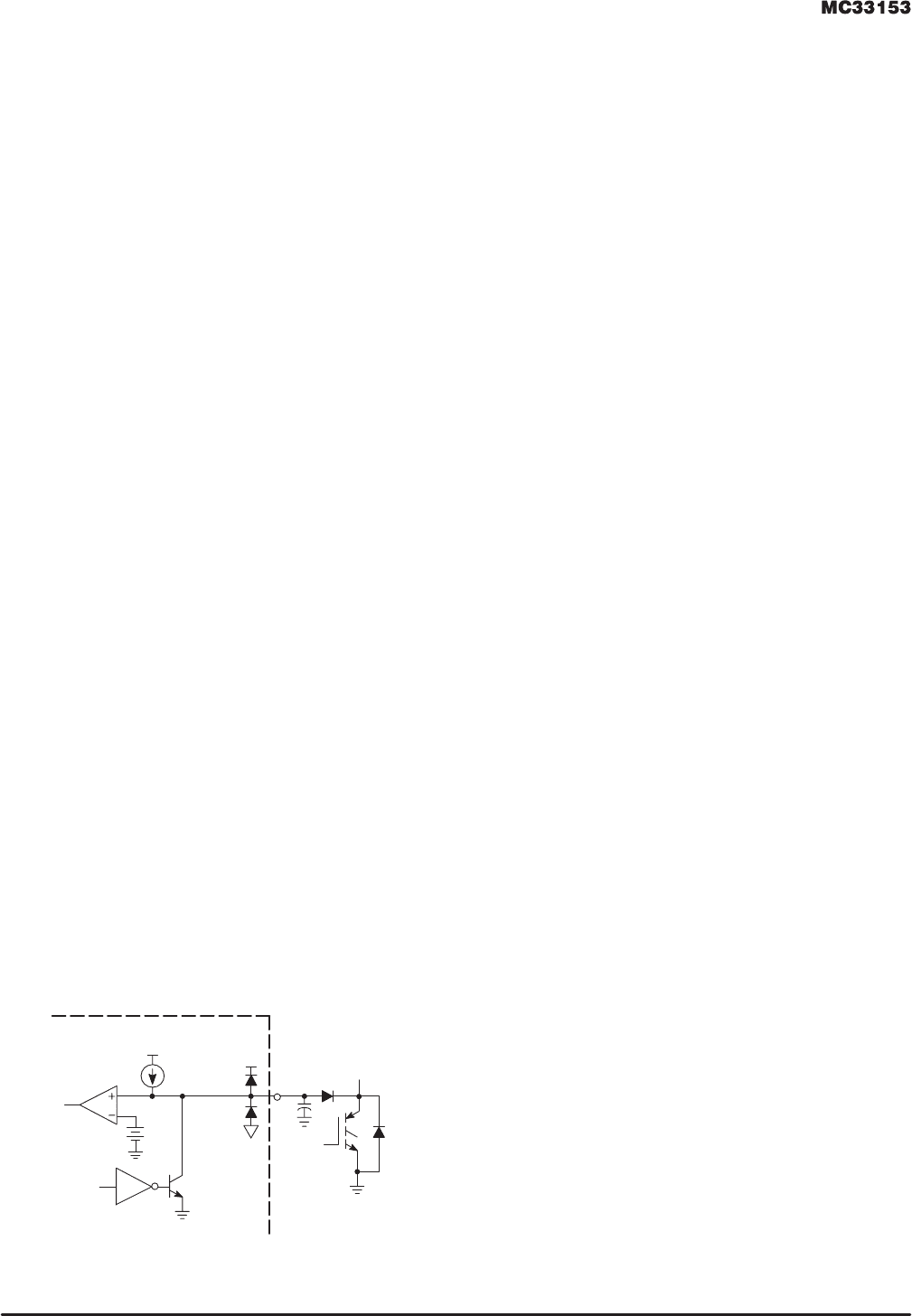
The best method for detecting desaturation is the use of a
high voltage clamp diode and a comparator. The MC33153
has a Fault Blanking/Desaturation Comparator which senses
the collector voltage and provides an output indicating when
the device is not fully saturated. Diode D1 is an external high
voltage diode with a rated voltage comparable to the power
device. When the IGBT is “on” and saturated, D1 will pull
down the voltage on the Fault Blanking/Desaturation Input.
When the IGBT pulls out of saturation or is “off”, the current
source will pull up the input and trip the comparator. The
comparator threshold is 6.5 V, allowing a maximum on–volt-
age of about 5.8 V.
A fault exists when the gate input is high and V
CE
is
greater than the maximum allowable V
CE(sat)
. The output of
the Desaturation Comparator is ANDed with the gate input
signal and fed into the Short Circuit and Overcurrent Latches.
The Overcurrent Latch will turn–off the IGBT for the remain-
der of the cycle when a fault is detected. When input goes
high, both latches are reset. The reference voltage is tied to
the Kelvin Ground instead of the V
EE
to make the threshold
independent of negative gate bias. Note that for proper
operation of the Desaturation Comparator and the Fault Out-
put, the Current Sense Input must be biased above the Over-
current and Short Circuit Comparator thresholds. This can be
accomplished by connecting Pin 1 to V
CC
.
Figure 33. Desaturation Detection
V
CC
V
EE
V
CC
8
270 µA
V
ref
6.5 V
Desaturation
Comparator
Kelvin
Gnd
D1
The MC33153 also features a programmable fault blank-
ing time. During turn–on, the IGBT must clear the opposing
free–wheeling diode. The collector voltage will remain high
until the diode is cleared. Once the diode has been cleared,
the voltage will come down quickly to the V
CE(sat)
of the
device. Following turn–on, there is normally considerable
ringing on the collector due to the C
OSS
capacitance of the
IGBTs and the parasitic wiring inductance. The fault signal
from the Desaturation Comparator must be blanked suffi-
ciently to allow the diode to be cleared and the ringing to
settle out.
The blanking function uses an NPN transistor to clamp the
comparator input when the gate input is low. When the input
is switched high, the clamp transistor will turn “off”, allowing
the internal current source to charge the blanking capacitor.
The time required for the blanking capacitor to charge up
from the on–voltage of the internal NPN transistor to the trip
voltage of the comparator is the blanking time.
If a short circuit occurs after the IGBT is turned on and sat-
urated, the delay time will be the time required for the current
source to charge up the blanking capacitor from the V
CE(sat)
level of the IGBT to the trip voltage of the comparator. Fault
blanking can be disabled by leaving Pin 8 unconnected.
Sense IGBT Protection
Another approach to protecting the IGBTs is to sense the
emitter current using a current shunt or Sense IGBTs. This
method has the advantage of being able to use high gain
IGBTs which do not have any inherent short circuit capability.
Current sense IGBTs work as well as current sense MOS-
FETs in most circumstances. However, the basic problem of
working with very low sense voltages still exists. Sense
IGBTs sense current through the channel and are therefore
linear with respect to the collector current. Because IGBTs
have a very low incremental on–resistance, sense IGBTs
behave much like low–on resistance current sense MOS-
FETs. The output voltage of a properly terminated sense
IGBT is very low, normally less than 100 mV.
The sense IGBT approach requires fault blanking to pre-
vent false tripping during turn–on. The sense IGBT also
requires that the sense signal is ignored while the gate is low.
This is because the mirror output normally produces large
transient voltages during both turn–on and turn–off due to the
collector to mirror capacitance. With non–sensing types of
IGBTs, a low resistance current shunt (5.0 to 50 mΩ) can be
used to sense the emitter current. When the output is an
actual short circuit, the inductance will be very low. Since the
blanking circuit provides a fixed minimum on–time, the peak
current under a short circuit can be very high. A short circuit
discern function is implemented by the second comparator
which has a higher trip voltage. The short circuit signal is
latched and appears at the Fault Output. When a short circuit
is detected, the IGBT should be turned–off for several milli-
seconds allowing it to cool down before it is turned back on.
The sense circuit is very similar to the desaturation circuit. It
is possible to build a combination circuit that provides protec-
tion for both Short Circuit capable IGBTs and Sense IGBTs.

4–12
Motorola TMOS Power MOSFET Transistor Device Data
APPLICATION INFORMATION
Figure 34 shows a basic IGBT driver application. When
driven from an optoisolator, an input pull up resistor is
required. This resistor value should be set to bias the output
transistor at the desired current. A decoupling capacitor
should be placed close to the IC to minimize switching noise.
A bootstrap diode may be used for a floating supply. If the
protection features are not required, then both the Fault
Blanking/Desaturation and Current Sense Inputs should both
be connected to the Kelvin Ground (Pin 2). When used with a
single supply, the Kelvin Ground and V
EE
pins should be con-
nected together. Separate gate resistors are recommended
to optimize the turn–on and turn–off drive.
Figure 34. Basic Application
7
4
3
2
1
5
8
6
Fault
Input
Desat/
Blank
Output
Sense
Gnd
V
EE
V
CC
MC33153
+18 V
B+
Bootstrap
Figure 35. Dual Supply Application
7
4
3
2
1
5
8
6
Fault
Input
Desat/
Blank
Output
Sense
Gnd
V
EE
V
CC
MC33153
+15 V
–5.0 V
When used in a dual supply application as in Figure 35, the
Kelvin Ground should be connected to the emitter of the
IGBT. If the protection features are not used, then both the
Fault Blanking/Desaturation and the Current Sense Inputs
should be connected to Ground. The input optoisolator
should always be referenced to V
EE
.
If desaturation protection is desired, a high voltage diode
is connected to the Fault Blanking/Desaturation pin. The
blanking capacitor should be connected from the Desatura-
tion pin to the V
EE
pin. If a dual supply is used, the blanking
capacitor should be connected to the Kelvin Ground. The
Current Sense Input should be tied high because the two
comparator outputs are ANDed together. Although the
reverse voltage on collector of the IGBT is clamped to the
emitter by the free–wheeling diode, there is normally consid-
erable inductance within the package itself. A small resistor
in series with the diode can be used to protect the IC from
reverse voltage transients.
Figure 36. Desaturation Application
7
4
3
2
1
5
8
6
Fault
Input
Desat/
Blank
Output
Sense
Gnd
V
EE
V
CC
MC33153
+18 V
C
Blank
When using sense IGBTs or a sense resistor, the sense
voltage is applied to the Current Sense Input. The sense trip
voltages are referenced to the Kelvin Ground pin. The sense
voltage is very small, typically about 65 mV, and sensitive to
noise. Therefore, the sense and ground return conductors
should be routed as a differential pair. An RC filter is useful in
filtering any high frequency noise. A blanking capacitor is
connected from the blanking pin to V
EE
. The stray capaci-
tance on the blanking pin provides a very small level of blank-
ing if left open. The blanking pin should not be grounded
when using current sensing, that would disable the sense.
The blanking pin should never be tied high, that would short
out the clamp transistor.
Figure 37. Sense IGBT Application
7
4
3
2
1
5
8
6
Fault
Input
Desat/
Blank
Output
Sense
Gnd
V
EE
V
CC
MC33153
+18 V

4–13
Motorola TMOS Power MOSFET Transistor Device Data
This Logic Level Insulated Gate Bipolar Transistor (IGBT)
features Gate–Emitter ESD protection, Gate–Collector overvoltage
protection from SMARTDISCRETES monolithic circuitry for
usage as an Ignition Coil Driver.
• Temperature Compensated Gate–Drain Clamp Limits Stress
Applied to Load
• Integrated ESD Diode Protection
• Low Threshold Voltage to Interface Power Loads to Logic or
Microprocessors
• Low Saturation Voltage
• High Pulsed Current Capability
MAXIMUM RATINGS
(T
J
= 25°C unless otherwise noted)
Rating Symbol Value Unit
Collector–Emitter Voltage V
CES
CLAMPED Vdc
Collector–Gate Voltage V
CGR
CLAMPED Vdc
Gate–Emitter Voltage V
GE
CLAMPED Vdc
Collector Current — Continuous @ T
C
= 25°C
Collector Current — Single Pulsed (t
p
= 10 s)
I
C
I
CM
20
60
Adc
Apk
Total Power Dissipation @ T
C
= 25°C (TO–220)
Derate Above 25°C
P
D
150
1.0
Watts
W/°C
Operating and Storage Temperature Range T
J
, T
stg
–55 to 175 °C
Single Pulse Collector–Emitter Avalanche Energy @ Starting T
J
= 25°C
(V
CC
= 80 V, V
GE
= 5 V, Peak I
L
= 10 A, L = 10 mH)
E
AS
500
mJ
THERMAL CHARACTERISTICS
Thermal Resistance — Junction to Case – (TO–220)
Thermal Resistance — Junction to Ambient
R
JC
R
JA
1.0
62.5
°C/W
Maximum Lead Temperature for Soldering Purposes, 1/8″ from case for 5 seconds T
L
275 °C
Mounting Torque, 6–32 or M3 screw
10 lbf in (1.13 N m)
This document contains information on a new product. Specifications and information herein are subject to change without notice.
SEMICONDUCTOR TECHNICAL DATA
20 AMPERES
VOLTAGE CLAMPED
N–CHANNEL IGBT
V
ce(on)
= 1.9 VOLTS
135 VOLTS (CLAMPED)
CASE 221A–06, Style 9
TO–220AB
G
C
E
C
G
E
Rge
4–14
Motorola TMOS Power MOSFET Transistor Device Data
ELECTRICAL CHARACTERISTICS
(T
C
= 25°C unless otherwise noted)
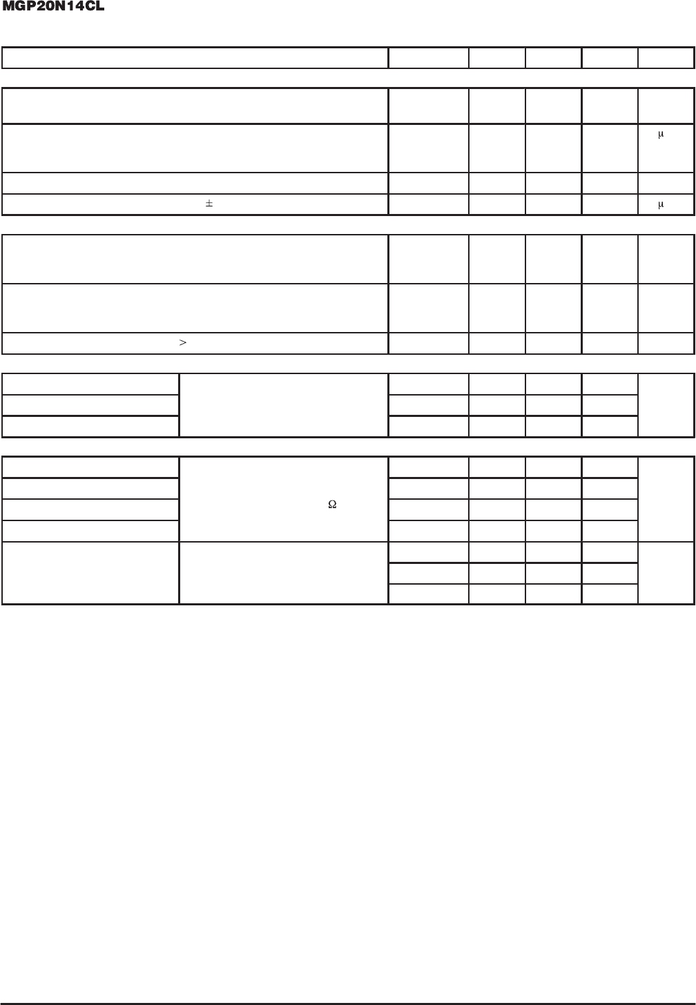
Characteristic Symbol Min Typ Max Unit
OFF CHARACTERISTICS
Clamp Voltage
(I
Clamp
= 10 mA, T
J
= –40 to 150°C)
B
VCES
135
Vdc
Zero Gate Voltage Collector Current
(V
CE
= 100 V, V
GE
= 0 V)
(V
CE
= 100 V, V
GE
= 0 V, T
J
= 150°C)
I
CES
—
—
—
—
10
100
A
Gate–Emitter Clamp Voltage (I
G
= 1 mA) B
VGES
10 Vdc
Gate–Emitter Leakage Current (V
GE
= 5 V, V
CE
= 0 V) I
GES
— — 1.0
A
ON CHARACTERISTICS (1)
Gate Threshold Voltage
(V
CE
= V
GE
, I
C
= 1 mA)
Threshold Temperature Coefficient (Negative)
V
CE(th)
1.0 1.5
4.4
2.0
V
mV/°C
Collector–Emitter On–Voltage
(V
GE
= 5 V, I
C
= 10 A)
(V
GE
= 5 V, I
C
= 10 Adc, T
J
= 175°C)
V
CE(on)
—
—
1.9
1.8
V
Forward Transconductance (V
CE
15 V, I
C
= 10 A) g
fs
8.0 15 — Mhos
DYNAMIC CHARACTERISTICS
Input Capacitance
(V 25 Vd V 0 Vd
C
iss
— 430 600
pF
Output Capacitance
(V
CE
= 25 Vdc, V
GE
= 0 Vdc,
f = 1.0 MHz
)
C
oss
— 182 250
Transfer Capacitance
f
1.0
MHz)
C
rss
— 48 100
SWITCHING CHARACTERISTICS (1)
Turn–On Delay Time t
d(on)
— TBD TBD
ns
Rise Time
(V
CC
= 68 V, I
C
= 20 A,
t
r
— TBD TBD
Turn–Off Delay Time
(
CC C
V
GE
= 5 V, R
G
= 9.1 )
t
d(off)
— TBD TBD
Fall Time t
f
— TBD TBD
Total Gate Charge
(V 108 V I 20 A
Q
g
— 14 20
nC
Gate–Emitter Charge
(V
CC
= 108 V, I
C
= 20 A,
V
GE
= 5 V
)
Q
gs
— 3.0 —
Gate–Collector Charge
V
GE
5
V)
Q
gd
— 6.0 —
(1) Pulse Test: Pulse Width ≤ 300 µs, Duty Cycle ≤ 2%.

4–15
Motorola TMOS Power MOSFET Transistor Device Data
This Logic Level Insulated Gate Bipolar Transistor (IGBT)
features Gate–Emitter ESD protection, Gate–Collector overvoltage
protection from SMARTDISCRETES monolithic circuitry for
usage as an Ignition Coil Driver.
• Temperature Compensated Gate–Drain Clamp Limits Stress
Applied to Load
• Integrated ESD Diode Protection
• Low Threshold Voltage to Interface Power Loads to Logic or
Microprocessors
• Low Saturation Voltage
• High Pulsed Current Capability
MAXIMUM RATINGS
(T
J
= 25°C unless otherwise noted)
Rating Symbol Value Unit
Collector–Emitter Voltage V
CES
CLAMPED Vdc
Collector–Gate Voltage V
CGR
CLAMPED Vdc
Gate–Emitter Voltage V
GE
CLAMPED Vdc
Collector Current — Continuous @ T
C
= 25°C I
C
20 Adc
Reversed Collector Current – pulse width 100 s
I
CR
12 Apk
Total Power Dissipation @ T
C
= 25°C (TO–220) P
D
150 Watts
Electrostatic Voltage — Gate–Emitter ESD 3.5 kV
Operating and Storage Temperature Range T
J
, T
stg
–55 to 175 °C
THERMAL CHARACTERISTICS
Thermal Resistance — Junction to Case – (TO–220)
Thermal Resistance — Junction to Ambient
R
JC
R
JA
1.0
62.5
°C/W
Maximum Lead Temperature for Soldering Purposes, 1/8″ from case for 5 seconds T
L
275 °C
Mounting Torque, 6–32 or M3 screw
10 lbf in (1.13 N m)
UNCLAMPED INDUCTIVE SWITCHING CHARACTERISTICS
Single Pulse Collector–Emitter Avalanche Energy
@ Starting T
J
= 25°C
@ Starting T
J
= 150°C
E
AS
550
150
mJ
This document contains information on a new product. Specifications and information herein are subject to change without notice.
SEMICONDUCTOR TECHNICAL DATA
20 AMPERES
VOLTAGE CLAMPED
N–CHANNEL IGBT
V
ce(on)
= 1.8 VOLTS
350 VOLTS (CLAMPED)
CASE 221A–06, Style 9
TO–220AB
G
C
E
C
G
E
Rge
4–16
Motorola TMOS Power MOSFET Transistor Device Data
ELECTRICAL CHARACTERISTICS
(T
C
= 25°C unless otherwise noted)
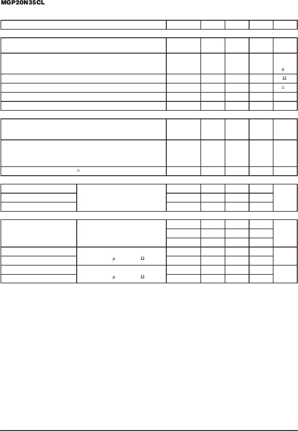
Characteristic Symbol Min Typ Max Unit
OFF CHARACTERISTICS
Collector–to–Emitter Breakdown Voltage
(I
Clamp
= 10 mA, T
J
= –40 to 150°C)
B
VCES
320 350 380
Vdc
Zero Gate Voltage Collector Current
(V
CE
= 250 V, V
GE
= 0 V, T
J
= 125°C)
(V
CE
= 15 V, V
GE
= 0 V, T
J
= 125°C)
I
CES
—
—
—
—
1.0
200
mA
A
Resistance Gate–Emitter (T
J
= –40 to 150°C) R
GE
10k 16k 30k
Gate–Emitter Breakdown Voltage (I
G
= 2 mA) B
VGES
11 13 15 V
Collector–Emitter Reverse Leakage (V
CE
= –15 V, T
J
= –40 to 150°C) I
CES
— 8 100 mA
Collector–Emitter Reversed Breakdown Voltage (I
E
= 75 mA) B
VCER
26 40 120 V
ON CHARACTERISTICS (1)
Gate Threshold Voltage
(V
CE
= V
GE
, I
C
= 1 mA)
(V
CE
= V
GE
, I
C
= 1 mA, T
J
= 150°C)
V
GE(th)
1.0
0.75
1.7
—
2.4
1.8
V
Collector–Emitter On–Voltage
(V
GE
= 5 V, I
C
= 5 A)
(V
GE
= 5 V, I
C
= 10 A)
(V
GE
= 5 V, I
C
= 10 Adc, T
J
= 150°C)
V
CE(on)
—
—
—
1.1
1.4
1.4
1.4
1.9
1.8
V
Forward Transconductance (V
CE
50 V, I
C
= 10 A) g
fs
10 16 — S
DYNAMIC CHARACTERISTICS
Input Capacitance
(V 25 Vd V 0 Vd
C
iss
— 2800 —
pF
Output Capacitance
(V
CE
= 25 Vdc, V
GE
= 0 Vdc,
f = 1.0 MHz
)
C
oss
— 200 —
Transfer Capacitance
f
1.0
MHz)
C
rss
— 25 —
SWITCHING CHARACTERISTICS (1)
Total Gate Charge
(V 280 V I 20 A
Q
g
— 45 80
nC
Gate–Emitter Charge
(V
CC
= 280 V, I
C
= 20 A,
V
GE
= 5 V
)
Q
gs
— 8.0 —
Gate–Collector Charge
V
GE
5
V)
Q
gd
— 20 —
Turn–Off Delay Time
(V
CC
= 320 V, I
C
= 20 A,
t
d(off)
— TBD TBD
µs
Fall Time
(
CC C
L = 200 H, R
G
= 1 K )
t
f
— TBD TBD
Turn–On Delay Time
(V
CC
= 14 V, I
C
= 20 A,
t
d(on)
— TBD TBD µs
Rise Time
(
CC C
L = 200 H, R
G
= 1 K )
t
r
— TBD TBD
(1) Pulse Test: Pulse Width ≤ 300 µs, Duty Cycle ≤ 2%.

4–17
Motorola TMOS Power MOSFET Transistor Device Data
TYPICAL ELECTRICAL CHARACTERISTICS
Figure 1. Output Characteristics, T
J
= 25°C Figure 2. Output Characteristics, T
J
= 125°C
V
CE
, COLLECTOR–TO–EMITTER VOLTAGE (VOLTS)
I
C
, COLLECTOR CURRENT (AMPS)
I
C
, COLLECTOR CURRENT (AMPS)
V
CE
, COLLECTOR–TO–EMITTER VOLTAGE (VOLTS)
T
J
= 25°C
V
GE
= 10 V T
J
= 125°C
0123 8
20
10
0
30
4
0
4567024 68
4
0
30
20
10
0
3 V
Figure 3. Transfer Characteristics Figure 4. Collector–to–Emitter Saturation
Voltage versus Junction Temperature
V
GE
, GATE–TO–EMITTER VOLTAGE (VOLTS)
I
C
, COLLECTOR CURRENT (AMPS)
V
CE
, COLLECTOR–TO–EMITTER VOLTAGE (VOLTS)
T
J
, JUNCTION TEMPERATURE (°C)
T
J
= 125°C
V
GE
= 5 V
–50 0 150
1.8
1.4
1.2
1.0
1.6
2.0
2.2
50 10012345
40
30
20
10
0
Figure 5. Capacitance Variation Figure 6. High Voltage Capacitance Variation
COLLECTOR–TO–EMITTER VOLTAGE (VOLTS)
C, CAPACITANCE (pF)
DRAIN–TO–SOURCE VOLTAGE (VOLTS)
10
1000
10
1.0
100
1000
10005075
10000
1000
100
10
1.0
10 9 10
25 100 125 150 175 200
C, CAPACITANCE (pF)
V
GE
= 10 V
5 V
4 V
3 V
5 V
4 V
25°C
V
CE
= 10 V
I
C
= 20 A
15 A
10 A
T
J
= 25°C
V
CE
= 0 V
T
J
= 25°C
V
CE
= 0 V
C
iss
C
oss
C
rss
C
iss
C
oss
C
rss
