Справочник по мощным TMOS транзисторам (MOTOROLA)
Подождите немного. Документ загружается.

Introduction and Basic Characteristics
3–8
Motorola TMOS Power MOSFET Transistor Device Data
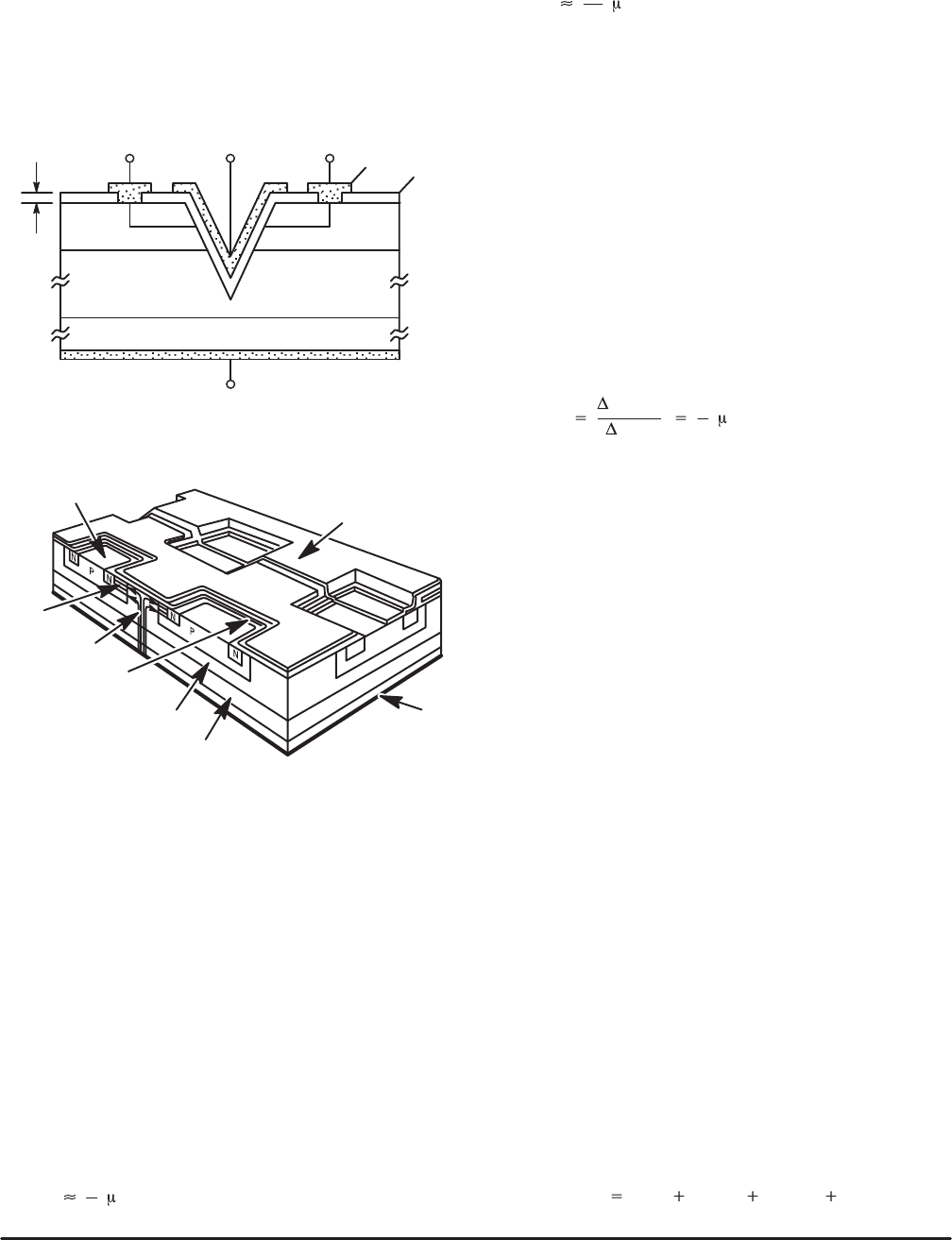
The cell structure chosen for Motorola’s TMOS power
MOSFET’s is shown in Figure 1–6. This structure is similar to
that of Figure 1–4 except that the drain contact is dropped
through the N
–
substrate to the back of the die. The gate
structure is now made with polysilicon sandwiched between
two oxide layers and the source metal applied continuously
over the entire active area. This two layer electrical contact
gives the optimum in packing density and maintains the
processing advantages of planar LDMOS. This results in a
highly manufacturable process which yields low R
DS(on)
and
high voltage product.
Figure 1–5. V–Groove MOSFET Structure Has
Short Vertical Channels with Low
Drain–to–Source Resistance
X
of
n +
A1
SiO
2
D
SG
p
n –
n +
S
Figure 1–6. TMOS Power MOSFET Structure Offers
Vertical Current Flow, Low Resistance Paths and
Permits Compact Metalization on Top and Bottom
Surfaces to Reduce Chip Size
SOURCE SITE
N–CHANNEL
DRAIN CURRENT
INSULATING OXIDE, SiO
2
N–SUBSTRATE
N–Epi LAYER
DRAIN
METALIZATION
SOURCE
METALIZATION
SILICON
GATE
Operation:
Transistor action and the primary electrical parameters of
Motorola’s TMOS power MOSFET can be defined as follows:
Drain Current, I
D
:
When a gate voltage of appropriate polarity and magnitude
is applied to the gate terminal, the polysilicon gate induces
an inversion layer at the surface of the diffused channel
region represented by r
CH
in Figure 1–7 (page A–8). This
inversion layer or channel connects the source to the lightly
doped region of the drain and current begins to flow. For
small values of applied drain–to–source voltage, V
DS
, drain
current increases linearly and can be represented by Equa-
tion (1).
(1) I
D
Z
L
Co [V
GS
–V
GS(th)
]V
DS
As the drain voltage is increased, the drain current satu-
rates and becomes proportional to the square of the applied
gate–to–source voltage, V
GS
, as indicated in Equation (2).
(2) I
D
Z
2L
Co [V
GS
–V
GS(th)
]
2
Where µ = Carrier Mobility
Co
Z
L
= Gate Oxide Capacitance per unit area
= Channel Width
= Channel Length
These values are selected by the device design engineer
to meet design requirements and may be used in modeling
and circuit simulations. They explain the shape of the output
characteristics discussed in Chapter 2.
Transconductance, g
FS
:
The transconductance or gain of the TMOS power
MOSFET is defined as the ratio of the change in drain cur-
rent and an accompanying small change in applied gate–to–
source voltage and is represented by Equation (3).
(3) g
FS
I
D(sat)
V
GS
Z
L
Co [V
GS
–V
GS(th)
]
The parameters are the same as above and demonstrate
that drain current and transconductance are directly related
and are a function of the die design. Note that transconduc-
tance is a linear function of the gate voltage, an important
feature in amplifier design.
Threshold Voltage, V
GS(th)
Threshold voltage is the gate–to–source voltage required
to achieve surface inversion of the diffused channel region,
(r
CH
in Figure 1–7) and as a result, conduction in the
channel.
As the gate voltage increases the more the channel is
“enhanced,” or the lower its resistance (r
CH
) is made, the
more current will flow. Threshold voltage is measured at a
specified value of current to maintain measurement correla-
tions. A value of 1.0 mA is common throughout the industry.
This value is primarily a function of the gate oxide thickness
and channel doping level which are chosen during the die
design to give a high enough value to keep the device off with
no bias on the gate at high temperatures. A minimum value
of 1.5 volts at room temperature will guarantee the transistor
remains an enhancement mode device at junction tempera-
tures up to 150°C.
On–Resistance, R
DS(on)
:
On–resistance is defined as the total resistance encoun-
tered by the drain current as it flows from the drain terminal to
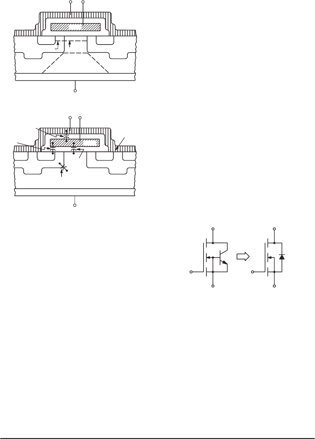
the source terminal. Referring to Figure 1–7, R
DS(on)
is com-
posed primarily of four resistive components associated with:
The Inversion channel, r
CH
; the Gate–Drain Accumulation
Region, r
ACC
; the junction FET Pinch region, r
JFET
; and the
lightly doped Drain Region, r
D
, as indicated in Equation (4).
(4) R
DS(on)
r
CH
r
ACC
r
JFET
r
D
3–9
Introduction and Basic CharacteristicsMotorola TMOS Power MOSFET Transistors Device Data
Figure 1–7. TMOS Device On–Resistance
P+
D
SG
P+
N +
N +
N –
POLY
N+
r
D
r
JFET
r
CH
r
ACC
Figure 1–8. TMOS Device Parasitic Capacitances
n +
P+
C
ds
D
SG
C
gs
P+
N +
N +
N +
N –
POLY
C
gd
A
C
gs
Whereas the channel resistance increases with channel
length, the accumulation resistance increases with poly
width and the JFET pinch resistance increases with epi
resistivity and all three are inversely proportional to the chan-
nel width and gate–to–source voltage. The drain resistance
is proportional to the epi resistivity, poly width and inversely
proportional to channel width. This says that the on–resis-
tance of TMOS power FETs with the thick and high resistivity
epi required for high voltage parts will be dominated by r
D
.
Low voltage devices have thin, low resistivity epi and r
CH
will be a large portion of the total on–resistance. This is
why high voltage devices are “full on” with moderate voltages
on the gate, whereas with low voltage devices the on–
resistance continues to decrease as V
GS
is increased toward
the maximum rating of the device.
Note: R
DS(on)
is inversely proportional to the carrier mobility. This
means that the R
DS(on)
of the P–Channel MOSFET is approximately
2.5 to 3.0 times that of a similar N–Channel MOSFET. Therefore, in
order to have matched complementary on characteristics, the Z/L ratio
of the P–Channel device must be 2.5–3.0 times that of the N–Channel
device. This means larger die are required for P–Channel MOSFET’s
with the same R
DS(on)
and same breakdown voltage as an N–Channel
device and thus device capacitances and costs will be
correspondingly higher.
Breakdown Voltage, V
(BR)DSS
:
Breakdown voltage or reverse blocking voltage of the
TMOS power MOSFET is defined in the same manner as
V
(BR)CES
in the bipolar transistor and occurs as an avalanche
breakdown. This voltage limit is reached when the carriers
within the depletion region of the reverse biased P–N junc-
tion acquire sufficient kinetic energy to cause ionization or
when the critical electric field is reached. The magnitude of
this voltage is determined mainly by the characteristics of the
lightly doped drain region and the type of termination of the
die’s surface electric field.
Figure 1–9 shows a schematic representation of the
cross–section in Figure 1–8 and depicts the bipolar transistor
built in the epi layer. Point A shows where the emitter and
base of the bipolar is shorted together. This is why V
(BR)DSS
of the power FET is equal to V
(BR)CES
of the bipolar. Also
note the short brings the base in contact with the source met-
al allowing the use of the base–collector junction. This is the
diode across the TMOS power MOSFET.
Figure 1–9. Schematic Diagram of all the Components
of the Cross Section of Figure 1–7
GG
SS
DD

Introduction and Basic Characteristics
3–10
Motorola TMOS Power MOSFET Transistor Device Data
TMOS Power MOSFET Capacitances:
Two types of intrinsic capacitances occur in the TMOS
power MOSFET – those associated with the MOS structure
and those associated with the P–N junction.
The two MOS capacitances associated with the MOSFET
cell are:
Gate–Source Capacitance, C
gs
Gate–Drain Capacitance, C
gd
The magnitude of each is determined by the die geometry
and the oxides associated with the silicon gate.
The P–N junction formed during fabrication of the power
MOSFET results in the drain–to–source capacitance, C
ds
.
This capacitance is defined the same as any other planar
junction capacitance and is a direct function of the channel
drain area and the width of the reverse biased junction deple-
tion region.
The dielectric insulator of C
gs
and C
gd
is basically a glass.
Thus these are very stable capacitors and will not vary with
voltage or temperature. If excessive voltage is placed on the
gate, breakdown will occur through the glass, creating a re-
sistive path and destroying MOSFET operation.
Optimizing TMOS Geometry:
The geometry and packing density of Motorola’s
MOSFETs vary according to the magnitude of the reverse
blocking voltage.
The geometry of the source site, as well as the spacing be-
tween source sites, represents important factors in efficient
power MOSFET design. Both parameters determine the
channel packing density, i.e.: ratio of channel width per cell to
cell area.
For low voltage devices, channel width is crucial for mini-
mizing R
DS(on)
, since the major contributing component of
R
DS(on)
is r
CH
. However, at high voltages, the major contrib-
uting component of resistance is r
D
and thus minimizing
R
DS(on)
is dependent on maximizing the ratio of active drain
area per cell to cell area. These two conditions for minimizing
R
DS(on)
cannot be met by a single geometry pattern for both
low and high voltage devices.
Distinct Advantages of Power MOSFETs
Power MOSFETs offer unique characteristics and capabili-
ties that are not available with bipolar power transistors. By
taking advantage of these differences, overall systems cost
savings can result without sacrificing reliability.
Speed
Power MOSFETs are majority carrier devices, therefore
their switching speeds are inherently faster. Without the
minority carrier stored base charge common in bipolar tran-
sistors, storage time is eliminated. The high switching
speeds allow efficient switching at higher frequencies which
reduces the cost, size and weight of reactive components.
MOSFET switching speeds are primarily dependent on
charging and discharging the device capacitances and are
essentially independent of operating temperature.
Input Characteristics
The gate of a power MOSFET is electrically isolated from
the source by an oxide layer that represents a dc resistance
greater than 40 megohms. The devices are fully biased–on
with a gate voltage of 10 volts. This significantly simplifies the
drive circuits and in many instances the gate may be driven
directly from logic integrated circuits such as CMOS and TTL
to control high power circuits directly.
Since the gate is isolated from the source, the drive
requirements are nearly independent of the load current.
This reduces the complexity of the drive circuit and results in
overall system cost reduction.
Safe Operating Area
Power MOSFETs, unlike bipolars, do not require derating
of power handling capability as a function of applied voltage.
The phenomena of second breakdown does not occur within
the ratings of the device. Depending on the application,
snubber circuits may be eliminated or a smaller capacitance
value may be used in the snubber circuit. The safe operating
boundaries are limited by the peak current ratings, break-
down voltages and the power capabilities of the devices.
On–Voltage
The minimum on–voltage of a power MOSFET is deter-
mined by the device on–resistance R
DS(on)
. For low voltage
devices the value of R
DS(on)
is extremely low, but with high
voltage devices the value increases. R
DS(on)
has a positive
temperature coefficient which aids in paralleling devices.
Examples of Advantages Offered by
MOSFETs
High Voltage Flyback Converter
An obvious way of showing the advantages of power
MOSFETs over bipolars is to compare the two devices in the
same system. Since the drive requirements are not the
same, it is not a question of simply replacing the bipolar with
the FET, but one of designing the respective drive circuits to
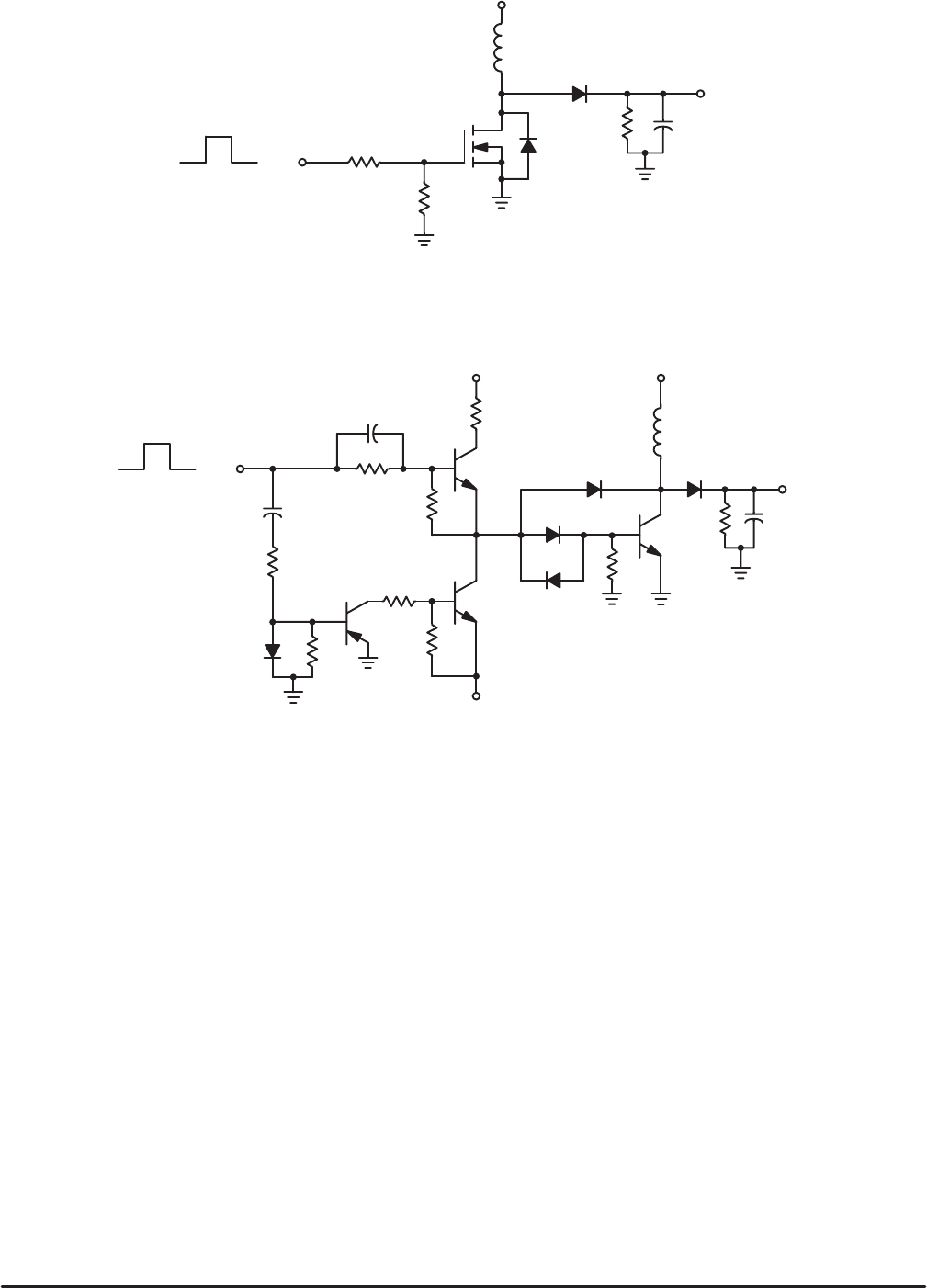
produce an equivalent output, as described in Figures 1–10
and 1–11.
For this application, a peak output voltage of about 700 V
driving a 30 kΩ load (P
O(pk)
≈ 16 W) was required. With the
component values and timing shown, the inductor/device
current required to generate this flyback voltage would have
to ramp up to about 3.0 A.
3–11
Introduction and Basic CharacteristicsMotorola TMOS Power MOSFET Transistors Device Data
Figure 1–10. TMOS Output Stage
Figure 1–11. Bipolar Driver and Output Stage
Figures 1–10 and 1–11. Circuit Configurations for a TMOS and
Bipolar Output Stage of a High Voltage Flyback Converter
15 V
0
PW ≤ 350 µs
f = 1.7 kHz
68
1.0 k
MTP4N80E
Q1
+V
DD
≤ 36 V
1.6 mH L
1N4725
R
L
30 k
C
L
V
o
≤ 800 V
0.5 µF
V
I
0
0.01 µF
270
1N914
150 pF
82
180
27
Q2
100
Q3
MJ8505
–V
D3
D2
D1
+V
CC
≤ 32 V+V
2.2 Ω
2.0 W
MJE200
Q1
47
Q4
30 k
0.5 µF
V
o
≤ 700 V
2N2905
1.0 k
MJE200
Figure 1–10 shows the TMOS version. Because of its high
input impedance, the FET, an MTP4N80E, can be directly
driven from the pulse width modulator. However, the PWM
output should be about 15 volts in amplitude and for relative-
ly fast FET switching be capable of sourcing and sinking
100 mA. Thus, all that is required to drive the FET is a resis-
tor or two. The peak drain current of 3.2 A is within the
MTP4N80E pulsed current rating of 18.0 A (4.0 A continu-
ous), and the turn–off load line of 3.2 A, 700 V is well within
the Switching SOA (18.0 A/800 V) of the device. Thus, the
circuit demonstrates the advantages of TMOS:
• High input impedance
• Fast Switching
• No Second breakdown
Compare this circuit with the bipolar version of Figure
1–11.
To achieve the output voltage, using a high voltage Switch-
mode MJ8505 power transistor, requires a rather complex
drive circuit for generating the proper I
B1
and I
B2
. This circuit
uses three additional transistors (two of which are power
transistors), three Baker clamp diodes, eleven passive com-
ponents and a negative power supply for generating an off–
bias voltage. Also, the RBSOA capability of this device is
only 3.0 A at 900 V and 4.7 A at 800 V, values below the
18.0 A/800 V rating of the MOSFET. A detailed description of
these circuits is shown in Chapter 8, Switching Power
Supplies.
Introduction and Basic Characteristics
3–12
Motorola TMOS Power MOSFET Transistor Device Data
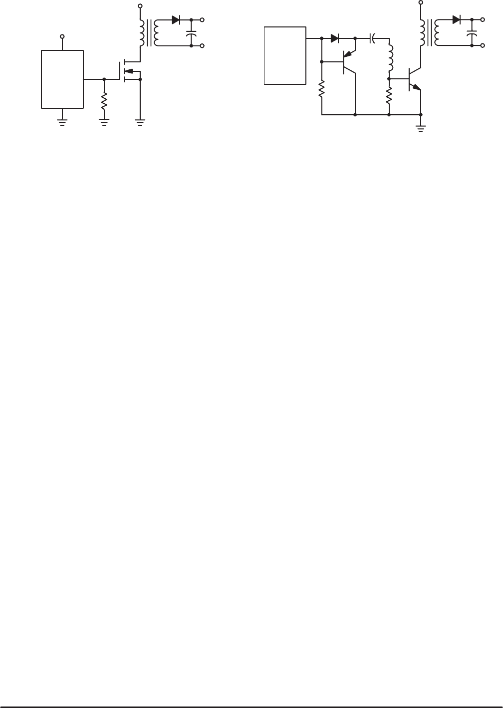
Figure 1–12. TMOS Version Figure 1–13. Bipolar Version
Figures 1–12 and 1–13. Comparison of Power MOSFET and Bipolar
in the Power Output Stage of a 20 kHz Switcher
MC3406
PWM
V
CC
+170 V
56
Q1
MTP4N50E
MC34060
1N4933
+10 µF
Q1 10 µH
47
MPSA55
200
+170 V
Q2
MJE13005
20 kHz Switcher
An example of MOSFET advantage over bipolar that illus-
trates its superior switching speed is shown in the power out-
put section of Figures 1–12 and 1–13. In addition to the drive
simplicity and reduced component count, the faster switching
speed offers better circuit efficiency. For this 35 W switching
regulator, using the same small heatsink for either device, a
case temperature rise of only 18°C was measured for the
MTP4N50E power MOSFET compared to a 46°C rise for the
MJE13005 bipolar transistor. Although the saturation losses
were greater for the TMOS, its lower switching losses pre-
dominated, resulting in a more efficient switching device.
In general, at low switching frequencies, where static
losses predominate, bipolars are more efficient. At higher
frequencies, above 50 kHz, the power MOSFETs are more
efficient.
3–13
Introduction and Basic CharacteristicsMotorola TMOS Power MOSFET Transistors Device Data
Chapter 2: Basic Characteristics of Power MOSFETs
Output Characteristics
Perhaps the most direct way to become familiar with the
basic operation of a device is to study its output characteris-
tics. In this case, a comparison of the MOSFET characteris-
tics with those of a bipolar transistor with similar ratings is in
order, since the curves of a bipolar device are almost univer-
sally familiar to power circuit design engineers.
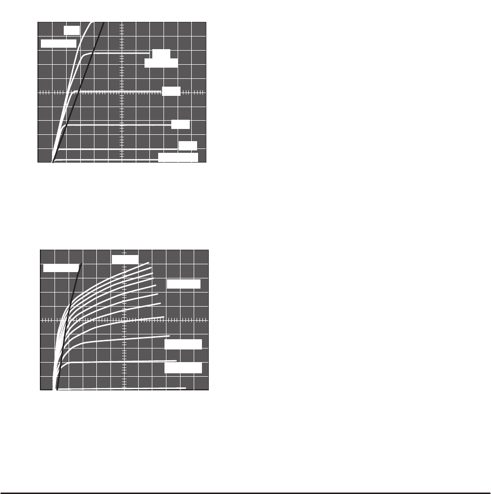
As indicated in Figures 2–1 and 2–2, the output character-
istics of the power MOSFET and the bipolar transistor can be
divided similarly into two basic regions. The figures also
show the numerous and often confusing terms assigned to
those regions. To avoid possible confusion, this section will
refer to the MOSFET regions as the “on” (or “ohmic”) and
“active” regions and bipolar regions as the “saturation” and
“active” regions.
Figure 2–1. I
D
–V
DS
Output Characteristics of a Power
MOSFET. Region A is Called the Ohmic, On, Constant
Resistance or Linear Region. Region B is Called the
Active, Constant Current, or Saturation Region.
10
9.0
8.0
7.0
6.0
5.0
4.0
3.0
2.0
1.0
0
0 4.0 8.0 12 16
V
DS
, DRAIN–SOURCE VOLTAGE (VOLTS)
I
D
, DRAIN CURRENT (AMPS)
10 V
REGION A
9.0 V
REGION B
6.0 V
POWER MOSFET
V
GS
= 5.0 V
8.0 V
7.0 V
I
B
= 20 mA
I
B
= 10 mA
0 4.0 8.0 12 16
100 mA
REGION A
REGION B
Figure 2–2. I
C
–V
CE
Output Characteristics of a Bipolar
Power Transistor. Region A is the Saturation Region.
Region B is the Linear or Active Region.
V
CE
, COLLECTOR–EMITTER VOLTAGE (VOLTS)
BIPOLAR POWER TRANSISTOR
10
9.0
8.0
7.0
6.0
5.0
4.0
3.0
2.0
1.0
0
One of the three obvious differences between Figures 2–1
and 2–2 is the family of curves for the power MOSFET is
generated by changes in gate voltage and not by base cur-
rent variations. A second difference is the slope of the curve
in the bipolar saturation region is steeper than the slope in
the ohmic region of the power MOSFET indicating that the
on–resistance of the MOSFET is higher than the effective
on–resistance of the bipolar.
The third major difference between the output characteris-
tics is that in the active regions the slope of the bipolar curve
is steeper than the slope of the TMOS curve, making the
MOSFET a better constant current source. The limiting of I
D
is due to pinch–off occurring in the MOSFET channel.
Basic MOSFET Parameters
On–Resistance
The on–resistance, or R
DS(on)
, of a power MOSFET is an
important figure of merit because it determines the amount of
current the device can handle without excessive power dis-
sipation. When switching the MOSFET from off to on, the
drain–source resistance falls from a very high value to
R
DS(on)
, which is a relatively low value. To minimize R
DS(on)
the gate voltage should be large enough for a given drain
current to maintain operation in the ohmic region. Data
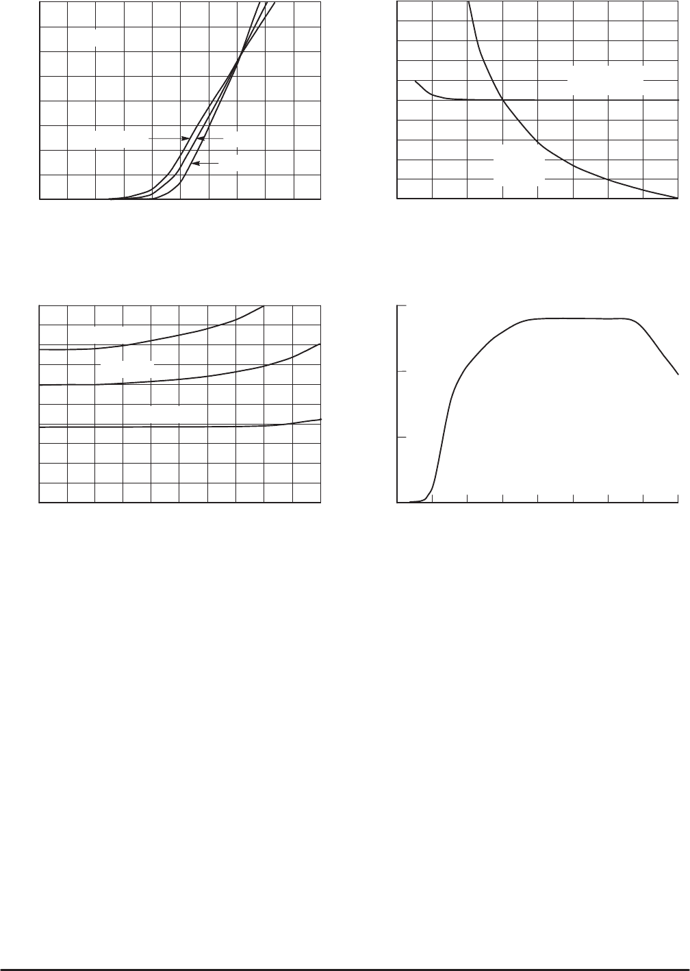
sheets usually include a graph, such as Figure 2–3, which
relates this information. As Figure 2–4 indicates, increasing
the gate voltage above 12 volts has a diminishing effect on
lowering on–resistance (especially in high voltage devices)
and increases the possibility of spurious gate–source voltage
spikes exceeding the maximum gate voltage rating of
20 volts. Somewhat like driving a bipolar transistor deep into
saturation, unnecessarily high gate voltages will increase
turn–off time because of the excess charge stored in the in-
put capacitance. All Motorola TMOS FETs will conduct the
rated continuous drain current with a gate voltage of 10 volts.
As the drain current rises, especially above the continuous
rating, the on–resistance also increases. Another important
relationship, which is addressed later with the other tempera-
ture dependent parameters, is the effect that temperature
has on the on–resistance. Increasing T
J
and I
D
both effect an
increase in R
DS(on)
as shown in Figure 2–5.
Transconductance
Since the transconductance, or g
FS
, denotes the gain of
the MOSFET, much like beta represents the gain of the bipo-
lar transistor, it is an important parameter when the device is
operated in the active, or constant current, region. Defined
as the ratio of the change in drain current corresponding to a
change in gate voltage (g
FS
= dI
D
/dV
GS
), the transconduc-
tance varies with operating conditions as seen in Figure 2–6.
The value of g
FS
is determined from the active portion of the
V
DS
–I
D
transfer characteristics where a change in V
DS
no
longer significantly influences g
FS
. Typically the transcon-
ductance rating is specified at half the rated continuous drain
current and at a V
DS
of 15 V.
Introduction and Basic Characteristics
3–14
Motorola TMOS Power MOSFET Transistor Device Data
V
DS
= 15 V
T
C
= 25°C
R
DS(on)
, DRAIN–TO–SOURCE RESISTANCE (OHMS)
0.5
0.4
0.3
0.2
0
0 5.0 10 15 20 25
T
J
= 100°C
0.1
1
.
25
4.0 6.0 8.0 10 12 20
HIGH VOLTAGE
MOSFET
1.20
1.15
1.10
1.05
1.00
0.95
0.90
0.85
0.80
0.75
14 16 18
LOW
VOLTAGE
MOSFET
NORMALIZED ON–RESISTANCE
I
D
, DRAIN CURRENT (AMPS)
8
.
0
6.0
4.0
2.0
0
0 2.0 4.0 6.0 8.0 10
V
DS
= 30 V
T
J
= 100°C
–55°C
25°C
Figure 2–3. Transfer Characteristics
V
GS
, GATE–TO–SOURCE VOLTAGE (VOLTS) V
GS
, GATE–TO–SOURCE VOLTAGE (VOLTS)
I
D
, DRAIN CURRENT (AMPS)
Figure 2–4. The Effect of Gate–to–Source
Voltage on On–Resistance Varies with a
Device’s Voltage Rating
Figure 2–5. Variation of R
DS(on)
with Drain
Current and Temperature
V
GS
, GATE–TO–SOURCE VOLTAGE (VOLTS)
Figure 2–6. Small–Signal Transconductance
versus V
GS
g
FS
, FORWARD TRANSCONDUCTANCE
(SIEMENS)
3.0
2.0
1.0
0
4.0 5.0 6.0 7.0 8.0 9.0 10 11 12
CURVE FALLS AS
DEVICE ENTERS
OHMIC REGION
(V
DS
DEPENDENT)
T
J
= 25°C
T
J
= 55°C
For designers interested only in switching the power
MOSFET between the on and off states, the transconduc-
tance is often an unused parameter. Obviously when the de-
vice is switched fully on, the transistor will be operating in its
ohmic region where the gate voltage will be high. In that re-
gion, a change in an already high gate voltage will do little to
increase the drain current; therefore, g
FS
is almost zero.
Threshold Voltage
Threshold Voltage, V
GS(th)
, is the lowest gate voltage at
which a specified small amount of drain current begins to
flow. Motorola normally specifies V
GS(th)
at an I
D
of one
milliampere. Device designers can control the value of the
threshold voltage and target V
GS(th)
to optimize device per-
formance and practicality. A low threshold voltage is desired
so the TMOS FET can be controlled by low voltage chips
such as CMOS and TTL. A low value also speeds switching
because less current needs to be transferred to charge the
parasitic input capacitances. But the threshold voltage can
be too low if noise can trigger the device. Also, a positive–
going voltage transient on the drain can be coupled to the
gate by the gate–to–drain parasitic capacitances and can
cause spurious turn–on of a device with a low V
GS(th)
.
Temperature Dependent Characteristics R
DS(on)
Junction temperature variations and their effect on the on–
resistance, R
DS(on)
, should be considered when designing
with power MOSFETs. Since R
DS(on)
varies approximately
linearly with temperature, power MOSFETs can be assigned
temperature coefficients that describe this relationship.
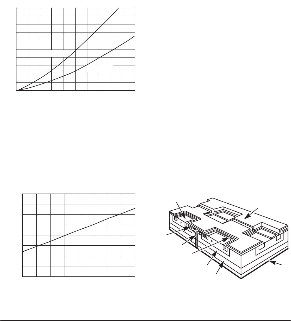
Figure 2–7 shows that the temperature coefficient of
R
DS(on)
is greater for high voltage devices than for low
voltage MOSFETs. A graph showing the variation of R
DS(on)
with junction temperature is shown on most data sheets, Fig-
ure 2–5.
Switching Speeds are Constant with Temperature
High junction temperatures emphasize one of the most de-
sirable characteristics of the MOSFET, that of low dynamic or
switching losses. In the bipolar transistor, temperature in-
creases will increase switching times, causing greater dy-
namic losses. On the other hand, thermal variations have
little effect on the switching speeds of the power MOSFET.
These speeds depend on how rapidly the parasitic input ca-
pacitances can be charged and discharged. Since the mag-
nitudes of these capacitances are essentially temperature
3–15
Introduction and Basic CharacteristicsMotorola TMOS Power MOSFET Transistors Device Data
invariant, so are the switching speeds. Therefore, as temper-
ature increases, the dynamic losses in a MOSFET are low
and remain constant, while in the bipolar transistors the
switching losses are higher and increase with junction tem-
perature.
Drain–To–Source Breakdown Voltage
The drain–to–source breakdown voltage is a function of
the thickness and resistivity of a device’s N–epitaxial region.
Since that resistivity varies with temperature, so does
V
(BR)DSS
. As Figure 2–8 indicates, a 100°C rise in junction
temperature causes a V
(BR)DSS
to increase by about 10%.
However, it should also be remembered that the actual
V
(BR)DSS
falls at the same rate as T
J
decreases.
NORMALIZED ON–RESISTANCE
2.0
1.8
1.6
1.4
1.0
25 50 75 100 125 150
400 V MOSFET
1.2
60 V MOSFET
Figure 2–7. The Influence of Junction
Temperature on On–Resistance Varies with
Breakdown Voltage
T
J
, JUNCTION TEMPERATURE
Threshold Voltage
The gate voltage at which the MOSFET begins to conduct,
the gate–threshold voltage, is temperature dependent. The
variation with T
J
is linear as shown on most data sheets.
Having a negative temperature coefficient, the threshold
voltage falls about 10% for each 45°C rise in the junction
temperature.
NO
RMA
L
IZ
E
D
DRAI
N–TO–
S
OU
RC
E
1.20
0.80
–50 –25 25 50 75 150
1.15
1.10
1.05
1.00
0.95
0.90
0.85
0 100 125
Figure 2–8. Typical Variation of
Drain–to–Source Breakdown Voltage with
Junction Temperature
T
J
, JUNCTION TEMPERATURE
BREAKDOWN VOLTAGE
Importance of T
J(max)
and Heat Sinking
Two of the packages that commonly house the TMOS die
are the TO–220AB and the TO–204. The power ratings of
these packages range from 40 to 250 watts depending on
the die size and the type of materials used in construction.
These ratings are nearly meaningless, however, unless
some heat sinking is provided. Without heat sinking the
TO–204 and the TO–220 can dissipate only about 4.0 and
2.0 watts respectively, regardless of the die size.
Because long term reliability decreases with increasing
junction temperature, T
J
should not exceed the maximum
rating of 150°C. Steady–state operation above 150°C also
invites abrupt and catastrophic failure if the transistor experi-
ences additional transient thermal stresses. Excluding the
possibility of thermal transients, operating below the rated
junction temperature can enhance reliability. A T
J(max)
of
150°C is normally chosen as a safe compromise between
long term reliability and maximum power dissipation.
In addition to increasing the reliability, proper heat sinking
can reduce static losses in the power MOSFET by decreas-
ing the on–resistance. R
DS(on)
, with its positive temperature
coefficient, can vary significantly with the quality of the heat
sink. Good heat sinking will decrease the junction tempera-
ture, which further decreases R
DS(on)
and the static losses.
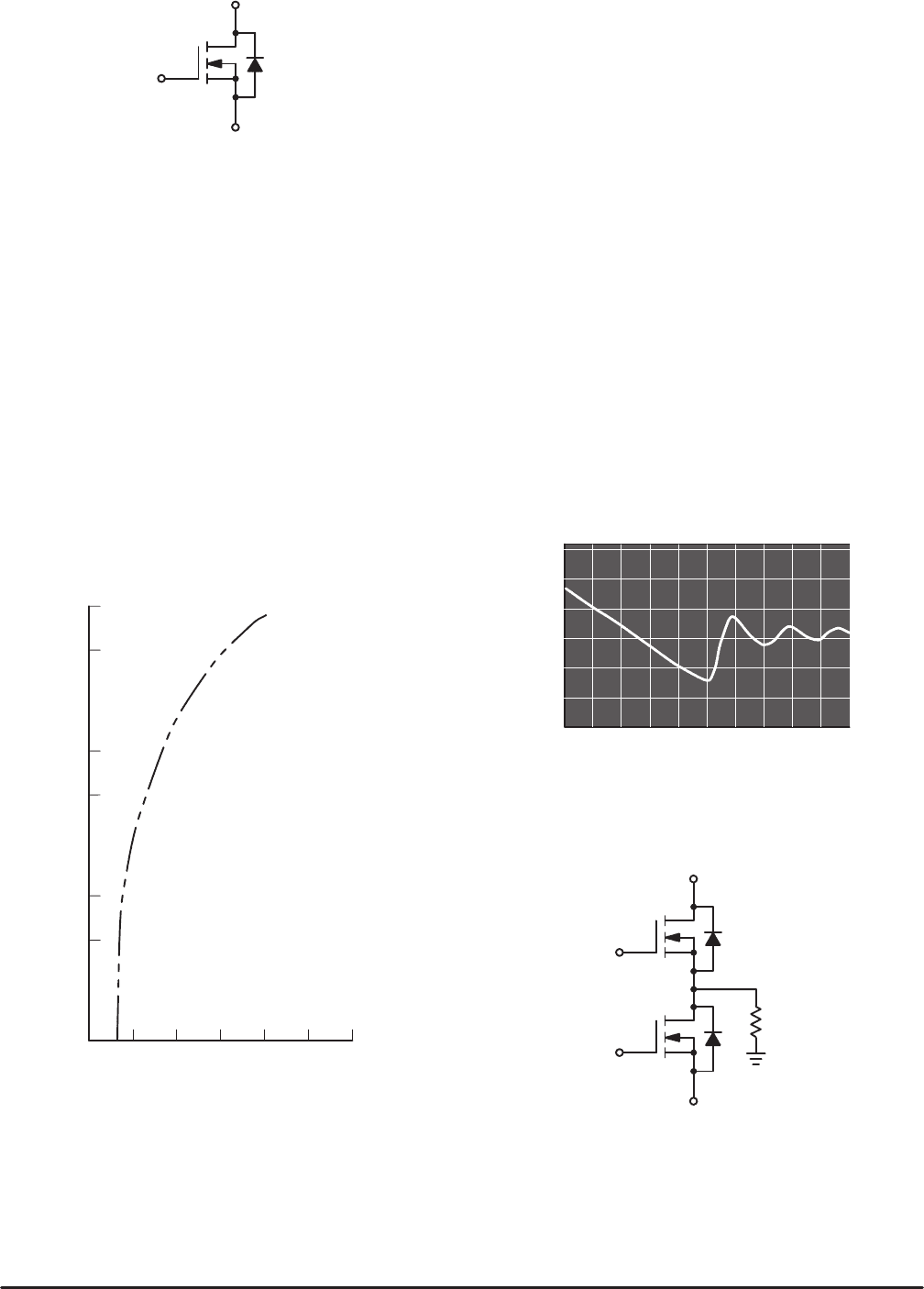
Drain–Source Diode
Inherent in most power MOSFETs, and all TMOS transis-
tors, is a “parasitic” drain–source diode. Figure 2–9, the
illustration of cross section of the TMOS die, shows the P–N
junction formed by the P–well and the N–Epi layer. Because
of its extensive junction area, the current ratings of the diode
are the same as the MOSFET’s continuous and pulsed cur-
rent ratings. For the N–Channel TMOS FET shown in Figure
2–10, this diode is forward biased when the source is at a
positive potential with respect to the drain. Since the diode
may be an important circuit element, Motorola Designer’s
Data Sheets specify typical values of the forward on–voltage,
forward turn–on and reverse recovery time. The forward
characteristic of the drain–source diode of a TMOS power
MOSFET is shown in Figure 2–11.
Figure 2–9. Cross Section of TMOS Cell
SOURCE SITE
N–CHANNEL
DRAIN CURRENT
INSULATING OXIDE, SiO
2
N–SUBSTRATE
N–Epi LAYER
DRAIN
METALIZATION
SOURCE
METALIZATION
SILICON
GATE
Introduction and Basic Characteristics
3–16
Motorola TMOS Power MOSFET Transistor Device Data
Figure 2–10. N–Channel Power MOSFET Symbol
Including Drain–Source Diode
DRAIN
GATE
SOURCE
Most rectifiers, a notable exception being the Schottky
diode, exhibit a “reverse recovery” characteristic as depicted
in Figure 2–12. When forward current flows in a standard
diode, a carrier gradient is formed in the high resistivity side
of the junction resulting in an apparent storage of charge.
Upon sudden application of a reverse bias, the stored charge
temporarily produces a negative current flow during the re-
verse recovery time, or t
rr
, until the charge is depleted. The
circuit conditions that influence t
rr
and the stored charge are
the forward current magnitude and the rate of change of cur-
rent from the forward current magnitude to the reverse cur-
rent peak. When tested under the same circuit conditions,
the parasitic drain–source diode of a TMOS transistor has a
t
rr
similar to that of a fast recovery rectifier.
Figure 2–11. Forward Characteristics of Power
MOSFETs D–S Diodes
100
0.1
1.0 2.0 3.0 6.0
50
10
5.0
1.0
0.5
0 4.0 5.0
I
s
, D–S DIODE FORWARD CURRENT (AMPS)
V
SD
, D–D DIODE FORWARD ON–VOLTAGE (VOLTS)
TC + 25°C
300 µS Pulse 60 pps
In many applications, the drain–source diode is never
forward biased and does not influence circuit operation.
However, in multi–transistor configurations, such as the
totem pole network of Figure 2–13, the parasitic diodes play
an important and useful role. Each transistor is protected
from excessive flyback voltages, not by its own drain–source
diode, but by the diode of the opposite transistor. As an
illustration, assume that Q2 of Figure 2–13 is turned on, Q1
is off and current is flowing up from ground, through the load
and into Q2. When Q2 turns off, current is diverted into the
drain–source diode of Q1 which clamps the load’s inductive
kick to V
+
. By similar reasoning, one can see that D2 protects
Q1 during its turn–off.
As a note of caution, it should be realized that diode recov-
ery problems may arise when using MOSFETs in multiple
transistor configurations. A treatment of the subject in Chap-
ter 5 gives greater details.
TMOS power MOSFET intrinsic diodes also have forward
recovery times, meaning that they do not instantaneously
conduct when they are forward biased. However, since those
times are so brief, typically less than 10 ns, their effect on cir-
cuit operation can almost always be ignored. Package, lead
and wiring inductance are often at least as great a factor in
limiting current rise time.
Figure 2–12. Typical Reverse Recovery
Characteristics of a Drain–Source Diode
0
I
s
= 0.5 A/div
t = 50 ns/div
+V
Q1
Q2
R
L
–V
Figure 2–13. TMOS Totem Pole Network with
Integral Drain–Source Diodes

3–17
Introduction and Basic CharacteristicsMotorola TMOS Power MOSFET Transistors Device Data
Chapter 3: The Data Sheet
Introduction
Motorola prides itself in having one of the most complete
and accurate Power MOSFET data sheets in the industry.
For consistency, data sheet templates have been estab-
lished for each technology and or application grouping. This
insures that the best approach is used in describing the per-
formance characteristics of each device for the applications
they are used in. Additionally, this allows for the automation
of the data sheet generation process which has lead to a
reduction in new product introduction cycle time as well as
providing more accurate and repeatable data.
Headline Information
Motorola’s TMOS Power MOSFET numbering system
contains coded information describing technology, package,
current and voltage information. A complete explanation of
the nomenclature used is contained in Figure 3–1.
MTP75N06HD
MOTOROLA
X FOR ENGINEERING SAMPLES
TMOS
T FOR TMOS
L FOR SMARTDISCRETES
G FOR IGBT
P FOR MULTIPLE CHIP PRODUCTS
PACKAGE TYPE
P FOR PLASTIC TO–220
M FOR METAL TO–204 (TO–3)/ICePAK
D FOR DPAK
A FOR TO–220 ISOLATED
W FOR TO–247
B FOR D
2
PAK
Y FOR TO–264
E FOR SOT–227B
OPTIONAL SUFFIX:
L FOR LOGIC LEVEL
E FOR ENERGY RATED
T4 FOR TAPE & REEL (DPAK/D
2
PAK)
RL FOR TAPE & REEL (DPAK)
HD FOR HIGH CELL DENSITY
V FOR TMOS V (FIVE)
VOLTAGE RATING DIVIDED BY 10
CHANNEL POLARITY, N OR P
Example of exceptions: MTD/MTP3055E
Example of exceptions: MTD/MTP2955E
MMSF4P01HDR1
MOTOROLA
TMOS
M FOR MINIATURE
PACKAGE TYPE
DF — DUAL FET
SF — SINGLE FET
FT — FET TRANSISTOR
CURRENT
OPTIONAL SUFFIX:
E FOR ENERGY RATED
HD FOR HIGH CELL DENSITY
L FOR LOGIC LEVEL
VOLTAGE RATING DIVIDED BY 10
CHANNEL POLARITY, N OR P
C FOR COMPLEMENTARY
SO–8 (MiniMOS) and SOT–223 Power MOSFETs
R1 AND R2 FOR TAPE & REEL
MiniMOS
CURRENT
Figure 3–1. TMOS Power MOSFET Numbering System
