Справочник по мощным TMOS транзисторам (MOTOROLA)
Подождите немного. Документ загружается.


Selector Guide
2–8
Motorola TMOS Power MOSFET Transistor Device Data
TO–220AB (continued)
V
(BR)DSS
(Volts)
Min
@
R
DS(on)
(Ohms)
Max
I
D
(Amps)
Device
I
D
(cont)
Amps
P
D
(1)
(Watts)
Max
Table 13. TO–220AB — P–Channel
500 6 1
MTP2P50E
2 75
200 1 3
MTP6P20E
6
100 0.30 6
MTP12P10
12 88
60 0.45 2.5
MTP5P06V
5 40
0.30 6
MTP2955V
12 60
0.12 11.5
MTP23P06V
23 125
0.08 15
MTP30P06V
30 125
30 0.025 25
MTP50P03HDL
(2)
50 150
(1)
T
C
= 25°C
(2)
Indicates logic level
TO–247 (Isolated Mounting Hole)
V
(BR)DSS
(Volts)
Min
I
D
(Amps)@
R
DS(on)
(Ohms)
Max
Device
I
D
(cont)
Amps
P
D
(1)
(Watts)
Max
Table 14. TO–247 — N–Channel
1000 1.50 3
MTW6N100E
6 180
1.30 5
MTW10N100E
10 250
800 1 3.5
MTW7N80E
7 180
600 0.55 4
MTW8N60E
8 180
500 0.40 7
MTW14N50E
14 180
0.24 10
MTW20N50E
20 250
400 0.24 8
MTW16N40E
16 180
0.16 12
MTW24N40E
24 250
250 0.08 16
MTW32N25E
32 250
200 0.075 16
MTW32N20E
32 180
150 0.05 17.5
MTW35N15E
35 180
100 0.035 22.5
MTW45N10E
45 180
(1)
T
C
= 25°C
TO–264
V
(BR)DSS
(Volts)
Min
@
R
DS(on)
(Ohms)
Max
I
D
(Amps)
Device
I
D
(cont)
Amps
P
D
(1)
(Watts)
Max
Table 15. TO–264 — N–Channel
1000 0.80 7
MTY14N100E
14
568
800 0.50 8
MTY16N80E
16 568
600 0.21 12.5
MTY25N60E
25 568
500 0.26 10
MTY20N50E
20 300
0.15 15
MTY30N50E
30 568
200 0.028 27.5
MTY55N20E
55 568
100 0.011 50
MTY100N10E
100 568
(1)
T
C
= 25°C
Devices listed in
bold, italic
are Motorola preferred devices.

2–9
Selector GuideMotorola TMOS Power MOSFET Transistors Device Data
SOT–227B (ISOTOP)
V
(BR)DSS
(Volts)
Min
@
R
DS(on)
(Ohms)
Max
I
D
(Amps)
Device
I
D
(cont)
Amps
P
D
(1)
(Watts)
Max
Table 16. SOT–227B (ISOTOP)
500 0.15 15
MTE30N50E
30 250
0.08 26.5
MTE53N50E
53 460
200 0.015 62.5
MTE125N20E
125 460
100 0.0055 107
MTE215N10E
215 460
(1)
T
C
= 25°C
SMARTDISCRETES
Table 17. Ignition IGBTs
BV
CES
(Volts)
Clamped
V
CE(on)
@ 10 A
Device
P
D
(1)
(Watts) Max
Package
140 V 1.8
MGP20N14CL
150 TO–220AB
350 V 1.8
MGP20N35CL
150 TO–220AB
MGB20N35CL
2.5
(3)(4)
D
2
PAK
400 V 1.8
MGP20N40CL
150 TO–220AB
MGB20N40CL
2.5
(3)(4)
D
2
PAK
Table 18. TO–220AB
V
(BR)DSS
(Volts) Min
R
DS(on)
(Ohms) Max
I
D
(Amps)
Device
I
D
(cont)
Amps
P
D
(1)
(Watts) Max
60 Clamped Voltage 0.75 1
MLP1N06CL
Current Limited 40
62 Clamped Voltage 0.4 2 MLP2N06CL Current Limited 40
Table 19. DPAK
V
(BR)DSS
(Volts) Min
R
DS(on)
(Ohms) Max
I
D
(Amps)
Device
I
D
(cont)
Amps
P
D
(1)
(Watts) Max
60 Clamped Voltage 0.75 1
MLD1N06CL
Current Limited 1.75
62 Clamped Voltage 0.4 2
MLD2N06CL
Current Limited 1.75
(1)
T
C
= 25°C
(3)
Power rating when mounted on an FR–4 glass epoxy printed circuit board with the minimum recommended footprint.
(4)
Available in tape and reel — add T4 suffix to part number.
Devices listed in
bold, italic
are Motorola preferred devices.
Indicates UL Recognition — File #E69369

Selector Guide
2–10
Motorola TMOS Power MOSFET Transistor Device Data
IGBT — Insulated Gate Bipolar Transistor
Device
BVCES
(V)
IC90
(A)
IC
@ 25°C
(A)
V
CE(on)
@ IC90
(V)
typ
E
off
@ IC90
(mJ)
typ @ 125°C
Package
Table 20. IGBT — N–Channel
MGP20N60
600 20 32 2.90 1.20 TO–220
MGW20N60D
TO–247
MGW30N60
30 50 2.60 1.80 TO–247
MGY30N60D
TO–264
MGY40N60
40 66 2.60 2.40 TO–264
MGY40N60D
MGW10N120
1200 12 20 3.10 1.43 TO–247
MGW10N120D
MGY25N120
25 38 2.90 4.29 TO–264
MGY25N120D
IC90 = Collector current rating at 90°C case temperature
Power MOS Gate Drivers
Device Description Package
Table 21.
MC33153D
V
CC
–V
EE
= 23 V, 1 A Source, 2 A Sink Low Side Driver
8 Pin SOIC
MC33153P
(Can be used as High Side Driver with Opto–coupler)
8 Pin PDIP
MPIC2111D
600 V, 420 mA, Half Bridge Driver
8 Pin SOIC
MPIC2111P 8 Pin PDIP
MPIC2112DW
600 V, 420 mA, Half Bridge Driver
16 Pin SOIC–Wide
MPIC2112P 14 Pin PDIP
MPIC2113DW
600 V, 2 A, Half Bridge Driver
16 Pin SOIC–Wide
MPIC2113P 14 Pin PDIP
MPIC2117D
600 V, 420 mA, High Side Driver
8 Pin SOIC
MPIC2117P 8 Pin PDIP
MPIC2130P
600 V, 420 mA, Three Phase Driver
28 Pin PDIP
MPIC2130FN 44 Pin PLCC (modified)
MPIC2131P
600 V, 420 mA, Three Phase Driver
28 Pin PDIP
MPIC2131FN 44 Pin PLCC (modified)
MPIC2151D
600 V, 210 mA, Self Oscillating, Half Bridge Driver
8 Pin SOIC
MPIC2151P 8 Pin PDIP
Devices listed in
bold, italic
are Motorola preferred devices.

3–1
Introduction and Basic CharacteristicsMotorola TMOS Power MOSFET Transistors Device Data
Section Three
Introduction to Power MOSFETs
Basic Characteristics of Power MOSFETs
Table of Contents
Chapter 1: Introduction to Power MOSFETs
Symbols, Terms and Definitions 3–2. . . . . . . . . . . . . . . . . .
Basic TMOS Structure, Operation and Physics 3–7. . . . .
Distinct Advantages of Power MOSFETs 3–10. . . . . . . . .
Chapter 2: Basic Characteristics of Power MOSFETs
Output Characteristics 3–13. . . . . . . . . . . . . . . . . . . . . . . . .
Basic MOSFET Parameters 3–13. . . . . . . . . . . . . . . . . . . . .
Temperature Dependent Characteristics 3–14. . . . . . . . . .
Drain-Source Diode 3–15. . . . . . . . . . . . . . . . . . . . . . . . . . . .
Chapter 3: The Data Sheet 3–17. . . . . . . . . . . . . . . . . . . . . .

Introduction and Basic Characteristics
3–2
Motorola TMOS Power MOSFET Transistor Device Data
Chapter 1: Introduction to Power MOSFETs
Symbols, Terms and Definitions
The following are the most commonly used letter symbols, terms and definitions associated with Power MOSFETs.
Symbol Term Definition
C
ds
drain–source capacitance The capacitance between the drain and source terminals
with the gate terminal connected to the guard terminal of
a three–terminal bridge.
C
dg
drain–gate capacitance The same as C
rss
– See C
rss
.
C
gs
gate–source capacitance The capacitance between the gate and source terminals
with the drain terminal connected to the guard terminal of
a three–terminal bridge.
C
iss
short–circuit input capacitance,
common–source
The capacitance between the input terminals (gate and
source) with the drain short–circuited to the source for
alternating current. (Ref. IEEE No. 255)
C
oss
short–circuit output capacitance,
common–source
The capacitance between the output terminals (drain and
source) with the gate short–circuited to the source for
alternating current. (Ref. IEEE No. 255)
C
rss
short–circuit reverse transfer
capacitance, common–source
The capacitance between the drain and gate terminals
with the source connected to the guard terminal of a
three–terminal bridge.
g
FS
common–source large–signal
transconductance
The ratio of the change in drain current due to a change in
gate–to–source voltage.
I
D
drain current, dc The direct current into the drain terminal.
I
D(on)
on–state drain current The direct current into the drain terminal with a specified
forward gate–source voltage applied to bias the device to
the on–state.
I
DSS
zero–gate–voltage drain current The direct current into the drain terminal when the
gate–source voltage is zero. This is an on–state current in
a depletion–type device, an off–state in an enhancement–
type device.
I
G
gate current, dc The direct current into the gate terminal.
I
GSS
reverse gate current, drain short–circuited
to source
The direct current into the gate terminal of a junction–gate
field–effect transistor when the gate terminal is reverse
biased with respect to the source terminal and the drain
terminal is short–circuited to the source terminal.
I
GSSF
forward gate current, drain short–circuited
to source
The direct current into the gate terminal of an insulated–
gate field–effect transistor with a forward gate–source
voltage applied and the drain terminal short–circuited to
the source terminal.
I
GSSR
reverse gate current, drain short–circuited
to source
The direct current into the gate terminal of an insulated–
gate field–effect transistor with a reverse gate–source
voltage applied and the drain terminal short–circuited to
the source terminal.

3–3
Introduction and Basic CharacteristicsMotorola TMOS Power MOSFET Transistors Device Data
Symbol Term Definition
I
S
source current, dc The direct current into the source terminal.
P
T
, P
D
total nonreactive power input to all
terminals
The sum of the products of the dc input currents and
voltages.
Q
g
total gate charge The total gate charge required to charge the MOSFETs
input capacitance to V
GS(on)
.
R
DS(on)
static drain–source on–state resistance The dc resistance between the drain and source terminals
with a specified gate–source voltage applied to bias the
device to the on state.
R
θCA
thermal resistance, case–to–ambient The thermal resistance (steady–state) from the device
case to the ambient.
R
θJA
thermal resistance, junction–to–ambient The thermal resistance (steady–state) from the semicon-
ductor junction(s) to the ambient.
R
θJC
thermal resistance, junction–to–case The thermal resistance (steady–state) from the semicon-
ductor junction(s) to a stated location on the case.
R
θJM
thermal resistance, junction–to–mounting
surface
The thermal resistance (steady–state) from the semicon-
ductor junction(s) to a stated location on the mounting
surface.
T
A
ambient temperature or free–air
temperature
The air temperature measured below a device, in an
environment of substantially uniform temperature, cooled
only by natural air convection and not materially affected
by reflective and radiant surfaces.
T
C
case temperature The temperature measured at a specified location on the
case of a device.
t
c
turn–off crossover time The time interval during which drain voltage rises from
10% of its peak off–state value and drain current falls to
10% of its peak on–state value, in both cases ignoring
spikes that are not charge–carrier induced.
T
J
channel temperature The temperature of the channel of a field–effect transistor.
T
stg
storage temperature The temperature at which the device, without any power
applied, may be stored.
t
d(off)
turn–off delay time Synonym for current turn–off delay time (see Note 1)*.
t
d(off)i
current turn–off delay time The interval during which an input pulse that is switching
the transistor from a conducting to a nonconducting state
falls from 90% of its peak amplitude and the drain current
waveform falls to 90% of its on–state amplitude, ignoring
spikes that are not charge–carrier induced.
t
d(off)v
voltage turn–off delay time The time interval during which an input pulse that is
switching the transistor from a conducting to a noncon-
ducting state falls from 90% of its peak amplitude and the
drain voltage waveform rises to 10% of its off–state
amplitude, ignoring spikes that are not charge–carrier
induced.
t
d(on)
turn–on delay time Synonym for current turn–on delay time (see Note 1)*.
t
d(on)i
current turn–on delay time The time interval during which can input pulse that is
switching the transistor from a nonconducting to a
conducting state rises from 10% of its peak amplitude and
the drain current waveform rises to 10% of its on–state
amplitude, ignoring spikes that are not charge–carrier
induced.

Introduction and Basic Characteristics
3–4
Motorola TMOS Power MOSFET Transistor Device Data
Symbol Term Definition
t
d(on)v
voltage turn–on delay time The time interval during which an input pulse that is
switching the transistor from a nonconducting to a
conducting state rises from 10% of its peak amplitude and
the drain voltage waveform falls to 90% of its off–state
amplitude, ignoring spikes that are not charge–carrier
induced.
t
f
fall time Synonym for current fall time (see Note 1)*.
t
fi
current fall time The time interval during which the drain current changes
from 90% to 10% of its peak off–state value, ignoring
spikes that are not charge–carrier induced.
t
fv
voltage fall time The time interval during which the drain voltage changes
from 90% to 10% of its peak off–state value, ignoring
spikes that are not charge–carrier induced.
t
off
turn–off time Synonym for current turn–off time (see Note 1)*.
t
off(i)
current turn–off time The sum of current turn–off delay time and current fall time,
i.e., t
d(off)i
+ t
fi
.
t
off(v)
voltage turn–off time The sum of voltage turn–off delay time and voltage rise
time, i.e., t
d(off)v
+ t
rv
.
t
on
turn–on time Synonym for current turn–on time (see Note 1)*.
t
on(i)
current turn–on time The sum of current turn–on delay time and current rise
time, i.e., t
d(on)i
+ t
ri
.
t
on(v)
voltage turn–on time The sum of voltage turn–on delay time and voltage fall
time, i.e., t
d(on)v
+ t
fv
.
t
p
pulse duration The time interval between a reference point on the leading
edge of a pulse waveform and a reference point on the
trailing edge of the same waveform.
Note: The two reference points are usually 90% of the
steady–state amplitude of the waveform existing after the leading
edge, measured with respect to the steady–state amplitude
existing before the leading edge. If the reference points are 50%
points, the symbol t
w
and term average pulse duration should be
used.
t
r
rise time Synonym for current rise time (see Note 1)*.
t
ri
current rise time The time interval during which the drain current changes
from 10% to 90% of its peak on–state value, ignoring
spikes that are not charge–carrier induced.
t
rv
voltage rise time The time interval during which the drain voltage changes
from 10% to 90% of its peak off–state value, ignoring
spikes that are not charge–carrier induced.
t
ti
current fall time The time interval following current fall time during which
the drain current changes from 10% to 2% of its peak
on–state value, ignoring spikes that are not charge–carrier
induced.
t
w
average pulse duration The time interval between a reference point on the leading
edge of a pulse waveform and a reference point on the
trailing edge of the same waveform, with both reference
points being 50% of the steady–state amplitude of the
waveform existing after the leading edge, measured with
respect to the steady–state amplitude existing before the
leading edge.
Note: If the reference points are not 50% points, the symbol t
p
and term pulse duration should be used.

3–5
Introduction and Basic CharacteristicsMotorola TMOS Power MOSFET Transistors Device Data
Symbol Term Definition
V
(BR)DSR
drain–source breakdown voltage with
(resistance between gate and source)
The breakdown voltage between the drain terminal and the
source terminal when the gate terminal is (as indicated by
the last subscript letter) as follows:
R = returned to the source terminal through a specified
resistance.
V
(BR)DSS
gate short–circuited to source S = short–circuited to the source terminal.
V
(BR)DSV
voltage between gate and source V = returned to the source terminal through a specified
voltage.
V
(BR)DSX
circuit between gate and source X = returned to the source terminal through a specified
circuit.
V
(BR)GSSF
forward gate–source breakdown voltage The breakdown voltage between the gate and source
terminals with a forward gate–source voltage applied and
the drain terminal short–circuited to the source terminal.
V
(BR)GSSR
reverse gate–source breakdown voltage The breakdown voltage between the gate and source
terminals with a reverse gate–source voltage applied and
the drain terminal short–circuited to the source terminal.
V
DD
, V
GG
V
SS
supply voltage, dc (drain, gate, source)
voltage
The dc supply voltage applied to a circuit or connected to
the reference terminal.
V
DG
V
DS
V
GD
V
GS
V
SD
V
SG
drain–to–gate
drain–to–source
gate–to–drain
gate–to–source
source–to–drain
source–to–gate
The dc voltage between the terminal indicated by the first
subscript and the reference terminal indicated by the
second subscript (stated in terms of the polarity at the
terminal indicated by the first subscript).
V
DS(on)
drain–source on–state voltage The voltage between the drain and source terminals with
a specified forward gate–source voltage applied to bias the
device to the on state.
V
GS(th)
gate–source threshold voltage The forward gate–source voltage at which the magnitude
of the drain current of an enhancement–type field–effect
transistor has been increased to a specified low value.
Z
θJA(t)
transient thermal impedance,
junction–to–ambient
The transient thermal impedance from the semiconductor
junction(s) to the ambient.
Z
θJC(t)
transient thermal impedance,
junction–to–case
The transient thermal impedance from the semiconductor
junction(s) to a stated location on the case.
Note 1: As names of time intervals for characterizing switching transistors, the terms “fall time” and “rise time” always refer to the change that is
taking place in the magnitude of the output current even though measurements may be made using voltage waveforms. In a purely resistive
circuit, the (current) rise time may be considered equal and coincident to the voltage fall time and the (current) fall time may be considered equal
and coincident to the voltage rise time. The delay times for current and voltage will be equal and coincident. When significant amounts of
inductance are present in a circuit, these equalities and coincidences no longer exist, and use of the unmodified terms delay time, fall time, and
rise time must be avoided.

Introduction and Basic Characteristics
3–6
Motorola TMOS Power MOSFET Transistor Device Data
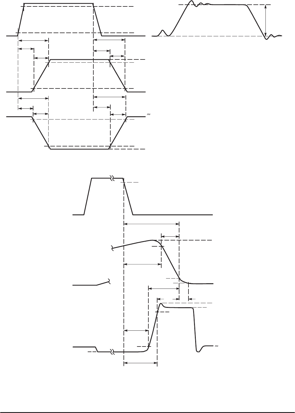
Figure 1–1. Waveforms for Resistive–Load Switching
Figure 1–2. Waveforms for Inductive Load Switching, Turn–Off
NOTE: V
clamp
(in a clamped inductive–load switching circuit) or V
(BR)DSX
(in an unclamped circuit) is the peak off–state voltage
excluding spikes.
90%
Input Voltage
(Idealized wave shape)
10%
90%
10%
90%
10%
Drain
Voltage
(Idealized wave shape)
Drain
Current
(Idealized wave shape)
Drain
Current
(Practical wave shape
including spikes caused
by currents that are
not charge–carrier
induced)
t
off
≅ t
off(i)
t
off
≅ t
on(i)
t
d(off)
= t
d(off)i
I
D(on)
t
f
≅ t
fi
t
d(off)v
I
D(off)
t
off(v)
t
rv
t
fv
t
r
≅ t
ri
td
(on)
= td
(on)i
t
on(v)
t
d(on)v
V
DS(on)
100%
Pulse
amplitude
V
DD
90%
Input
Voltage
2%
10%
Drain
Voltage
Drain
Current
t
off(i)
t
d(off)i
I
DM
t
fi
t
d(off)v
I
D(off)
t
off(v)
t
ti
t
rv
V
DSM
V
DD
90%
10%
90%
t
c
(or t
xo
)
V
clamp
or V
(BR)DSX
(See Note)
V
DS(on)

3–7
Introduction and Basic CharacteristicsMotorola TMOS Power MOSFET Transistors Device Data
Basic TMOS Structure, Operation and Physics
Structures:
Motorola’s TMOS Power MOSFET family is a matrix of dif-
fused channel, vertical, metal–oxide–semiconductor power
field–effect transistors which offer an exceptionally wide
range of voltages and currents with low R
DS(on)
. The inherent
advantages of Motorola’s power MOSFETs include:
• Nearly infinite static input impedance featuring:
— Voltage driven input
— Low input power
— Few driver circuit components
• Very fast switching times
— No minority carriers
— Minimal turn–off delay time
— Large reversed biased safe operating area
— High gain bandwidth product
• Positive temperature coefficient of on–resistance
— Large forward biased safe operating area
— Ease in paralleling
• Almost constant transconductance
• High dv/dt immunity
Motorola’s TMOS power MOSFET line is the latest step in
an evolutionary progression that began with the conventional
small–signal MOSFET and superseded the intermediate lat-
eral double diffused MOSFET (LDMOSFET) and the vertical
V–groove MOSFET (VMOSFET).
The conventional small–signal lateral N–channel
MOSFET consists of a lightly doped P–type substrate into
which two highly doped N
+
regions are diffused, as shown in
Figure 1–3. The N
+
regions act as source and drain which
are separated by a channel whose length is determined by
photolithographic constraints. This configuration resulted in
long channel lengths, low current capability, low reverse
blocking voltage and high R
DS(on)
.
Two major changes in the small–signal MOSFET structure
were responsible for the evolution of the power MOSFET.
One was the use of self aligned, double diffusion techniques
to achieve very short channel lengths, which allowed higher
channel packing densities, resulting in higher current capa-
bility and lower R
DS(on)
. The other was the incorporation of a
lightly doped N
+
region between the channel and the N
+
drain allowing high reverse blocking voltages.
These changes resulted in the lateral double diffused
MOSFET power transistor (LDMOS) structure shown in
Figure 1–4, in which all the device terminals are still on the
top surface of the die. The major disadvantage of this config-
uration is its inefficient use of silicon area due to the area
needed for the top drain contact.
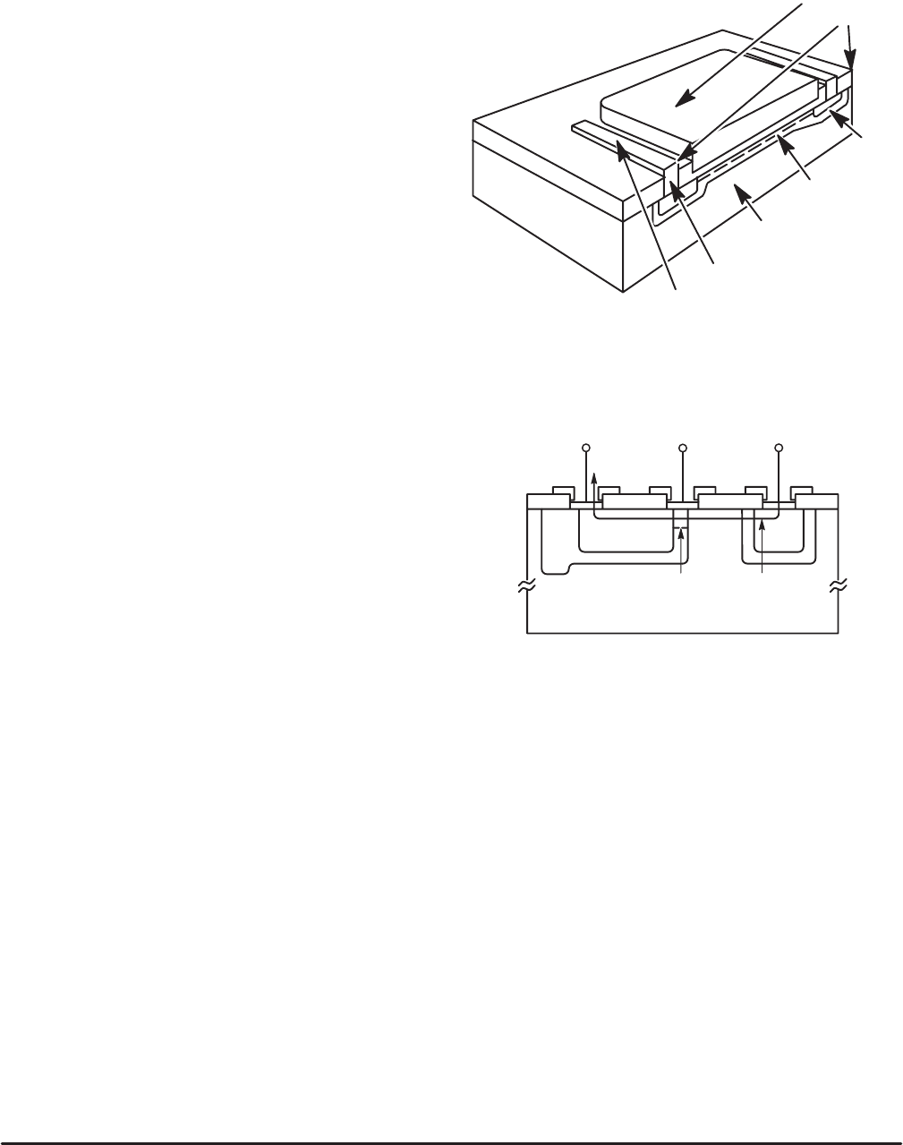
Figure 1–3. Conventional Small–Signal MOSFET has
Long Lateral Channel Resulting in Relatively High
Drain–to–Source Resistance
DRAIN METAL + V
DD
SOURCE METAL
P–SUBSTRATE
AND BODY
N–CHANNEL
(CURRENT PATH)
DEPLETION
REGION
GA
TE + V
G
CURRENT
Figure 1–4. Lateral Double Diffused MOSFET
Structure Featuring Short Channel Lengths and High
Packing Densities for Lower On Resistance
Channel
Current
N –
N + N +
P
SiO
2
DSG
The next step in the evolutionary process was a vertical
structure in which the drain contact was on the back of the
die, further increasing the channel packing density. The initial
concept used a V–groove MOSFET power transistor as
shown in Figure 1–5. The channels in this device are defined
by preferentially etching V–grooves through double diffused
N
+
and P
–
regions. The requirements of adequate packing
density, efficient silicon usage and adequate reverse block-
ing voltage are all met by this configuration. However, due to
its non–planar structure, process consistency and cleanli-
ness requirements resulted in higher die costs.
