Power electronic handbook
Подождите немного. Документ загружается.

186 J. Rodríguez et al.
0
0
v
T1
v
d
i
d
i
s
v
s
+
v
T1
T
1
L
L
d
V
L
(a)
(b)
(c)
0
0
0
v
s
−v
s
i
g1
, i
g2
i
g3
, i
g4
v
d
v
s
−v
s
V
dia
v
d
T
3
T
4
T
2
ωt
ωt
ωt
ωt
ωt
α = 135°
m
g
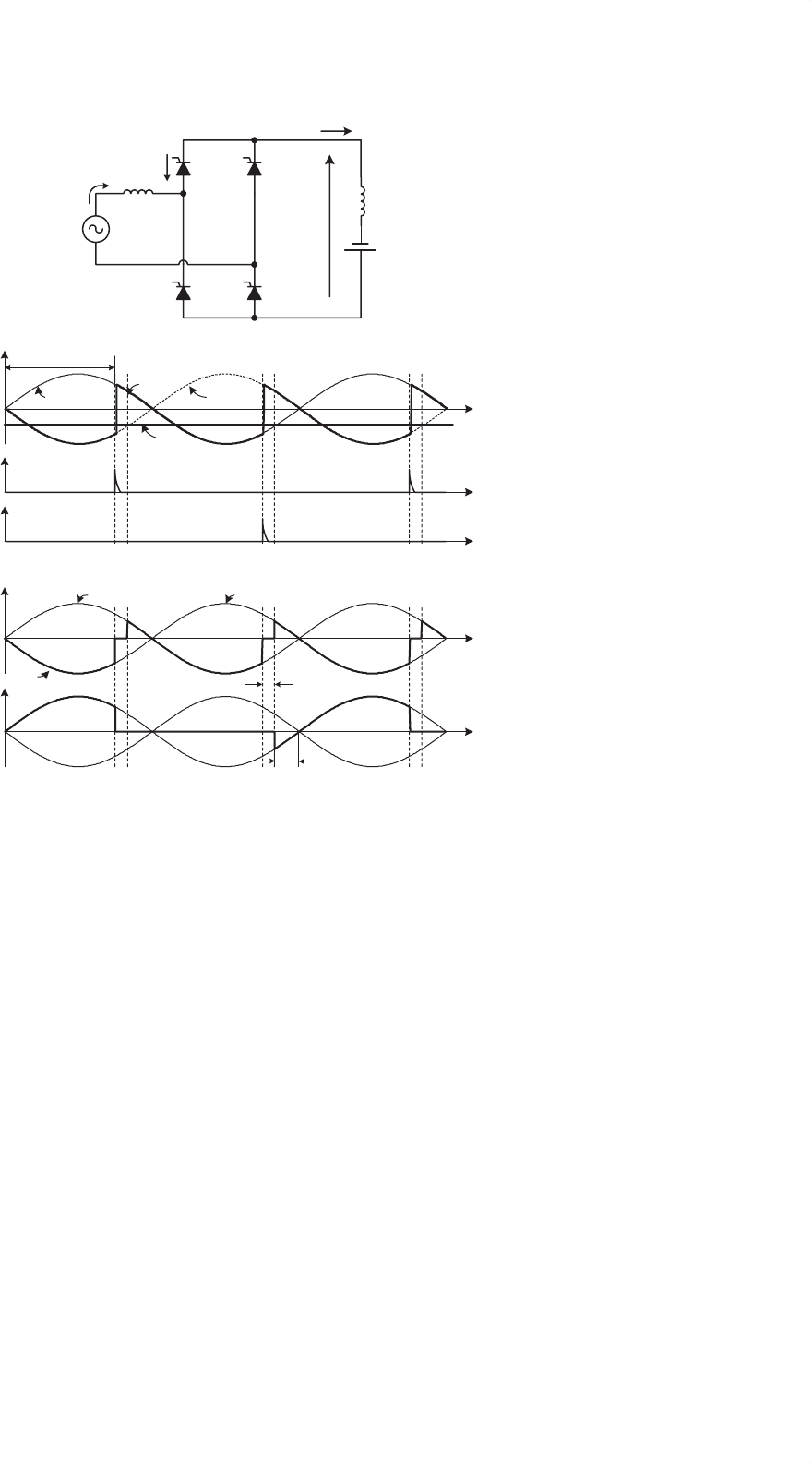
FIGURE 11.11 Rectifier in the inverting mode: (a) circuit; (b) waveforms neglecting source inductance L; and (c) waveforms considering L.
where ω is the supply frequency and t
q
is the thyristor turn-
off time. Considering Eqs. (11.23) and (11.24) the maximum
firing angle is, in practice,
α
max
= 180 −µ −γ (11.25)
If the condition of Eq. (11.25) is not satisfied, the commutation
process will fail, originating destructive currents.
11.2.8 Applications
Important application areas of controlled rectifiers include
uninterruptible power supplies (UPS), for feeding critical
loads. Figure 11.12 shows a simplified diagram of a single-
phase UPS configuration, typically rated for <10 kVA. A fully
controlled or half-controlled rectifier is used to generate the
dc voltage for the inverter. In addition, the input rectifier acts
as a battery charger. The output of the inverter is filtered before
it is fed to the load. The most important operation modes of
the UPS are:
(i) Normal mode. In this case the line voltage is present.
The critical load is fed through the rectifier-inverter
scheme. The rectifier keeps the battery charged.
(ii) Outage mode. During a loss of the ac main supply,
the battery provides the energy for the inverter.
(iii) Bypass operation. When the load demands an over-
current to the inverter, the static bypass switch is
turned on and the critical load is fed directly from
the mains.
The control of low power dc motors is another interesting
application of controlled single-phase rectifiers. In the circuit
of Fig. 11.13, the controlled rectifier regulates the armature
voltage and consequently controls the motor current i
d
in
order to produce a required torque.
This configuration allows only positive current flow in
the load. However the load voltage can be both positive
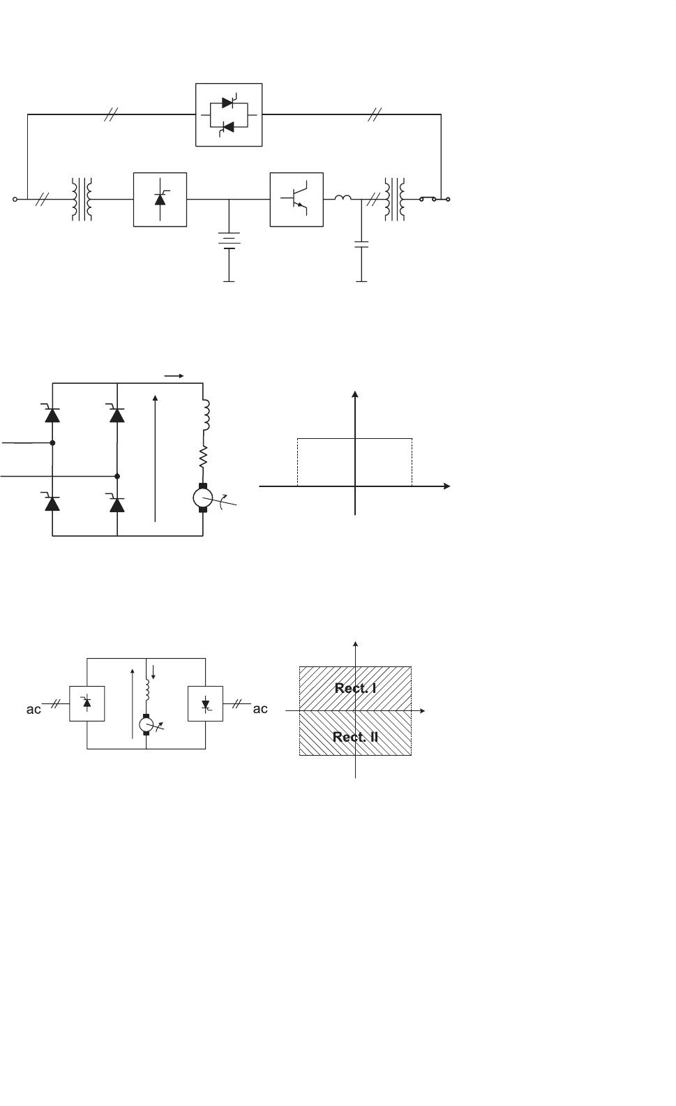
11 Single-phase Controlled Rectifiers 187
LoadGrid
InverterRectifier
Filter
Battery
Bypass switch
FIGURE 11.12 Application of a rectifier in single-phase UPS.
w
r
i
d
i
d
V
da
V
d
0
(a) (b)
FIGURE 11.13 Two-quadrant dc drive: (a) circuit and (b) quadrants of operation.
T~i
d
0
w
r
Rect II
v
d
Rect I
i
d
(a) (b)
w
r
FIGURE 11.14 Single-phase dual-converter drive: (a) connection and (b) four-quadrant operation.
and negative. For this reason, this converter works in the
two-quadrant mode of operation in the plane i
d
vs V
dα
.
A better performance can be obtained with two rectifiers
in back-to-back connection at the dc terminals, as shown in
Fig. 11.14a. This arrangement, known as a dual converter
configuration, allows four-quadrant operation of the drive.
Rectifier I provides positive load current i
d
, while rectifier II
provides negative load current. The motor can work in forward
powering, forward braking (regenerating), reverse powering,
and reverse braking (regenerating). These operating modes are
shown in Fig. 11.14b, where the torque T vs the rotor speed ω
r
is illustrated.
188 J. Rodríguez et al.
−15 −400
400
−300
300
−200
200
−100
100
0
−10
−5
0
5
10
15
0,005 0,01
0,015
0,02 0,025 0,03
Time [s]
I [A]
V[V]
Class D Envelope
v
s
v
s
i
s
i
s
+
L
C
(a) (b)
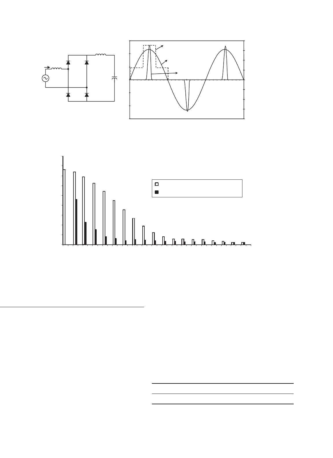
FIGURE 11.15 Single-phase rectifier: (a) circuit and (b) waveforms of the input voltage and current.
0.0
0.5
1.0
1.5
2.0
2.5
3.0
3.5
4.0
4.5
1 5 9 11 13 15 17 19 21 23 25 27 29 31 33 35
Single phase diode bridge rectifier
Standard IEC 61000-3-2 Class D
Harmonic order
Current amplitude [A]
37 37
FIGURE 11.16 Input current harmonics produced by a single-phase diode bridge rectifier.
11.3 Unity Power Factor Single-phase
Rectifiers
11.3.1 The Problem of Power Factor in
Single-phase Line-commutated Rectifiers
The main disadvantages of the classical line-commutated rec-
tifiers are that (i) they produce a lagging displacement factor
with respect to the voltage of the utility; (ii) they generate an
important amount of input current harmonics.
These aspects have a negative influence on both power fac-
tor and power quality. In the last several years, the massive use
of single-phase power converters has increased the problems of
power quality in electrical systems. In effect, modern commer-
cial buildings have 50% and even up to 90% of the demand,
originated by non-linear loads, which are composed mainly by
rectifiers [1]. Today it is not unusual to find rectifiers with total
harmonic distortion of the current THD
i
> 40%, originating
severe overloads in conductors and transformers.
Figure 11.15a shows a single-phase rectifier with a capac-
itive filter, used in much of today’s low-power equipment.
The input current produced by this rectifier is illustrated in
Fig. 11.15b, it appears highly distorted due to the presence of
the filter capacitor. This current has a harmonic content shown
in Fig. 11.16 and Table 11.1, with a THD
i
= 197%.
The rectifier in Fig. 11.15 has a very low power factor of
PF = 0.45, due mainly to its large harmonic content.
TABLE 11.1 Harmonic content of the current of Fig. 11.15
n 3579111315171921
I
n
/I
1
[%] 96.8 90.5 81.7 71.0 59.3 47.3 35.7 25.4 16.8 10.6
11 Single-phase Controlled Rectifiers 189
11.3.2 Standards for Harmonics in Single-phase
Rectifiers
The relevance of the problems originated by harmonics in
single-phase line-commutated rectifiers has motivated some
agencies to introduce restrictions to these converters. The IEC
61000-3-2 Class D International Standard establishes limits to
all low-power single-phase equipment having an input cur-
rent with a “special wave shape” and an active input power
P ≤ 600 W. Class D equipment has an input current with
a special wave shape contained within the envelope given
in Fig. 11.15b. This class of equipment must satisfy certain
harmonic limits, shown in Fig. 11.16. It is clear that a single-
phase line-commutated rectifier with the parameters shown in
Fig. 11.15a is not able to comply with the standard IEC 61000-
3-2 Class D. The standard can be satisfied only by adding huge
passive filters, which increases the size, weight, and cost of the
rectifier. This standard has been the motivation for the devel-
opment of active methods to improve the quality of the input
current and, consequently, the power factor.
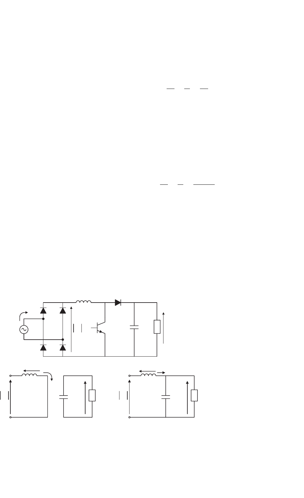
11.3.3 The Single-phase Boost Rectifier
One of the most important high power factor rectifiers, from
a theoretical and conceptual point of view, is the so-called
single-phase boost rectifier, shown in Fig. 11.17a, which is
obtained from a classical non-controlled bridge rectifier, with
the addition of transistor T, diode D, and inductor L.
11.3.3.1 Working Principle, Basic Concepts
In boost rectifiers, the input current i
s
(t) is controlled
by changing the conduction state of transistor T. When
L
x
C
D
L
C
Load
(a)
(b)
+
L
C
Load
(c)
i
L
v
L
v
o
i
s
v
s
v
o
i
L
v
L
v
s
v
s
v
s
v
o
FIGURE 11.17 Single-phase boost rectifier: (a) power circuit and equivalent circuit for transistor T in; (b) on-state; and (c) off-state.
transistor T is in the on-state, the single-phase power sup-
ply is short-circuited through the inductance L, as shown in
Fig. 11.17b; the diode D avoids the discharge of the filter capac-
itor C through the transistor. The current of the inductance i
L
is given by the following equation
di
L
dt
=
v
L
L
=
|
v
s
|
L
(11.26)
Due to the fact that |v
s
| > 0, the on-state of transistor T
always produces an increase in the inductance current i
L
and
consequently an increase in the absolute value of the source
current i
s
.
When transistor T is turned off, the inductor current i
L
cannot be interrupted abruptly and flows through diode D,
charging capacitor C. This is observed in the equivalent circuit
of Fig. 11.17c. In this condition, the behavior of the inductor
current is described by
di
L
dt
=
v
L
L
=
|
v
s
|
−v
o
L
(11.27)
If v
o
> |v
s
|, which is an important condition for the correct
behavior of the rectifier, then |v
s
|−v
o
< 0, and this means that
in the off-state the inductor current decreases its instantaneous
value.
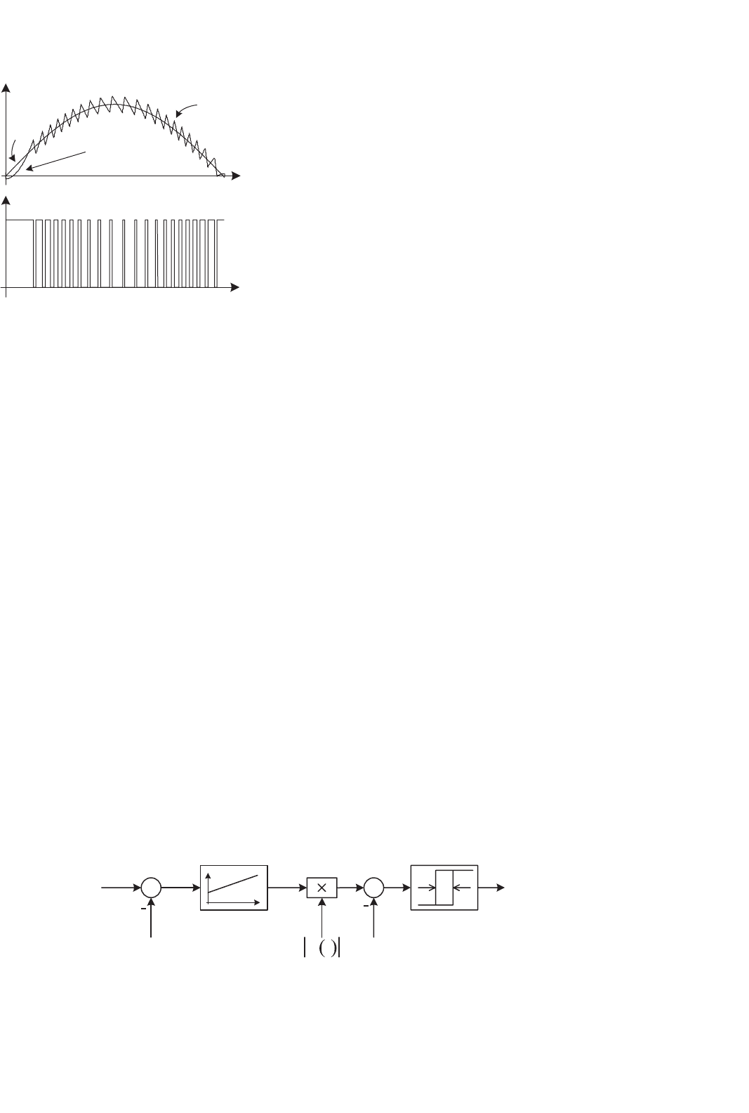
11.3.3.2 Continuous Conduction Mode (CCM)
With an appropriate firing pulse sequence is applied to transis-
tor T, the waveform of the input current i
s
can be controlled to
follow a sinusoidal reference, as can be observed in the positive
half-wave of i
s
in Fig. 11.18. This figure shows the reference
190 J. Rodríguez et al.
Current
distortion
(a)
(b)
i
Lref
i
L
0
0
1
x
FIGURE 11.18 Behavior of the inductor current i
L
: (a) waveforms and
(b) transistor T gate drive signal x.
inductor current i
Lref
, the inductor current i
L
and the gate
drive signal x for transistor T. Transistor T is on when x = 1
and it is off when x = 0.
Figure 11.18 clearly shows that the on- (off-) state of
transistor T produces an increase (decrease) in the inductor
current i
L
.
Note that for low values of v
s
the inductor does not have
enough energy to increase the current value, for this reason it
presents a distortion in their current waveform as shown in
Fig. 11.18a.
Figure 11.19 presents a block diagram of the control system
for the boost rectifier, which includes a proportional-integral
(PI) controller, to regulate the output voltage v
o
. The reference
value i
Lref
for the inner current control loop is obtained from
the multiplication between the output of the voltage controller
and the absolute value |v
s
(t)|. A hysteresis controller provides a
fast control for the inductor current i
L
, resulting in a practically
sinusoidal input current i
s
.
Typically, the output voltage v
o
should be at least 10%
higher than the peak value of the source voltage v
s
(t), in order
to assure good dynamic control of the current. The control
works with the following strategy: a step increase in the refer-
ence voltage v
oref
will produce an increase in the voltage error
v
oref
− v
o
and an increase of the output of the PI controller,
which originates an increase in the amplitude of the reference
v
oref
v
o
PI
v
s
t
+
i
Lref
x
i
L
+
d
FIGURE 11.19 Control system of the boost rectifier.
current i
Lref
. The current controller will follow this new ref-
erence and will increase the amplitude of the sinusoidal input
current i
s
, which will increase the active power delivered by
the single-phase power supply, producing finally an increase
in the output voltage v
o
.
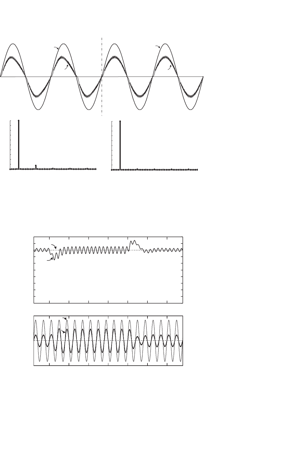
Figure 11.20a shows the waveform of the input current i
s
and the source voltage v
s
. The ripple of the input current can
be reduced by shortening the hysteresis width δ. The tradeoff
for this improvement is an increase in the switching frequency,
which is proportional to the commutation losses of the transis-
tors. For a given hysteresis width δ, a reduction of inductance L
also produces an increase in the switching frequency. As can be
seen, the input current presents a third-harmonic component.
This harmonic is generated by the second-harmonic compo-
nent present in v
o
, which is fed back through the voltage (PI)
controller and multiplied by the sinusoidal waveform, gener-
ating a third-harmonic component on i
Lref
. This harmonic
contamination can be avoided by filtering the v
o
measure-
ment with a lowpass filter or a bandstop filter around 2ω
s
.
The input current obtained using the measurement filter is
shown in Fig. 11.20b. Figure 11.20d confirms the reduction of
the third-harmonic component.
However, in both cases, a drastic reduction in the harmonic
content of the input current i
s
can be observed in the frequency
spectrum of Figs. 11.20c and 11.20d. This current fulfills
the restrictions established by standard IEC 61000-3-2. The
total harmonic distortion of the current in Fig. 11.20a is
THD = 7.46%, while the THD of the current of Fig. 11.20b
is 4.83%, in both cases a very high power factor, over 0.99,
is reached.
Figure 11.21 shows the dc voltage control loop dynamic
behavior for step changes in the load. An increase in the load,
at t = 0.3 [s], produces an initial reduction of the output
voltage v
o
, which is compensated by an increase in the input
current i
s
.Att = 0.6 [s] a step decrease in the load is applied.
The dc voltage controller again adjusts the supply current in
order to balance the active power.
11.3.3.3 Discontinuous Conduction Mode (DCM)
This PFC method is based on an active current waveform-
shaping principle. There are two different approaches consid-
ering fixed and variable switching frequency, both operating
principles are illustrated in Fig. 11.22.
11 Single-phase Controlled Rectifiers 191
Without Filter With Filter
0
20
40
60
80
100
0 250 450
0
20
40
60
80
100
v
s
i
s
v
s
Frequency [Hz] Frequency [Hz]
t
(a) (b)
(c) (d)
% of Fundamental
% of Fundamental
i
s
35015050 0 250 45035015050
FIGURE 11.20 Input current and voltage of the single-phase boost rectifier: (a) without a filter on v
o
measurement; (b) with a filter on v
o
measurement; frequency spectrum; (c) without filter; and (d) with filter.
0.3 0.35 0.4 0.45 0.5 0.55 0.6
0
100
200
300
500
400
350
450
150
250
50
0
Time [s]
20
40
60
-40
-20
-60
Input Current i
s
[A] DC-link Voltage v
o
[V]
i
s
v
s
v
oref
(a)
(b)
v
o
FIGURE 11.21 Response to a change in the load: (a) output-voltage v
o
and (b) input current i
s
.
192 J. Rodríguez et al.
Mode 1 Mode 2 Mode 3
i
L
i
L
, i
D
i
s
t
S
t
on
t
off
T
s
t
(a)
i
L
i
L
, i
D
i
s
t
S
t
on
t
off
T
s
t
~
(b)
Mode 1 Mode 2
FIGURE 11.22 Boost DCM operating principle: (a) with fixed switching frequency and (b) with variable switching frequency.
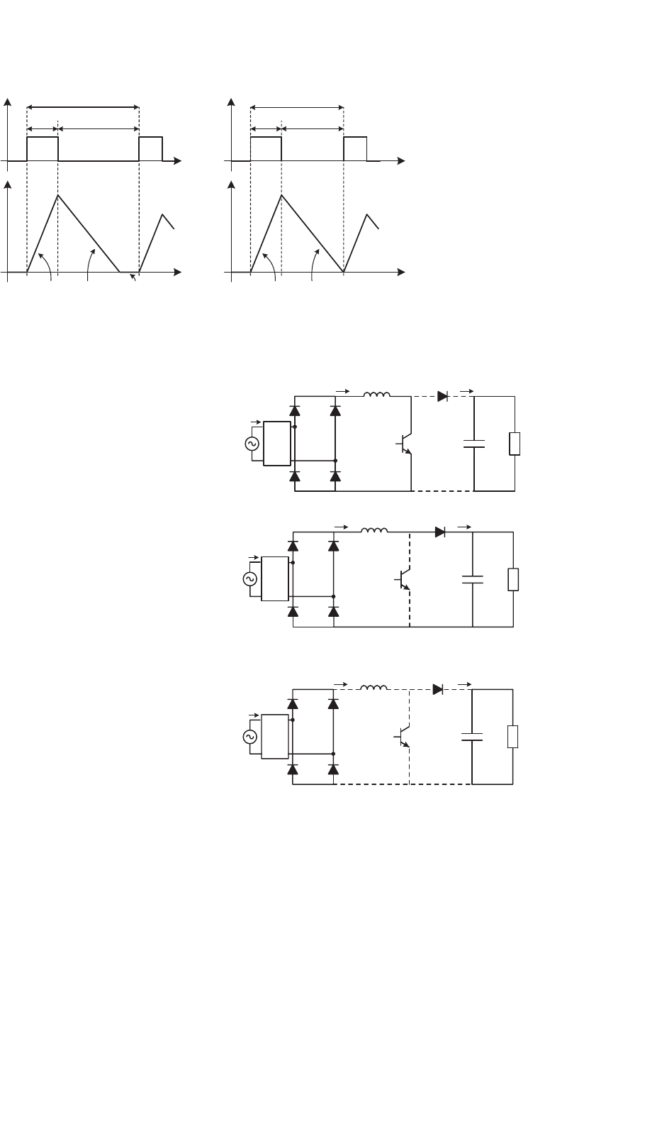
a) DCM with Fixed Switching Frequency
The current shaping strategy is achieved by combining three
different conduction modes, performed over a fixed switch-
ing period T
s
. At the beginning of each period the power
semiconductor is turned on. During the on-state, shown in
Fig. 11.23a, the power supply is short-circuited through the
rectifier diodes, the inductor L, and the boost switch T. Hence,
the inductor current i
L
increases at a rate proportional to the
instantaneous value of the supply voltage. As a result, during
the on-state, the average supply current i
s
is proportional to
the supply voltage v
s
which yields to power factor correction.
When the switch is turned off, the current flows to the load
trough diode D, as shown in Fig. 11.23b. The instantaneous
current value decreases (since the load voltage v
o
is higher than
the supply peak voltage) at a rate proportional to the difference
between the supply and load voltage. Finally, the last mode,
illustrated in Fig. 11.23c, corresponds to the time in which the
current reaches zero value, completing the switching period T
s
.
Therefore, the supply current is not proportional to the voltage
source during the whole control period, introducing distortion
and undesirable EMI in comparison to CCM.
The duty cycle D = t
on
/T
s
is determined by the control
loop, in order to obtain the desired output power and to
ensure operation in DCM, i.e. to reach zero current before
the new switching cycle starts. The control strategy can be
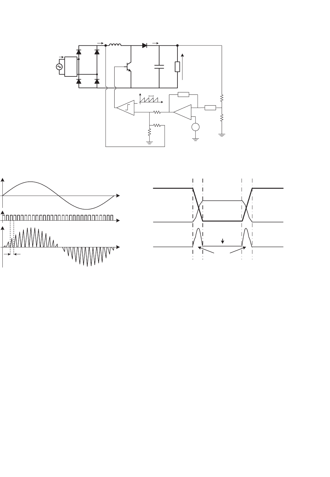
implemented with analog circuitry as shown in Fig. 11.24, or
digitally with modern computing devices. Generally, the duty
cycle is controlled with a slow control loop, maintaining the
output voltage and duty cycle constant over a half-source cycle.
A qualitative example of the supply voltage and current
obtained using DCM is illustrated in Fig. 11.25.
b) DCM with Variable Switching Frequency
The operating principle is similar to the one used in the previ-
ous case, the main difference is that mode 3 is avoided by
switching the transistor again to the on-state, immediately
after the inductor current reaches zero value. This reduces
i
L
D
i
D
=0
L
C
Load
T
v
s
+
i
s
(a)
i
L
D
i
D
L
C
T
+
EMI
Filter
EMI
Filter
EMI
Filter
(b)
Load
v
s
i
s
i
L
=0
D
i
D
=0
L
C
T
+
(c)
Load
v
s
i
s
FIGURE 11.23 Boost DCM equivalent circuits: (a) mode 1: transistor
on, inductor current increasing; (b) mode 2: transistor off, inductor cur-
rent decreasing; and (c) mode 3: transistor off, inductor current reaches
zero.
the current distortion, with the tradeoff of introducing vari-
able switching frequency (T
s
is variable) and consequently
lower-order harmonic content.
Both CCM and DCM achieve an improvement in the power
factor. The DCM is more efficient since reverse-recovery losses
11 Single-phase Controlled Rectifiers 193
i
L
D
i
D
L
C
T
+
_
_
+
+
_
Ramp
T
s
OP
v
o
*
R
1
R
1
R
2
R
3
R
4
Z
1
Z
2
S
v
o
v
s
+
i
s
EMI
Filter
FIGURE 11.24 Boost DCM control circuit with fixed switching frequency.
i
s
t
S
t
t
v
s
T
s
FIGURE 11.25 Boost DCM waveforms: supply voltage, transistor con-
trol signal, and supply current.
of the boost diode are eliminated, however this mode intro-
duces high-current ripple and considerable distortion and
usually an important fifth-order harmonic is obtained. There-
fore boost-DCM applications are limited to 300 W power
levels, to meet standards and regulations. The DCM with vari-
able switching frequency reduces this harmonic content, at
expends of a wide distributed current spectrum and all related
design problems.
11.3.3.4 Resonant Structures for the Boost Rectifiers
An important issue in power electronics is the power losses in
power semiconductors. These losses can be classified in two
groups: conduction losses and switching losses, as shown in
Fig. 11.26.
The conduction losses are produced by the current through
the semiconductor juncture, so these losses are unavoidable.
Switching
losses
Conduction
losses
Current
Voltage CE
OFF OFFON
FIGURE 11.26 Conduction and switching losses on a power switch.
However, the switching losses, which are produced while the
power semiconductors work in linear state during the tran-
sition from on- to off- state or from off- to on-state, can be
reduced or even eliminated, if the switch (transition) occurs
when: (a) the current across the power semiconductor is zero;
(b) the voltage between the power terminals of the power
semiconductor is zero.
This operation mode is used in the so-called resonant or soft-
switched converters, which are discussed in detail in a different
chapter of this handbook.
Resonant operation can also be used with the boost con-
verter topology. In order to produce this condition, topology
of Fig. 11.17 needs to be modified, by including reactive
components and additional semiconductors.
In Fig. 11.27 a resonant structure for zero current switch-
ing (ZCS) [2] is shown. As can be seen, additional resonant
inductors (L
r1
, L
r2
), capacitors (C
r
), diodes (D
r1
,D
r2
), and
power switch (S
r
) have been included.
194 J. Rodríguez et al.
C
L
S
C
r
S
r
L
r1
L
r2
D
r1
D
r2
D
R
Resonant Components
v
s
FIGURE 11.27 Boost rectifier with ZCS.
C
L
S
C
r
S
r
L
r
D
r1
D
r2
R
Resonant
Components
v
s
FIGURE 11.28 Boost rectifier with ZVS.
In a similar way, in Fig. 11.28 a resonant structure for zero
voltage switching (ZVS) [3] is shown. Once again, additional
inductance (L
r
), capacitor (C
r
), and power switch (S
r
) are
added, note however, that diode D has been replaced by two
“resonant diodes,” D
r1
and D
r2
.
In both cases, the ZVS or ZCS condition is reached through
a proper control of S
r
. Other resonant topologies are described
in the literature [4–6] with similar behavior.
v
s
i
s
T
2
T
1
v
o
L
C
R
T
2
v
s
i
s
L
v
s
i
s
T
1
v
o
R
L
C
(a)
(b) (c)
D
2
D
1
D
1
D
2
v
o
R
C
FIGURE 11.29 (a) Power circuit of bridgless boost rectifier; equivalent circuit when; (b) v
s
>0; and (c) v
s
<0.
11.3.3.5 Bridgless Boost Rectifier
The bridgless boost rectifier [7] is shown in Fig. 11.29a. This
rectifier replaces the input diode rectifier by a combination
of two boost rectifiers which work alternately: (a) when v
s
is
positive, T
1
and D
1
operate as boost rectifier 1 (Fig. 11.29b);
(b) when v
s
is negative, T
2
and D
2
operate as boost rectifier 2
(Fig. 11.29c);
This topology reduces the conduction losses of the rectifier
[8, 9], but requires a slightly more complex control scheme,
also EMI and EMC aspects must be considered.
11.3.4 Voltage Doubler PWM Rectifier
Figure 11.30a shows the power circuit of the voltage doubler
pulse width modulated (PWM) rectifier, which uses two tran-
sistors T
1
and T
2
and two filter capacitors C
1
and C
2
. The
transistors are switched complementary to control the wave-
form of the input current i
s
and the output dc voltage v
o
.
Capacitor voltages V
C1
and V
C2
must be higher than the peak
value of the input voltage v
s
to ensure the control of the input
current.
The equivalent circuit of this rectifier with transistor T
1
in
the on-state is shown in Fig. 11.30b. For this case, the inductor
voltage dynamic equation is
v
L
= L
di
s
dt
= v
s
(t) − V
C1
< 0 (11.28)
Equation (11.28) means that under this conduction state,
current i
s
(t) decreases its value.
11 Single-phase Controlled Rectifiers 195
x
i
s
L
v
L
v
s
+
T
1
T
2
V
C1
V
C2
v
o
Load
(a)
C
1
C
2
(c)
L
C
2
v
L
+
i
s
V
C2
V
C1
L
C
1
v
L
v
s
+
i
s
(b)
v
s
x
FIGURE 11.30 Voltage doubler rectifier: (a) power circuit; (b) equiva-
lent circuit with T
1
on; and (c) equivalent circuit with T
2
on.
On the other hand, the equivalent circuit of Fig. 11.30c is
valid when transistor T
2
is in the conduction state, resulting
in the following expression for the inductor voltage
v
L
= L
di
s
dt
= v
s
(t) + V
C2
> 0 (11.29)
hence, for this condition, the input current i
s
(t) increases.
Therefore the waveform of the input current can be con-
trolled by switching appropriately transistors T
1
and T
2
in a
similar way as shown in Fig. 11.18a for the single-phase boost
converter. Figure 11.31 shows a block diagram of the control
system for the voltage doubler rectifier, which is very similar
to the control scheme of the boost rectifier. This topology can
present an unbalance in the capacitor voltages V
C1
and V
C2
,
which will affect the quality of the control. This problem is
solved by adding to the actual current value i
s
an offset signal
proportional to the capacitor’s voltage difference.
Figure 11.32 shows the waveform of the input current.
The ripple amplitude of this current can be reduced by
decreasing the hysteresis width of the controller.
v
oref
+
_
v
o
PI
+
_
i
sref
i
s
v
s
Unbalance
Control
T
1
T
2
V
c1
_
V
c2
0
+
_
++
d
FIGURE 11.31 Control system of the voltage doubler rectifier.
t
v
s,
i
s
v
s
i
s
t
v
s,
i
s
i
s
FIGURE 11.32 Waveform of the input current in the voltage doubler
rectifier.
11.3.5 The PWM Rectifier in Bridge Connection
Figure 11.33a shows the power circuit of the fully controlled
single-phase PWM rectifier in bridge connection, which uses
four transistors with antiparallel diodes to produce a con-
trolled dc voltage v
o
. Using a bipolar PWM switching strategy,
this converter may have two conduction states: (i) Transis-
tors T
1
and T
4
in the on-state and T
2
and T
3
in the off-state;
(ii) Transistors T
2
and T
3
in the on-state and T
1
and T
4
in the
off-state.
In this topology, the output voltage v
o
must be higher than
the peak value of the ac source voltage v
s
, to ensure a proper
control of the input current.
Figure 11.33b shows the equivalent circuit with transistors
T
1
and T
4
on. In this case, the inductor voltage is given by
v
L
= L
di
s
dt
= v
s
(t) − V
0
< 0 (11.30)
Therefore, in this condition a reduction of the inductor current
i
s
is produced.
Figure 11.33c shows the equivalent circuit with transistors
T
2
and T
3
on. Here, the inductor voltage has the following
expression
v
L
= L
di
s
dt
= v
s
(t) + V
0
> 0 (11.31)
which means an increase in the instantaneous value of the
input current i
s
.