Power electronic handbook
Подождите немного. Документ загружается.


10 Diode Rectifiers 165
2. For DT < t < 2DT
The switch M
1
is turned off at t = DT.
The collapse of magnetic flux induces a back emf
in L
M
, which is equal to L
P
, to turn-on the clamp-
ing diode D
M
. The magnetizing current in L
M
drops
(from the maximum value of (V
IN
DT )/L
P
, as men-
tioned above) at the rate of V
IN
/L
P
. It reaches zero at
t = 2DT .
The back emf induced across L
P
is equal to V
IN
. The
voltage at node 3 is
V
(
3
)
= 2V
IN
for DT < t < 2DT (10.87)
The back emf across L
S
forces D
R
to stop conduct-
ing.
The inductive current in L
1
forces the flywheel diode
D
F
to conduct. I(L1) (current through L
1
) falls at the
rate of
dI(L1)
dt
=
−V
o
L
1
(10.88)
The voltage across D
R
, denoted as V(6,9) (the
voltage at node 6 with respect to node 9), is
V
(
DR
)
= V
(
6, 9
)
=−V
IN
(
N
S
/N
P
)
for DT < t < 2DT
(10.89)
3. For 2DT < t < T
D
M
stops conducting at t = 2DT . The voltage across
L
M
then falls to zero.
The voltage across L
P
is zero.
V (3) = V
IN
(10.90)
The voltage across L
S
is also zero.
V (6) = 0 (10.91)
Inductive current I(L1) continues to fall at the rate of
dI(L1)
dt
=
−V
o
L
1
(10.92)
The switching cycle restarts when the switch M
1
is
turned on again at t = T.
From the waveforms shown in Fig. 10.29, the following
useful information (for continuous-mode operation) can be
found:
• The output voltage V
o
is equal to the average value of
V(9).
V
o
= D
N
S
N
P
V
IN
(10.93)
• The maximum current in the forward rectifying diode
D
R
and flywheel diode D
F
is
I
(
DR
)
max
= I
(
DF
)
max
= I
o
+
1
2
V
o
L
1
(
1 −D
)
T (10.94)
where V
o
= DV
IN
(N
S
/N
P
) and I
o
is the output loading
current.
•
The maximum reverse voltage of D
R
and D
F
is
V
(
DR
)
max
= V
(
DF
)
max
= V
(
6, 9
)
max
= V
IN
N
S
N
P
(10.95)
• The maximum reverse voltage of D
M
is
V
(
DM
)
max
= V
IN
(10.96)
• The maximum current in D
M
is
I
(
DM
)
max
= DT
V
IN
L
P
(10.97)
•
The maximum current in the switch M1, denoted as
ID(M1),is
ID
(
M1
)
max
=
N
S
N
P
I
(
DR
)
max
+I
(
DM
)
max
=
N
S
N
P
I
o
+
1
2
V
o
L
1
(
1 −D
)
T
+DT
V
IN
L
P
(10.98)
It should, however, be understood that, due to the non-ideal
characteristics of practical components, the idealized wave-
forms shown in Fig. 10.29 cannot actually be achieved in the
real world. In the following, the effects of non-ideal diodes and
transformers will be examined.
10.6.1.2 Circuit Using Ultra-fast Diodes
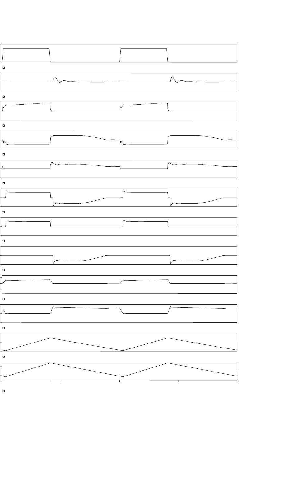
Figure 10.30 shows the waveforms of the forward converter
(circuit given in Fig. 10.28) when ultra-fast diodes are used as
D
M
, D
R
, and D
F
. (Note that ultra-fast diodes are actually much
slower than Schottky diodes.) The waveforms are obtained by
PSpice simulations, based on the following assumptions:
• D
M
is an MUR460 ultra-fast diode. D
R
and D
F
are
MUR1560 ultra-fast diodes.
• M
1
is an IRF640 MOS transistor.
• Transformer T
1
has a coupling coefficient of 0.99999999
(which may be assumed to be 1).
• The switching operation of the converter has reached a
steady state.

166 Y. S. Lee and M. H. L. Chow
V(99)
3.6V
3.7V
I(L1)
5A
10A
15A
I(DF)
–100A
0A
100A
I(DR)
–100A
0A
100A
V(6,9)
–20V
0V
20V
V(9)
–20V
0V
20V
V(6)
–20V
0V
20V
V(3)
–200V
0V
200V
V(100)
–100V
0V
100V
ID(M1)
–40A
0A
40A
I(DM)
–500mA
0A
500mA
V1(VPULSE)
0V
20V
Time
0s
4us
DT
5us
10us
T
15us 20us
ON OFF ON OFF
DT T
3.8V
FIGURE 10.30 Waveforms of forward converter using “ultra-fast” diodes (which are actually much slower than Schottky diodes).

10 Diode Rectifiers 167
It is observed that a large spike appears in the current wave-
forms of diodes D
R
and D
F
(denoted as I(DR) and I(DF)
in Fig. 10.30) whenever the MOS transistor M
1
is turned
on. This is due to the relatively slow reverse recovery of the
flywheel diode D
F
. During the reverse recovery time, the pos-
itive voltage suddenly appearing across L
S
(which is equal to
V
IN
(N
S
/N
P
)) drives a large transient current through D
R
and
D
F
. This current spike results in large current stress and power
dissipation in D
R
, D
F
, and M
1
.
A method of reducing the current spikes is to use Schottky
diodes as D
R
and D
F
, as described below.
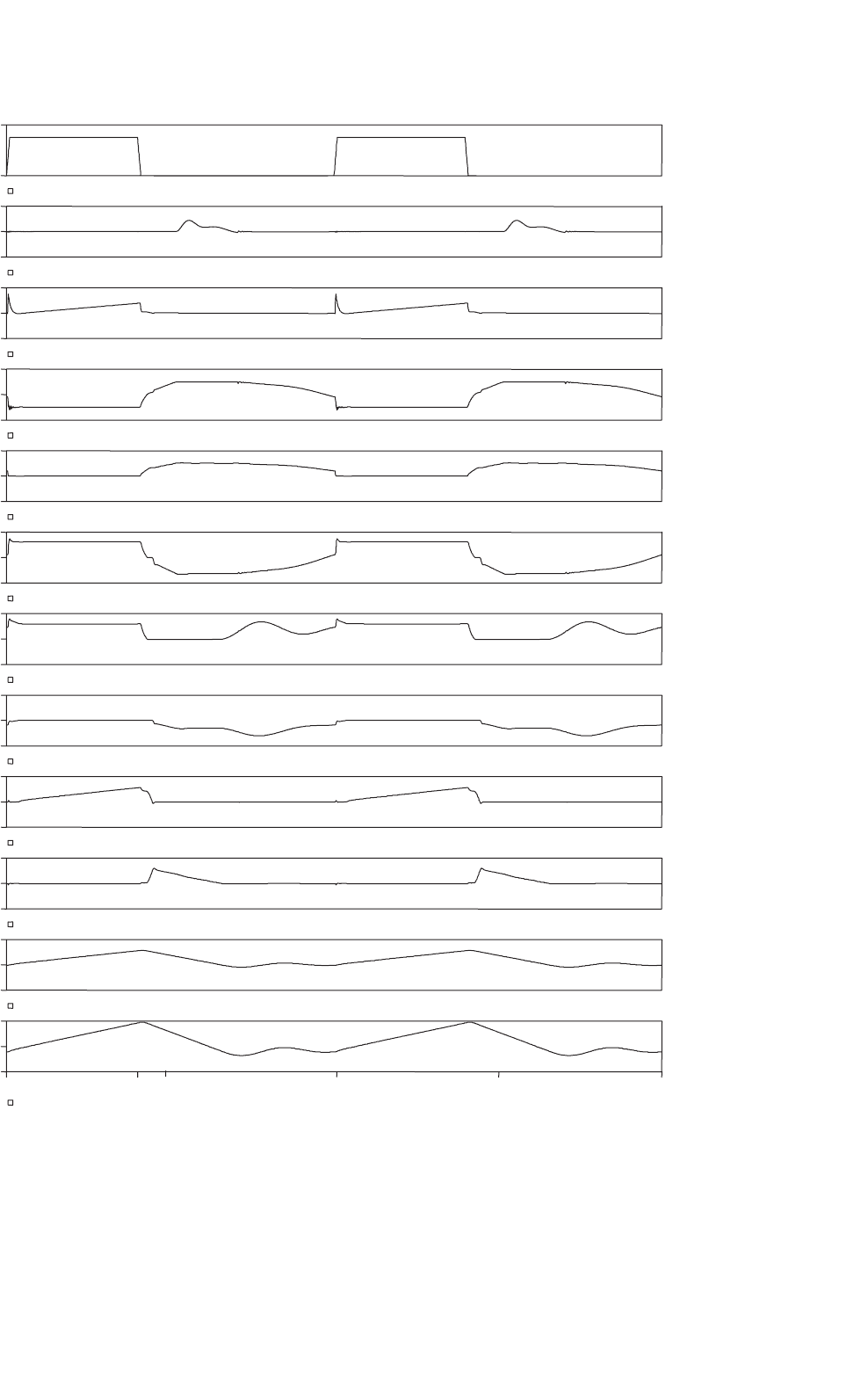
10.6.1.3 Circuit Using Schottky Diodes
In order to reduce the current spikes caused by the slow reverse
recovery of rectifiers, Schottky diodes are now used as D
R
and
D
F
.The assumptions made here are (referring to the circuit
shown in Fig. 10.28):
• D
R
and D
F
are MBR2540 Schottky diodes.
•
D
M
is an MUR460 ultra-fast diode.
• M
1
is an IRF640 MOS transistor.
• Transformer T
1
has a coupling coefficient of 0.99999999.
• The switching operation of the converter has reached a
steady state.
The new simulated waveforms are given in Fig. 10.31. It is
found that, by employing Schottky diodes as D
R
and D
F
, the
amplitudes of the current spikes in ID(M1), I(DR), and I(DF)
can be reduced to practically zero. This solves the slow-speed
problem of ultra-fast diodes.
10.6.1.4 Circuit with Practical Transformer
The simulation results given above in Figs. 10.29–10.31 (for
the forward converter circuit shown in Fig. 10.28) are based
on the assumption that transformer T1 has effectively no leak-
age inductance (with coupling coefficient K = 0.99999999).
It is, however, found that when a practical transformer
(having a slightly lower K ) is used, severe ringings occur.
Figure 10.32 shows some simulation results to demonstrate
this phenomenon, where the following assumptions are made:
• D
R
and D
F
are MBR2540 Schottky diodes. D
M
is an
MUR460 ultra-fast diode.
• M
1
is an IRF640 MOS transistor.
• Transformer T
1
has a practical coupling coefficient of
0.996.
•
The effective winding resistance of L
P
is 0.1 . The effec-
tive winding resistance of L
M
is 0.4 . The effective
winding resistance of L
S
is 0.01 .
• The effective series resistance of the output filtering
capacitor is 0.05 .
• The switching operation of the converter has reached a
steady state.
The resultant waveforms shown in Fig. 10.32 indicate that
there are large voltage and current ringings in the circuit.
These ringings are caused by the resonant circuits formed by
the leakage inductance of the transformer and the parasitic
capacitances of diodes and transistor.
A practical converter may therefore need snubber circuits
to damp these ringings, as described below.
10.6.1.5 Circuit with Snubber Across the
Transformer
In order to suppress the ringing voltage caused by the res-
onant circuit formed by transformer leakage inductance and
the parasitic capacitance of the MOS switch, a snubber circuit,
shown as R
1
and C
1
in Fig. 10.33, is now connected across the
primary winding of transformer T
1
. The new waveforms are
shown in Fig. 10.34. Here the drain-to-source voltage wave-
form of the MOS transistor, V(3), is found to be acceptable.
However, there are still large ringing voltages across the output
rectifiers (V(6,9) and V(9)).
In order to damp the ringing voltages across the output
rectifiers, additional snubber circuits across the rectifiers may
therefore also be required in a practical circuit, as described
below.
10.6.1.6 Practical Circuit
Figure 10.35 shows a practical forward converter with snubber
circuits added also to rectifiers (R
2
C
2
for D
R
and R
3
C
3
for D
F
) to reduce the voltage ringing. Figures 10.36 and
10.37 show the resultant voltage and current waveforms.
Figure 10.36 is for continuous-mode operation (R
L
= 0.35 ),
where I(L1) (current in L
1
) is continuous. Figure 10.37 is
for discontinuous-mode operation (R
L
= 10 ), where I(L1)
becomes discontinuous due to an increased value of R
L
. These
waveforms are considered to be acceptable.
The design considerations of diode rectifier circuits in
high-frequency converters will be discussed later in Sub-
section 10.6.3.
10.6.2 Flyback Rectifier Diode and Clamping
Diode in a Flyback Converter
10.6.2.1 Ideal Circuit
Figure 10.38 shows the basic circuit of a flyback converter. Due
to its simple circuit, this type of converter is widely used in low-
cost low-power applications. Discontinuous-mode operation
(meaning that the magnetizing current in the transformer falls
to zero before the end of each switching cycle) is often used
because it offers the advantages of easy control and low diode
reverse-recovery loss. Figure 10.39 shows the idealized steady-
state waveforms for discontinuous-mode operation. These
waveforms are obtained from PSpice simulations, based on

168 Y. S. Lee and M. H. L. Chow
V(99)
4.7V
4.8V
4.9V
I(L1)
10A
15A
20A
I(DF)
–20A
0A
20A
I(DR)
–20A
0A
20A
V(6,9)
–20V
0V
20V
V(9)
–20V
0V
20V
V(6)
–20V
0V
20V
V(3)
–200V
0V
200V
V(100)
–100V
0V
100V
ID(M1)
–5.0A
0A
5.0A
I(DM)
–500mA
0A
500mA
V1(VPULSE)
0V
20V
Time
0s
4us
DT
5us
10us
T
15us 20us
ON OFF ON OFF
DT T
FIGURE 10.31 Waveforms of forward converter using Schottky (fast-speed) diodes as output rectifiers.

10 Diode Rectifiers 169
V(99)
4.1V
4.2V
I(L1)
10.0A
12.5A
15.0A
I(DF)
–20A
0A
20A
I(DR)
–20A
0A
20A
V(6,9)
–100V
0V
100V
V(9)
–40V
0V
40V
V(6)
–100V
0V
100V
V(3)
–400V
0V
400V
V(100)
–400V
0V
400V
ID(M1)
–4.0A
0A
4.0A
I(DM)
–4.0A
0A
4.0A
V1(VPULSE)
0V
20V
Time
0s
4us
DT
5us
10us
T
15us 20us
ON OFF ON OFF
DT T
FIGURE 10.32 Waveforms of forward converter with practical transformer and output filtering capacitor having non-zero series effective resistance.

170 Y. S. Lee and M. H. L. Chow
V
IN
= 50 V, D
M
= MUR460
D
R
= MBR2540, D
F
= MBR2540
M
1
= IRF640, R
1
= 24 W
C
1
= 3000 pF, C
L
= 3500 mF
ESR of C
L
= 0.05 W, L
1
= 8 mH
L
P
= 0.576 mH, L
M
= 0.576 mH
L
S
= 0.036 mH, N
P
: N
M
: N
S
= 4 : 4 : 1
R
L
= 0.35 W
Effective winding resistance of L
P
=0.1 W
Effective winding resistance of L
M
=0.4 W
Effective winding resistance of L
S
= 0.01 W
Coupling coefficient K = 0.996
Pulse
2
6
0
99
1
3
5
100
0
D
M
D
R
D
F
C
L
C
1
R
1
R
L
V
IN
L
S
N
S
L
P
N
P
L
M
N
M
M
1
T
1
L
1
9
V
o
FIGURE 10.33 Forward converter with snubber circuit (R
1
C
1
) across transformer.
the following assumptions:
• D
R
is an idealized rectifier diode with infinitely fast
switching speed.
• M
1
is an idealized MOS switch with infinitely fast
switching speed and
On-state resistance = 0.067
Off-state resistance = 1M
• Transformer T
1
has a coupling coefficient of 0.99999999.
•
The switching operation of the converter has reached a
steady state.
Referring to the circuit shown in Fig. 10.38 and the wave-
forms shown in Fig. 10.39, the operation of the converter can
be explained as follows:
1. For 0 < t < DT
The switch M
1
is turned on at t = 0.
V
(
3
)
= 0 for 0 < t < DT
The current in M
1
, denoted as ID(M1), increases at
the rate of
dID(M 1)
dt
=
V
IN
L
P
(10.99)
The output rectifier D
R
is reversely biased.
2. For DT < t < (D+D
2
)T
The switching M
1
is turned off at t = DT.
The collapse of magnetic flux induces a back emf
in L
S
to turn-on the output rectifier D
R
. The initial
amplitude of the rectifier current I(DR), which is also
denoted as I(LS), can be found by equating the energy
stored in the primary-winding current I(LP) just before
t = DT to the energy stored in the secondary-winding
current I(LS) just after t = DT:
1
2
L
P
[
I
(
LP
)
]
2
=
1
2
L
S
[
I
(
LS
)
]
2
(10.100)
1
2
L
P
V
IN
L
P
DT
2
=
1
2
L
S
[
I
(
LS
)
]
2
(10.101)
I
(
LS
)
=
L
P
L
S
V
IN
L
P
DT (10.102)
I
(
LS
)
=
N
P
N
S
V
IN
L
P
DT (10.103)
The amplitude of I(LS) falls at the rate of
dI
(
LS
)
dt
=
−V
o
L
S
(10.104)
and I(LS) falls to zero at t =(D+D
2
)T. Since D
2
V
o
=
V
IN
(N
S
/N
P
)D
D
2
=
V
IN
V
o
N
S
N
P
D (10.105)
D
2
is effectively the duty cycle of the output rectifier
D
R
.
3. For (D + D
2
)T < t < T
The output rectifier D
R
is off.
The output capacitor C
L
provides the output current
to the load R
L
.
The switching cycle restarts when the switch M
1
is
turned on again at t = T.
From the waveforms shown in Fig. 10.39, the fol-
lowing information (for discontinuous-mode operation)

10 Diode Rectifiers 171
V(99)
4.1V
4.2V
I(L1)
10.0A
12.5A
15.0A
I(DF)
–20A
0A
20A
I(DR)
–20A
0A
20A
V(6,9)
–40V
0V
40V
V(9)
–40V
0V
40V
V(6)
–50V
0V
50V
V(3)
–200V
0V
200V
V(100)
–100V
0V
100V
ID(M1)
–4.0A
0A
4.0A
I(DM)
–1.0A
0A
1.0A
V1(VPULSE)
0V
20V
Time
0s
4us
DT
5us
10us
T
15us 20us
ON OFF ON OFF
DT T
FIGURE 10.34 Waveforms of forward converter with snubber circuit across the transformer.

172 Y. S. Lee and M. H. L. Chow
VIN = 50 V, D
M
= MUR460
D
R
= MBR2540, D
F
= MBR2540
M
1
= IRF640, R
1
= 24 W
R
2
= 10 W, R
3
= 10 W
C
1
= 3000 pF, C
2
= 10 nF, C
3
= 10 nF
C
L
= 3500 mF, ESR of C
L
= 0.05 W
L
1
= 8 mH, L
P
= 0.576 mH
L
M
= 0.576 mH, L
S
= 0.036 mH
N
P
: N
M
: N
S
= 4: 4 : 1
Effective winding resistance of L
P
= 0.1 W
Effective winding resistance of L
M
= 0.4 W
Effective winding resistance of L
S
= 0.01 W
Coupling coefficient K = 0.996
Pulse
2
6
0
99
69
90
1
3
5
100
0
D
M
D
R
D
F
C
L
R
L
C
1
C
3
C
2
R
1
R
3
R
2
V
IN
L
S
N
S
L
P
N
P
L
M
N
M
M
1
T
1
L
1
9
V
o
FIGURE 10.35 Practical forward converter with snubber circuits across the transformer and rectifiers.
can be obtained:
• The maximum value of the current in the switch M
1
is
ID(M1)
max
=
V
IN
L
P
DT (10.106)
• The maximum value of the current in the output rectifier
D
R
is
I
(
DR
)
max
=
N
P
N
S
V
IN
L
P
DT (10.107)
• The output voltage V
o
can be found by equating the input
energy to the output energy within a switching cycle.
V
IN
×[Charge taken from V
IN
in a switching cycle]
=
V
2
o
R
L
T
V
IN
1
2
DT
DT
L
P
V
IN
=
V
2
o
R
L
T (10.108)
V
o
=
R
L
T
2L
P
DV
IN
(10.109)
• The maximum reverse voltage of D
R
, V(6,9) (which is
the voltage at node 6 with respect to node 9), is
V
(
DR
)
max
= V
(
6, 9
)
max
= V
IN
N
S
N
P
+V
o
(10.110)
10.6.2.2 Practical Circuit
When a practical transformer (with leakage inductance) is used
in the flyback converter circuit shown in Fig. 10.38, there will
be large ringings. In order to reduce these ringings to prac-
tically acceptable levels, snubber and clamping circuits have
to be added. Figure 10.40 shows a practical flyback converter
circuit where a resistor–capacitor snubber (R
2
C
2
) is used to
damp the ringing voltage across the output rectifier D
R
, and a
resistor–capacitor-diode clamping (R
1
C
1
D
S
) is used to clamp
the ringing voltage across the switch M
1
. What the diode D
S
does here is to allow the energy stored by the current in the
leakage inductance to be converted to the form of a dc voltage
across the clamping capacitor C
1
. The energy transferred to
C
1
is then dissipated slowly in the parallel resistor R
1
, without
ringing problems.
The simulated waveforms of the flyback converter (circuit
given in Fig. 10.40) for discontinuous-mode operation are
shown in Fig. 10.41, where the following assumptions are
made:
• D
R
and D
S
are MUR460 ultra-fast diodes.
• M
1
is an IRF640 MOS transistor.
• Transformer T
1
has a practical coupling coefficient of
0.992.
• The effective winding resistance of L
P
is 0.025 . The
effective winding resistance of L
S
is 0.1 .
• The effective series resistance of the output filtering
capacitor C
L
is 0.05 .
• The switching operation of the converter has reached a
steady state.
The waveforms shown in Fig. 10.40 are considered to be
acceptable.
10.6.3 Design Considerations
In the design of rectifier circuits, it is necessary for the designer
to determine the voltage and current ratings of the diodes. The
idealized waveforms and expressions for the maximum diode
voltages and currents given under the heading of “Ideal cir-
cuit” above (for both forward and flyback converters) are a
good starting point. However, when parasitic/stray compo-
nents are also considered, the simulation results given under
10 Diode Rectifiers 173
V(99)
4.1V
4.2V
I(L1)
10.0A
12.5A
15.0A
I(DF)
–20A
0A
20A
I(DR)
–20A
0A
20A
V(6,9)
–20V
0V
20V
V(9)
–20V
0V
20V
V(6)
–20V
0V
20V
V(3)
–200V
0V
200V
V(100)
–100V
0V
100V
ID(M1)
–4.0A
0A
4.0A
I(DM)
–1.0A
0A
1.0A
V1(VPULSE)
0V
20V
Time
0s
4us
DT
5us 10us
T
15us
20us
ON OFF ON OFF
DT T
FIGURE 10.36 Waveforms of practical forward converter for continuous-mode operation.
174 Y. S. Lee and M. H. L. Chow
V(99)
7.4V
7.5V
7.6V
I(L1)
–4.0A
0A
4.0A
I(DF)
–4.0A
0A
4.0A
I(DR)
–4.0A
0A
4.0A
V(6,9)
–40V
0V
40
V(9)
–20V
0V
20V
V(6)
–20V
0V
20V
V(3)
–200V
0V
200V
V(100)
–100V
0V
100V
ID(M1)
–2.0A
0A
2.0A
I(DM)
–500mA
0A
500mA
V1(VPULSE)
0V
20V
Time
0s
4us
DT
5us
10us
T
15us 20us
ON OFF ON OFF
DT T
FIGURE 10.37 Waveforms of practical forward converter for discontinuous-mode operation.