Hughes M.P., Hoettges K.F. (Eds.) Microengineering in Biotechnology
Подождите немного. Документ загружается.

l
The characteristic times to polarize the membrane from the
outside or the inside are well separated in the spectrum.
l
The resulting forces on the particles are larger due to the
Clausius–Mausotti factor but also because larger electric fields
can be applied without generating heating and convective
flows.
l
Positive and negative DEP can both be induced for different
excitation frequencies.
In AC electrokinetic techniques, measurement or separation are
based on the cell motile response to the electric field and thus
uncontrolled pressure or thermally induced flow (and for smaller
particles Brownian motion) can be considered as noise. For cell
sized particles the observable measurement noise in terms of
Brownian motion can be neglected at room temperature and
clearly does not depend on the liquid conductivity.
In ROT, other sources of measurement uncertainty exist,
although not directly related to solution conductivity. Rotation
rate can be influenced by adhesion between the cell and substrate
or by dipole–dipole interactions of nearby cells. At low frequency,
ROT measurements are also complicated by electroosmosis effects
whereby the electric field rotates the double layer and hence the
fluid around the particle.
4.4.2. AC Dielectric
Spectroscopy
In AC dielectric spectroscopy, it is more difficult to answer the
question of medium composition based only on the electrical prop-
erties of the sample because the detection circuit plays an important
role in the determination of the sensitivity of the instrument.
Although a low conductivity medium increases the separation
between the two Maxwell-Wagner dispersions in the spectrum
as shown in Fig. 7.10, the resistance of the detection volume
could well reach the M range. This has number of important
consequences:
l
Higher Johnson noise is expected for low conductivity media.
l
Measurement in the MHz range circuits for high impedance
values are difficult to implement; the electronic and sensor are
much more sensitive to parasitic capacitances.
l
The fraction of conductive current in the system is significantly
reduced whereas the dielectric current increases.
l
To evaluate the total drop in permittivity in a low conductivity
medium, data have to be acquired over a frequency band about
twice as broad to find the low and high frequency values of the
suspension permittivity and conductivity.
l
If the cell to be measured is only present in the measurement
electric field for a few milliseconds, then measurements done
at the lower end of the frequency spectrum will be not have
time to reach equilibrium.
166 Gawad et al.

This comparison between the two approaches seems to indicate
that for AC dielectric spectroscopy, using low conductivities is not
as beneficial as it is in the case of AC electrokinetics.
5. Cell
Manipulation in
Streams
Isolation and positioning of cells in a microfluidic channel by means
of micromanipulation is essential if one is to obtain consistent results
from the device. To reproducibly measure the particle electrical
properties the system must be able to transport the sample solution
precisely to and through specific locations within the chip. By redu-
cing the fluidic channel dimensions, sequential tracking of each
particle passing through the system detection area is made possible.
The flow rate should be held constant over the duration of the
experiment. Accurate speed control and the option to stop or
reverse the flow are desirable functionalities and are relatively
easy to implement using external pressure or flow controllers. By
varying the cross-section of the flow channel consecutive system,
components (e.g., DEP focusing, impedance detection, sorting)
can be integrated along the pathway that the cells take through the
device, each requiring locally different flow and particle speeds.
A number of liquid pumping mechanisms applicable to micro-
systems are described in the literature, which can be separated into
bulk and surface effects. Pressure-driven flow (PDF) is the simplest
implementation for bulk techniques. The driving pressure can be
generated outside of the chip with pumps or pressure regulators
connected by short lengths of small bore tubing to minimize the
compliance of the fluidics of the system as well as maintain sufficient
flow in the sample supply tube to minimize sedimentation effects. A
simple and precise method consist of priming the system and adjust-
ing the height of a water column either up-stream or down-stream
of the chip. Other techniques have been developed to exert pressure
directly on the liquid inside the chip using piezoelectric pumping
(35), centrifugal force (36), or thermal expansion (37).
Microfabricated chips allow the use of negative dielectrophor-
esis (nDEP) as a method to control the trajectories of particles and
cells within the fluidic microchannel. Pairs of planar, overlapped
top and bottom electrode strips are used to produce high electric
field gradients within the liquid. The resulting force on the particle
is proportional to the gradient of the electric field intensity squared
and to the particle polarizability. In nDEP particles tend to move
toward regions of lower electric field intensity. The electrodes are
designed with a defined angle to the flow direction (Fig. 7.11).
When entering the locally generated electric field, the particles
moving under the influence of the PDF are subject to the nDEP
Impedance Spectroscopy, Optical Analysis of Single Biological Cells 167

force acting perpendicular to the electrode strips. The Stokes force,
from the fluid, can be separated into two components. The first,
parallel to the electrodes, tends to move the particles along the
electrodes edge. The second, perpendicular to the strip electrode,
tends to push the particle into the electric field gradient and oppose
the DEP force until the particle arrives at an equilibrium position a
certain distance from the electrode edge. If the Stokes force is too
large and force equilibrium is not reached, the particle will enter the
electric field deeper and potentially cross the nDEP barrier.
A discussion of the nDEP and Stokes force on a particle as a
function of the barrier angle to the fluid flow is given by Du¨rr
et al.(38) and Schnelle et al. (39), using the expressions
F
DEP
¼
27
32
p
2
"
1
Re½
~
KR
3
U
2
rms
h
3
; [13]
F
Stokes
¼ 6pRv: [14]
The particles are deflected by the barrier for F
DEP
4
F
Stokes
sin ,
which gives a maximal speed v
max
Fig. 7.11. Schematic of the chip bottom half structure showing the different electrodes
functions and the electric and fluidic interface. A number of electrodes are unexploited or
redundant in the impedance spectroscopy design, but can be used in other applications.
168 Gawad et al.

v
max
¼
9p"
1
Re½
~
K
64
R
2
U
2
rms
h
3
sin
; [15]
where R is the particle radius, U
rms
is the root mean square of the
electric voltage applied between the electrodes, and h is the chan-
nel height.
In current chip designs, the fluidic channel is wider in the nDEP
regions (100–200 mm) than in the detection part of the system in
order to reduce the flow speed and applied nDEP electric field. The
nDEP electrode are 8 mm wide, which is a compromise between
limitations of fabrication technology, the need for a high electric
field gradient, and minimization of Joule heating in the channel.
A vertical component of the DEP force is also observed. Its effect
is particularly visible on particles whose trajectories are initially close
to the bottom surface of the channel. As the particles get close to the
bottom electrode edge, they are swiftly pushed upward in the flow
and their speed increases as they enter faster flow lines. As they move
to faster lines, the particles experience a larger Stokes force and enter
the barrier field more deeply and thus end up more centered. The
final particle equilibrium position and particularly its height in the
channel is thus a function of the Stokes, sedimentation, and nDEP
forces. The estimated time constant for this effect is observed for the
acceleration of slow particles as they move from the channel walls to
the central flow axis and is on the order the order of a 100 ms. It
should be in principle similar to what is observed in DEP-FFF (40).
Figure 7.11 shows the layout of a typical microfluidic chip
including a DEP focusing area followed by a pair of measurement
electrodes placed between ground shielding electrodes in a nar-
rower channel section. A set of electrodes is added at the exit of the
measurement channel to allow sorting of the particles toward one
fluidic outlet or the other based on their measured properties (41).
To accommodate different chip fluidic configurations, the
fluidic access to the chip or ‘‘holes’’ are defined on a grid with
the possibility for three inlets and three outlets. Figure 7.12
shows dual inlet and triple inlet configurations illustrating the
flexibility of the fluidic system.
ab
Fig. 7.12. Dual input (a) and sheath flow (b) options demonstrating the flexibility of the fluidic setup for pressure-driven
flow control. (Images courtesy of N. Demierre and U. Seger.)
Impedance Spectroscopy, Optical Analysis of Single Biological Cells 169
6. Chip Fabrication
Process
Several techniques may be used to produce capillary channels in
the micrometer size range, but in order to be able to accurately
position electrodes on opposed channel walls the aligned sandwich
technique was used.
Glass substrates were used (100 mm in diameter and 700 mm
thick, Schott-Guinchard, Switzerland). The wafers are optically
polished to l/10 for Ø 5 mm and the surface roughness is speci-
fied below 5 A
˚
.
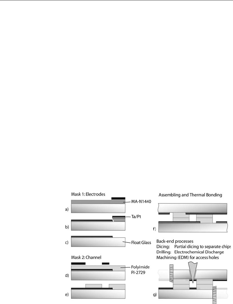
The first deposited layer consists of a thin metal film structure
which is patterned by lift-off using either a reversible photoresist
the AZ-5214 (Clariant) or the ma-N1440 (micro resist technol-
ogy) which does not require an inversion bake (Fig. 7.13a). The
sputtered electrode material consists of tantalum or titanium
(20 nm), as an adhesion layer, and platinum (200 nm) as the active
electrode material (Fig. 7.13b). Both layers were sputtered in
vacuum using a Balzers 450. The deposition rate is set to
0.3 nm s
–1
. Lift-off is done in an ultrasonic acetone bath at
25C, followed by an isopropanol rinse (Fig. 7.13c).
A thick photosensitive polyimide precursor (PI 2729,
Dupont) is used to define the channels. It is spun over the pat-
terned electrodes at a final speed of 4,000 rpm. A preliminary
Fig. 7.13. Process flow for the microfluidic chip. (a–c) Patterning of the microelectrodes
by lift-off. (d–e) Patterning of channel walls with photosensitive polyimide precursor.
(f) Sealing of the channels by flip-chip alignment of the patterned wafer structures and
thermal bonding. (g) Double side partial dicing to separate the chips and provide
electrode contact access. Electrochemical discharge machining is used to open the
access holes.
170 Gawad et al.

adhesion promoter dipping (VM-651, Dupont) is used to prevent
edge detachment of the polyimide layer at development. A soft
bake step of 5 min at 60C followed by a 5 min at 100Cis
performed prior to the layer exposure. Photolithography is done
in hard contact mode and the exposure parameters are 40 s at 10
mW cm
–2
(MA-6, Karl-Suss, Fig. 7.13d). The polyimide devel-
opment process (Fig. 7.13e) is repeated three times in a cycle of
three consecutive baths of 100% developer (DE6180, Dupont),
50–50% developer and rinse mixture and 100% rinse (RI9180,
Dupont), 30 s in each bath and maintaining constant agitation.
A final rinse is performed in a fresh rinse solution and development
is checked optically. As two identical wafers will be put face-to-face
to build a complete chip, the polyimide layer on each chip repre-
sents half of the final channel height.
The alignment of the two facing wafers is performed with a
bond aligner (BA-6, Karl-Suss), with an estimated alignment
precision of 2–3 mm. The thermal bonding (SB-6, Karl-Suss,
Fig. 7.13f) of the facing polyimide layers is done under a tool
pressure of 5 bars and by ramping the temperature to 200C
for a bake of 30 min in air and followed by 300CinN
2
for 1h
(Fig. 7.14). The first bake is performed in order to degrade the
photo-package with oxygen, as it is known to migrate to the
polyimide surface and prevent adhesion between the two layers.
At higher temperature, an inert atmosphere is maintained to pre-
vent oxidation of the polyimide, which is otherwise observed as
darkening of the polymer layer after bonding.
Another aspect of the polyimide–polyimide bonding process is
the significant degassing and consequent volume reduction that
occurs during curing. The thickness of the layer after the thermal
Fig. 7.14. Two bonded wafers containing 21 chips. Dicing and drilling are then performed
to obtain individual functional devices.
Impedance Spectroscopy, Optical Analysis of Single Biological Cells 171

bonding procedure is only 50% of the originally spun precursor.
Degassing is responsible for the formation of bubbles at the inter-
face between the polyimide layers. To allow these byproducts to
vent, a venting grid is used around the fluidic channels. The design
of this grid is such that measurement and DEP electrodes are
covered by polyimide everywhere except in the channel and elec-
trical contact areas. The final operations consist of the back-end
processes performed in a grey room and include partial chip dicing
in order to access the electrode contacts on each side of the chip
and electrochemical discharge machining to drill the fluidic access
holes (Fig. 7.13 g) (42).
The electrochemical access hole drilling process is shown in
Fig. 7.15. With the wafer scale polyimide bonding, this operation
represents one of the most critical step in the chip manufacturing
a
b
Fig. 7.15. Principle of glass electrochemical etching (a) and view of a microfluidic chip
with electrochemically etched access holes (b). The chip is placed in a 30% NaOH
solution. Electrical discharges are produced at a tip of a steel electrode which etches the
glass at a rate of 20 mms
–1
.
172 Gawad et al.

as glass debris and other particles can enter and obstruct the
microfluidic channels. Ultrasonic and PDF cleaning using differ-
ent liquid viscosities can be used in cases where debris has entered
the channels and generally permits 100% recovery of the chips.
Alternative techniques would be required in order to indus-
trialize this process, allowing mass production of such devices. A
possible approach would be to define the channel walls on a single
wafer and to drill holes on the second prior to bonding.
6.1. Experimental
Setup
A fluidic block composed of two mechanical parts is used to hold
the chip in the center of the amplification electronics circuit board
Fig. 7.16. The bottom part of the block is screwed to the printed
circuit board and allows for precise placement of the chip. Two
interface connectors each with 15 gold plated spring contacts
(Samtec, 1 mm pitch) are used to contact the top and bottom of
the platinum electrodes. Compared to other techniques, such as
wire bonding or soldering, replacing the chip in the setup is very
fast, requires no tools, and gives excellent reproducibility.
The top part is made of PEEK, which is resistant to solvents
and bleach (Fig. 7.17). It provides L-shaped conduits to the chip
fluidic apertures and the top side electrical connections to the chip.
The fluidic contact is made watertight using miniature o-rings.
The tubing connection to the fluidic block uses standard NPT 28
1/16 connectors. Additionally, an aperture is made in the center
of the top block for non-fluorescent illumination of the chip.
Fig. 7.16. The chip is placed in the PEEK electro-fluidic interconnection block. The top
and bottom electrical connections are provided by two rows of 15 spring-loaded
contacts. Optical access and transmissive illumination are provided through holes in
the printed circuit board and block.
Impedance Spectroscopy, Optical Analysis of Single Biological Cells 173

A rotary valve selects the different washing or priming liquids,
which are contained in pressurized bottles. Additionally, a motor-
ized syringe pump is used for fast purging of the whole line with
high pressure and proved very useful in case of channel clogging.
The tubing inner diameter in the sample path is 120 mm, while it is
1 mm for the purging and washing liquids. The sample holder
tubing to the fluidic block is made as short as possible in order to
avoid cell sedimentation in the tubing. The holder supports stan-
dard 5 ml falcon tubes and provides sample agitation functionality to
avoid sedimentation as well as optional temperature control. A valve is
placed just before the fluidic block to select between cleaning liquid
and sample. An inlet-side waste provides for a way to quickly purge
the entry lines without having to remove the chip. Pressure control of
the sample tube is provided by a high-precision pressure regulator
(Marsh-Bellofram), with full scale pressure of 10 psi (0.7 bar), for ten
turns. The regulator allows precise control of the fluid flow and is
sufficient to stop the flow and particles even in the smallest part of the
microchannel. The time constant of the system fluidics is estimated
to be below 0.2 s. The height and level of the liquid in the
collection vials is set so as to produce a small back-flow when
atmospheric pressure is applied on the sample.
7. Measurements
and Results
The primary aim of this section is to demonstrate that such a
system can discriminate particles according to their dielectric and
optical properties. We illustrate the efficacy of the system with the
Fig. 7.17. Fluidic setup. The different washing liquids are either volume or pressure
driven. The desired liquid or sample can be directed to the fluidic block through rotary
valves. Miniature o-rings provide quick and water-tight fluidic connection to the chip.
Waste vials are available before or after the chip for tube purging and fast sample
injection.
174 Gawad et al.

example of algae species discrimination. However, to test the
system sensitivity, a number of preliminary experiments based on
simple non-biological models are regularly performed. These steps
are useful in defining or verifying a number of measurement para-
meters such as particles’ flow speed, filters, or gain settings, which
influence the measurements.
The calibration test is performed on the impedance spectro-
scopy instrument using beads of three different sizes, with diameters
of 4.0 mm, and 6.0 mm (Duke scientific), and 5.14 mm (Molecular
probes), which are mixed in the same sample tube. In Fig. 7.18,
they are designated as 4, 5.14, and 6 mm beads. The coefficient of
variation (CV) of the particles measured with a commercial FACS,
the microfabricated impedance chip and those given by the bead
manufacturers are summarized in Table 7.1.
Sub-micron size differentiation using calibrated polystyrene
beads is thus easily achieved with such a system.
A number of measurements have previously demonstrated the
application of such a system in the field of haematology and
immunology. Published work also shows differentiation between
red blood cells and red blood cell ghosts fixed with glutaraldehyde
at various concentrations (43).
More recently, preliminary data using the impedance spectro-
scopy flow cytometry system shows the possibility of discrimina-
tion between neutrophils (granular, 12–15 mm diameter, multi-
lobed nucleus), lymphocytes (5–10 mm, large nucleus), and
monocytes (12–18 mm, U-shaped nucleus). Lymphocytes can be
Fig. 7.18. Size-calibrated bead data as measured in PBS at 3 MHz using the integrated
impedance sensor. Simple analysis of the signal shape of the dots outside the three main
clouds showed they were due to doublets and were discarded for CV calculations.
Impedance Spectroscopy, Optical Analysis of Single Biological Cells 175