Hughes M.P., Hoettges K.F. (Eds.) Microengineering in Biotechnology
Подождите немного. Документ загружается.


well-characterized machines, a well-defined fabrication process,
well-designed photomasks, and careful fabrication. To maximize
the possibility of success, it is highly recommended that the novice
microfabricator devote a great deal of time to designing the device
and process before beginning production. Properly designed
photomasks and a complete process run sheet, or traveler, can be
assembled by talking with people familiar with the process tools
available in the laboratory. This simply a list of all the processes and
their many variables in the proper order, and a simple example is
given below. In the world of microfabrication, the tiniest of details
can determine the success or failure of a project, so a concise record
of all the processing is necessary to repeat a successful process.
It is this author’s experience that new scientists, biologists, and
engineers building their first microdevice typically expect the first
attempt at fabrication to work. This is rarely the case, so one
should expect several scrap wafers before having success. The
reason is that in a research setting, well-characterized, reproduci-
ble, standardized processes are not often available, and as Mur-
phy’s law states, anything that can go wrong will. With hundreds
of variables to control, and only limited knowledge of any given
process step, fabricating a device correctly during the first attempt
is not highly probable. An engineer or biologist must fabricate the
device under the limitations of the laboratory equipment available
and the time available to characterize processes, but the resources
available to the researcher limit processing capabilities.
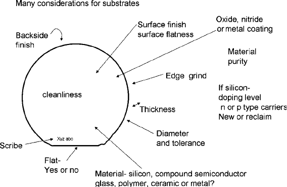
2. Substrates
The first consideration for microfabrication is the substrate,or
wafer, the device will be built upon. Integrated circuits are built
on wafers, where micromachines can be built on a variety of sub-
strate materials, so the term substrate is used interchangeably with
wafer. Micromachining is often divided into two categories, bulk
and surface. In bulk micromachining, the substrate is formed into
the finished device, whereas in surface micromachining layers are
added on top (or on the bottom) of the substrate, and the added
layers are formed into the desired device. Many technologies
combine surface and bulk micromachining. It is highly recom-
mended that one obtain many more substrates than are required
for the project to use as dummy wafers, test wafers and to take into
account scrapped wafers caused by misprocessing. Plan on drop-
ping and breaking some substrates too. It is also recommended
that substrates be scribed at the beginning of the process to make
traceability easier. The variables affecting the specification of
substrates can be seen in Fig.1.1.
4 Chinn
The selection of a substrate determines much of the
subsequent processing. Most microfabrication tools are designed
for silicon wafers with a flat. The flat is simply an area ground off of
the edge of the round wafer. It is there so that the crystal orienta-
tion can be determined and is used by automated processing
equipment to orient the wafer. Square or other shaped substrates
can be used, but non-circular substrates are much harder to work
with and do not fit in many machines. Round substrates spin much
better than squares do. Most laboratories have one or two standard
sizes that fit into most machines, so it is advantageous to use a
standard size. Two-inch (50 mm), three-inch (75 mm), four-inch
(100 mm), and six-inch (150 mm) substrates are common stan-
dards. However, the metric and English sizes are not necessarily
compatible in some machine wafer holders (1 inch=25.4 mm).
When ordering substrates, several variables must be accounted
for. After diameter, and thickness, one must determine the flat-
ness, surface roughness, edge grind, the finish on the back of the
substrate, temperature limitations, coefficient of thermal expan-
sion, and transparency to a given wavelength of light and
mechanical toughness. Poorly ground edges can be a source of
particles when they chip, and can initiate cracks which will cause
the substrate to break. In a plasma etch process, note that the
conductivity of the substrate can have an impact on the way the
material etches.
Silicon has the advantage that it is widely available, relatively
inexpensive and very well characterized. It is also the most perfect
material obtainable, being a slice of a single crystal. The crystal-
linity can be taken advantage of in directional etches and in
Fig. 1.1. The selection and specifications of the substrate to be used are critical variables
that can determine how successful the device fabrication process will be.
Microfabrication Techniques for Biologists 5

applications where it is desired to etch through the wafer. The
most common types are (100), (111) and (110). These are the
Miller indices, indicating which crystal plane makes up the surface
of the wafer. Silicon can be ordered with either p (boron) or n
(phosphorus) type doping in a variety of conductivities. Additional
doping can be done with an ion implanter or high-temperature
furnace. If thin membranes are required in the device, silicon may
be the optimum material because some wet etchants, such as
KOH, can be highly selective between different crystal planes
and levels of doping. Custom silicon can be ordered from many
manufacturers, but off-the-shelf material is usually much cheaper.
Glass is being used more often in micromachining applica-
tions. It is amorphous, rather than crystalline like silicon. Dozens
of types of glass are available, and it can be ordered in custom
shapes and sizes. It is inert, transparent, and mechanically tough.
Some types of glass can be very inexpensive, such as microscope
slides, and some, such as fused silica and quartz, can be very
expensive. Many glasses are chemically impure, and because it is
amorphous, it can have a non-uniform microstructure. This can
affect etching, optical, and electrical properties.
Polymer substrates are now being used. It is very difficult to
generalize about polymers, since so many are available. Plastics are
inert to acids and can be formed by molding and embossing, but
plastics tend to have a non-uniform microstructure. Polymer
substrates can absorb water and solvents, changing their
dimensions.
Metal substrates have been used, but due to the reactivity of
metals they generally hold up very poorly during chemical treat-
ments. It is also difficult to get surfaces with low roughness in
metals. Ceramics are also used, but the polycrystalline nature of
ceramics can present severe processing difficulties
Wafer supply companies often have film deposition equip-
ment. If all of your substrates need a particular film, it may be
cheaper, faster, and cleaner to buy wafers with a film already
deposited on them by the supplier.
3. Photomask
Design
The objective of a photomask is to selectively block part of the light
used to expose some kind of photoresist. The most common kind
is made of a thin film of chrome on a square of glass that is
transparent into the UV range. Many different kinds of glass are
available. The chrome is often oxidized to a gold color to cut down
on stray reflectance from the front surface. Most align tools use a
mask that is 1 inch/25 mm larger than the wafer size.
6 Chinn
Contact the commercial mask fabrication shop at the begin-
ning of the design cycle so that your design is compatible with the
shop’s tooling. Many drawing programs are available, but line
types and shapes used by generic drawing programs cannot be
recognized by mask shop tools. Mask shops require the data to
be in specific formats, so an important factor is being able to
convert the finished CAD drawing into a format that the mask
shop can use to produce a mask. Any software for IC design work is
capable of saving the data in an acceptable format.
Inexpensive photomasks can be designed using any drawing
program and printed out using standard office printers on Mylar
transparencies. Such masks are only effective for larger geometries
with loose tolerances, but can be made quickly and cheaply.
A reticle is a photomask that is scaled, typically used in various
types of steppers. The advantage of using a reticle over a photo-
mask is that small geometries are achieved optically by the end
user, rather than by trying to write small features directly on the
photomask. Each type of stepper requires its own reticle, where
photomasks can be used in most machines, if sized right. If your
device is small and several copies can fit on a single wafer, a shop
may generate a reticle and step it over and over to make a mask,
rather than write the same pattern over and over.
Sometimes a photomask has a pellicle attached to it, a thin
membrane that is set away from the chrome geometry by a spacer.
It keeps particles away from the mask surface and thus out of focus.
3.1. Photomasks Many designers have been frustrated because an expensive mask
does not do what it was designed to do. As illustrated below, the
mask design is not independent of the process. Several decisions
must be made during the design stage.
1. Wafer or substrate and die size
2. Type and size of mask
3. Dark or light field
4. Spot size
5. Minimum dimension/pitch
6. Defect density
7. Tolerances
8. Process bias
9. Positive or negative resist
10. Alignment keys
11. Handedness
12. Dicing the wafer into individual chips
13. How the device will be packaged or how the inputs and outputs
will travel from the macroworld to the chip scale microworld.
Microfabrication Techniques for Biologists 7
One of the first decisions to make is the die,orchip, size. The word
die comes from the IC industry, where a typical wafer will have
many dies on it. When you purchase a microchip in a package or see
one soldered into a printed circuit board, there is a small silicon (or
compound semiconductor) chip inside that could be anywhere
from a fraction of a mm
2
to 30 mm
2
in size. These individual
dies are cut from a larger wafer. Many micromachine devices can
take up an entire wafer. If your device is smaller than the wafer it
may be beneficial to have many dies on the same wafer.
The type of lithography tool to be used and the substrate size
determine the size and type of the mask to be made. Contact
printers, steppers, and projection printers all have many specific
mask requirements, so decide on the alignment tool before doing
the CAD design. Masks can be ordered as masters or copies.
Copies are cheaper than masters, but can have lower resolution.
A master must be made to make a copy. If contact printing is to be
used, a mask can be damaged, so it may be economical to use
copies rather than the original master.
Dark field masks are mostly chrome with holes in the film;
light field masks appear to be mostly glass with chrome geometries
on them. The type of resist used and the desired pattern determine
whether dark or light field is called for. Masks are usually drawn
light field, and dark field is specified on the mask shop’s run sheet.
The way a mask exposes photoresist is a function of how much
geometry is present and how it is distributed. During lithography,
dense geometries in one area may expose differently than areas
with low density geometry. If a plasma etch is to be used, etch rates
are a function of geometry density and size.
A mask shop starts with a photoresist covered chrome film and
writes a pattern using a laser or an electron beam. The spot size used for
the writing is a major determinate of the price, with 0.25 mmbeing
common. Smaller spot size gives smaller geometry, but takes longer to
write. Both line and space (pitch) minimum dimensions on the mask
can determine what type of equipment is used to make the mask:
larger dimensions are sometimes cheaper to make. The smallest geo-
metry can drive the price of a mask. Another factor to consider is pitch,
the sum of the line space. Mask shops may define a minimum pitch.
Another factor determining photomask price is the number and
size of defects allowed. If your device has small, dense geometries,
very few defects in the form of missing chrome or extra spots of
chrome can cause fatal defects in the device. If you have large, low
density geometries, small defects may not affect the device at all. As a
general rule, a defect 10% of the geometry size may cause problems.
The tolerances in a given layer and the tolerances between layers
can also impact the price of a photomask. If all lines and spaces are
above 1 or 2 mm the mask can be fairly inexpensive. Mask shops
cannot alter their quality control for each mask. If a mask has tight
tolerances and low defect levels, a shop may have to make it several
8 Chinn
times to get it right, increasing the cost. Masks often have special
geometries specifically for critical dimension (CD) measurements.
Understand that any metrology tool will have error in its measure-
ment and that measurements can vary across a wafer. Ideally measure
a CD at several points on a wafer or mask and average the numbers to
understand how much error is in a process.
A very critical idea that must be incorporated into any mask
design is process bias (Fig. 1.2). The geometry dimensions laid out
in the CAD work of the photomask are very unlikely to be
reproduced exactly on the finished product. Every time a pattern
is transferred it will change dimensions, growing or shrinking, and
corners will be rounded (Fig. 1.3)
With positive tone resists, the part that is exposed becomes
soluble in the developer and goes away after develop; with negative
tone resists, the exposed part becomes cross linked, and the unex-
posed parts are removed during develop (Fig. 1.4). Typically with
negative resist, openings in the chrome translate to larger geome-
tries after exposure. Positive resists re-create the photomask, but
chrome patterns will shrink after exposure and develop.
Most processing today is done with positive photoresists.
Positive resists give finer geometries than negative resists. Because
positive resist developer chemistry uses aqueous bases it presents
less waste disposal issues than negative resists which use solvent-
based developers and rinses.
Fig. 1.2. Process bias during exposure and etching. Upon exposure, the photoresist will
change from the mask dimension by some factor 2a. Depending upon processing
conditions, a can be positive or negative relative to the mask dimension. After etching,
another bias is introduced, 2b. Etching conditions and the resist profile determine b. The
pitch is constant throughout all processing. The designer must account for these biases
when laying out the photomask.
Microfabrication Techniques for Biologists 9

Well-designed alignment keys are critical mask features for
devices that have more than one layer, since the second layer
must be aligned to the first layer.
Many different alignment keys have been used, and each
designer has a favorite. Understand what works well in the litho-
graphy tool before doing the design. In the figure, both light and
Fig. 1.3. Photoresist profiles. The ideal profile is shown. Its transfer characteristic will be
very good and its dimension is easy to measure, since its edges are well defined and
distinct from the substrate. It is not seen in real processing. The second drawing
demonstrates a more realistic profile, where the edges are not distinct at all. Measure-
ment tools use various algorithms to determine where the edge actually is. Note the
rounding of the corners. The third drawing illustrates what is possible in resist proces-
sing. Such a profile is used in liftoff processes.
Fig. 1.4. Positive and negative photoresists.
10 Chinn
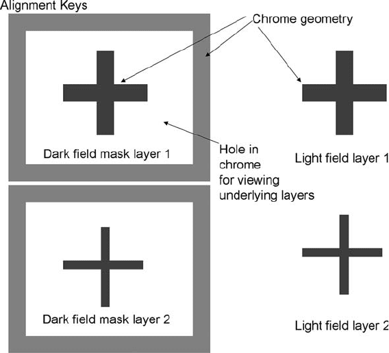
dark field keys are shown as crosses. This author likes to use
crosses about 100 mm long and 20 mmwideforthefirstlayer
for contact printing. The layer to be aligned to it has a cross
98 mm long and 18 mm wide, giving a tolerance of about –
1 mm. Thus, a smaller cross fits on top of a larger cross that is
etched into the wafer. Recall that the mask design dimensions
and the geometry dimensions on the first layer will vary based
on the process biases introduced, so those biases need to be
understood before laying out the align keys. Most often all
layers are aligned to the first layer, so the first layer needs keys
for each layer to be aligned to it. Align keys must be posi-
tioned on the mask and die so that the microscopes on the
align tool can easily locate them.
A very common mistake in mask layout occurs in dark field
masks. Trying to find align keys using a microscope on top of a
dark field mask can be very difficult. Since most of the mask is
chrome, the underlying layer can only be seen through the align
key itself. Draw a large box of clear geometry and put a small
chrome align key inside the clear box. The large box makes it
easy to find the align key and makes it much easier to find the
align key on the underlying layer (Fig. 1.5).
Fig. 1.5. Alignment keys for dark- and light-field masks. On the left, align keys in a dark
field mask must be surrounded with a large clear area to make it possible to see the
geometry underneath that a layer is being aligned to.
Microfabrication Techniques for Biologists 11
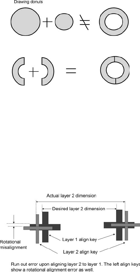
Another common mistake is to draw closed shapes by putting
one square or circle on top of another (Fig. 1.6). Human eyes can
see the resulting donut, but a computer generating a mask sees two
circles on top of each other and writes both. What was supposed to
be a donut or outline becomes a solid shape. Therefore, closed
shapes must be drawn as two parts, as seen in Fig. 1.6.
Besides the tolerances of specific geometries, another impor-
tant tolerance indicates how each layer lines up to the previous
layer. Masks and wafers can have run-in and run-out errors. These
are where a design may call for a dimension across an entire wafer,
say 100.000 mm, but the actual dimension is, for example,
100.005 mm. The layer placed on top of that layer may be
99.009 mm, giving a 0.006 mm or 6 m m run-out error. Such
errors can be introduced at the mask shop by bowing of substrates
and masks in the align tool and by thermal mismatch (Fig. 1.7).
Fig. 1.6. Drawing closed shapes. A computer recognizes only solid shapes and cannot
subtract one pattern from another.
Fig. 1.7. Alignment and runout errors seen upon alignment of the top layer (light gray
crosses) to the layer etched into the wafer (dark crosses).
12 Chinn
Taking handedness or chirality into account is important when
designing a photomask. Masks are usually used chrome side down
or viewed through the back of the mask relative to the design
artwork. One can buy boxes of unexposed photomasks covered
with chrome and photoresist, quite useful in the typical laboratory.
Do not open them except in yellow lights. By placing an existing
mask in contact with a blank mask, a copy can be made. Typically
some pattern fidelity is lost, and the copied mask is a left-hand
version of the original. Copying a mask a second time restores the
chirality to its original. To reverse a mask, i.e., to use it with
negative photoresist, for example, one can make a copy, strip the
resist, sputter or evaporate a different metal onto it (such as tita-
nium), etch the chrome in a chrome specific etchant, and have a
titanium reversal copy. Edges may be somewhat rougher than the
original.
Sometimes test patterns that can define resolution, or measure
overlay alignment (such as a vernier pattern), are added to the
photomask. Many chip designers have various test patterns avail-
able to cut and paste into designs. Electrical devices often have
special test devices such as resistors or individual transistors built
into a device in the test pattern section of the chip.
If multiple devices, or dies, are on a single wafer, it is usually
diced up as a final processing step. The blades used in dicing saws
are as thin as 200 mm, but by leaving a scribe line between dies of at
least 500 mm makes the dicing operation much easier.
Packaging is often the most expensive part of an IC and is
often overlooked during the device design stage. Final packaging
can be a very difficult part of building a device. In ICs, only
electrons go in, and only electrons and heat leave the chip. In
micromachines, electrons, heat, fluids, mechanical energy,
photons, and perhaps even magnetic energy all may go in and
out; consequently, the package can be very complex and probably
cannot be purchased off the shelf. It is difficult to get information
from a micro level to the human who will make decisions based on
what happens at the micro level. Thus the designer of microma-
chines must take the package into account early in the design
process.
Consider when designing a mask how the finished device will
be contacted electrically. Electrical input and output to the outside
world is usually done with bond pads. Bond pads are squares of
metal that are the terminus of electrical wires patterned on the
chip. Special micromanipulators are available to put tiny probes
onto bond pads, but if space allows, bond pads 2 mm on a side can
be contacted with the crudest probe tips. We recommend making
them as large as space permits.
Another type of mask is a shadow mask.Thisisusuallyathin
sheet of metal with holes cut in it. The shadow mask is placed in
contact with the substrate and put into an evaporator or sputterer
Microfabrication Techniques for Biologists 13