Gupta D. (Ed.). Diffusion Processes in Advanced Technological Materials
Подождите немного. Документ загружается.


curvature of the resistance change curves shown in Fig. 9.7. Consequently,
we would expect the void growth rate for high current density test cases
not to be linearly proportional to the current density, which is in contrast
to Eq. (1). We can, of course, make the liner joule heating less of a factor
by increasing the liner thickness at the expense of the line conductivity.
9.7 Fast Diffusion Paths
9.7.1 Free Surface and Grain Boundary Diffusion
Asurprisingly wide range of activation energies, from 0.5 to 2 eV, for
electromigration in thin-film Cu lines has been reported,
[76–78, 87–97]
and
many diffusion mechanisms (bulk, grain boundary, surface, and interface)
have been proposed to explain these results. It is important to identify the
dominant diffusion paths in Cu lines. Once the fast diffusion path is iden-
tified, we may find a way to reduce the fast diffusivity therein and
increase the Cu reliability. This section discusses the electromigration
studies of liftoff, unpassivated Cu lines of widths varying from 0.15 mm
(bamboo) to 10 mm (polycrystalline), to differentiate the relative contri-
butions of surface from grain boundary transport.
[80]
The test structure
[98]
consisted of Cu lines connected to two sputtered
Ti (10 nm)W (200 nm) bar electrodes, the purpose of which was to sim-
ulate blocking contacts and to measure the drift velocity of Cu in the
tested lines. The Ti (10 nm)Ta (15 nm)Cu (300 nm) test lines were all
deposited by e-gun evaporation at a base pressure of 10
7
torr and fabri-
cated by a liftoff process using e-beam lithography.
[98]
The bottom Ti layer
in the TiW bar served as an adhesion layer to SiO
2
and in the TiTaCu
line was used to reduce the contact resistance between Ta and W. The Ta
film was a diffusion barrier layer between Ti and Cu. The Cu test lines
were 0.15 to 10 mm wide and overlapped the TiW bar by 0.85 and 1.0
mm for 0.15- to 0.25-mm-wide lines and 0.75- to 10-mm-wide lines,
respectively. The samples were annealed in helium at 400°C for 3 hours
before testing to stabilize the microstructure. Bamboo-like, near-bamboo,
and polycrystalline structures were found in the metal linewidths between
0.15 to 0.5 mm, 0.75 to 1 mm, and 2 to 10 mm, respectively. The samples
were tested in a vacuum furnace at temperatures ranging from 255 to
405°C with a current density of 15 mA/mm
2
in a chamber pressure of 15
torr of nitrogen. Mass transport of Cu in the Cu lines as a function of tem-
perature was measured using both drift-velocity (void growth rate) and
resistance measurements. Void size was measured by scanning electron
microscopy. For these test structures, complete blocking boundaries exist
at both ends of the line. Edge displacement void growth, ∆L, at the cathode
422 DIFFUSION PROCESSES IN ADVANCED TECHNOLOGICAL MATERIALS
Chapter-09 11/29/04 6:50 PM Page 422

ELECTROMIGRATION IN CU THIN FILMS, HUETAL. 423
end exposed the Ti/Ta underlayer and caused the conductor line resistance
to increase by∆R. The drift velocity of Cu was directly related to the rate
of edge displacement by Eq. (11b) as v
d
∆L∆t and can be estimated by
v
d
∆L
f
t, assuming a constant drift velocity, where t is the amount of
time required to grow a void to critical size ∆L
f
. (Incubation times were
considered negligible.)
Let us assume the Cu/Ta interface diffusion is significantly slower
than GB and surface diffusion. The evidence of the slow Cu/Ta diffusion
is given in Sec. 9.7.3. For the case of a bamboo-like grain structure, the
contribution of mass transport by electromigration along GBs is negligi-
ble because there is no continuous GB path and the electromigration driv-
ing force is perpendicular to the GBs. The surfaces at the sidewalls and on
top of the lines become the fast diffusion paths in liftoff structures. The
combination of Eqs. (1) and (3) can be written as:
v
d
d
S
(2w 1h)D
S
Z
*
S
erj(kT). (12a)
Equation (12a) states that the marker velocity (or void growth rate) in the
bamboo-like line structure will be increased as the metal linewidth or
thickness is decreased, at a fixed sample temperature and current density.
For the case of a polycrystalline line structure, the effective drift
velocity becomes:
v
d
{(d
GB
d)(1 dw)D
0
GB
exp(Q
GB
kT)Z
*
GB
d
S
(2w 1h)D
0
S
exp(Q
S
kT)Z
*
S
}erjkT, (12b)
where D
0
GB
and D
0
S
are the pre-exponential factors, and Q
GB
and Q
S
are the
activation energies for grain boundary and surface diffusion, respectively.
In this case, we would expect the drift velocity to be less sensitive to
linewidth for large w, because (1 dw) 1.
Surface and grain boundary diffusivities are known to be dependent
on purity, the orientation of the surface, and the plane of the grain bound-
aries;
[75, 79, 84, 99]
however, the measured values were generally average val-
ues obtained by sampling drift velocities along many fast paths. For
example, the number of grain surfaces sampled in a 0.25-mm-wide line for
a void size of 1 mm is estimated to be more than 300, using ∆Lhw(d
S
d
(2h w)), where ∆L 1 mm, w 0.25 mm, h 0.3 mm, d
S
0.5 nm,
and d 0.8 mm.
The size of the void ∆L
f
at the cathode end of the line (mass depletion)
was measured from SEM micrographs. Hillock growth at the anode end
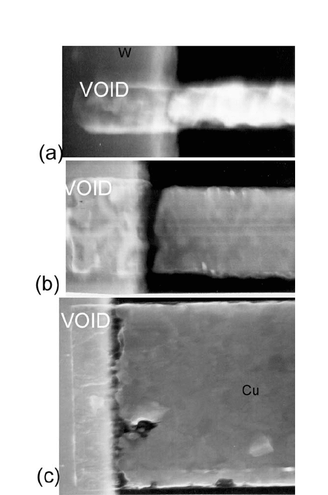
of the line was also observed. Figure 9.9(a) to (c) shows the SEM micro-
graphs of Cu depletion at the cathode ends of 0.15-, 1-, and 5-mm-wide lines
for t 6.8, 30, and 18 hours, respectively, with j 15 mAmm
2
at 314°C.
Chapter-09 11/29/04 6:50 PM Page 423
424 DIFFUSION PROCESSES IN ADVANCED TECHNOLOGICAL MATERIALS
Figure 9.9 SEM microgaphs of tested Cu lines with j 15 mA/mm
2
at 314
o
C for
various linewidths. (a) 0.15-mm-wide line for t 6.8 hours; (b) 1-mm-wide line for
t 30 hours; (c) 5-mm-wide line for t 18 hours.
Chapter-09 11/29/04 6:50 PM Page 424
ELECTROMIGRATION IN CU THIN FILMS, HUETAL. 425
The Cu drift velocity was estimated by ∆Lt, where ∆L and
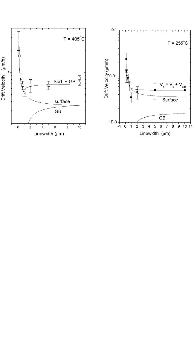
t are the mean void size and mean lifetime, respectively. Figure 9.10
shows the drift velocity v
d
as a function of w. A careful inspection of
Fig. 9.10 shows that the velocity decreases monotonically with linewidth
w but goes through a minimum at w 1 mm and then increases to a con-
stant value. The lines are the least-squares fits of the data to Eq. (12a) for
w 1 mm and to Eq. (12b) for w 1 mm, respectively. In the case of the
bamboo grain structures for w 1 mm, grain boundary transport is elim-
inated and only surface diffusion of the Cu lines is considered. The film
thickness, the profiles of the cross-sectional area (trapezoid shape) of the
line, and the values of erjkT are known. The only adjustable parameters
in Eq. (12a) are d and d
S
D
S
Z
*
S
. The best values of fitting parameters for the
data w 1 mm were used as the constrained values for analyzing the data
points for w 1 mm in Eq. (12b). The solid lines shown in Fig. 9.10 are
the least-squares fits. The contribution of Cu drift velocity in grain bound-
aries is also pointed out in Fig. 9.10. The ratio of v
S
to v
GB
for a 10-mm-
wide line decreases from 2 to 1 as T increases from 255 to 405°C. This
indicates that major void growth is due to surface migration even in a
polycrystalline 10-mm-wide line for T 250°C. The activation energy of
grain boundary diffusion is 0.2 eV higher than that of surface diffusion,
and the ratio of (d
S
D
0
S
Z
*
S
)(d
GB
D
0
GB
Z
*
GB
) is about 0.02. The extracted values
of fitting parameters from the data in Fig. 9.10, d
GB
D
GB
Z
*
GB
erj and
d
S
D
S
Z
*
S
erj, as a function of 1T are plotted in Fig. 9.11. The activation
Figure 9.10 Plot of drift velocity as a function of linewidth stressed at sample tem-
peratures of (a) 405 and (b) 255
o
C. The lines are least-squares fits.
Chapter-09 11/29/04 6:50 PM Page 425
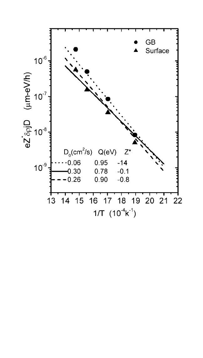
energies of surface and grain boundary diffusion are 0.9 and 1.1 eV,
respectively. The derived values of activation energies are in good agree-
ment with the reported values of 0.78 to 0.90 eV for the activation energy
of surface diffusion
[75, 99]
and 0.88 to 0.95 eV for grain boundary diffu-
sion.
[81–83]
The apparent effective charge number Z
*
can be estimated by
using the diffusivities and data in Fig. 9.11. From the above relationship,
after substituting the surface diffusivities
[79, 99]
computed either from D
0
S
0.15 cm
2
s and Q
S
0.78 eV, or D
0
S
0.26 cm
2
s and Q
S
0.90 eV, at
400°C, r 5.0 mΩ-cm, and d
S
0.5 nm, we obtain Z
*
S
0.1 or 0.8,
respectively. The negative sign in Z
*
means that Cu atoms drifted in the
direction of the electron wind force. Using the grain boundary diffusivi-
ties,
[83]
we obtain Z
*
GB
14. The values of Z
*
estimated in this way
426 DIFFUSION PROCESSES IN ADVANCED TECHNOLOGICAL MATERIALS
Figure 9.11 Plot of d
S
D
S
Z
*
S
E
S
and d
GB
D
GB
Z
*
GB
E
GB
vs. 1/T.The straight lines are cal-
culated from the best-fitting values of Z
*
to the data using the known values of
d
S
D
S
E
S
and d
GB
D
GB
E
GB
.
Chapter-09 11/29/04 6:50 PM Page 426

ELECTROMIGRATION IN CU THIN FILMS, HUETAL. 427
depend on the accuracy of published values of D
0
and Q. Although the
absolute value of Z
*
S
Z
*
GB
appears to be consistent with a theoretical pre-
diction, the electron wind force decreases as an atom moves from the bulk
to a grain boundary and to a surface.
[100]
In summary, a systematic study of Cu electromigration drift velocity
shows that the paths for fast migration are the surfaces in bamboo-like and
near-bamboo structures, and a mixture of surface and grain boundaries in
polycrystalline films. The activation energy for grain boundary diffusion
is approximately 0.2 eV higher than that of surface diffusion, and the ratio
of (d
S
D
0
S
Z
*
S
E
S
)(d
GB
D
0
GB
Z
*
GB
E
GB
) is approximately 0.02.
9.7.2 Ambient Effect
The effect of impurity on Cu surface diffusion has been reported.
[75, 79, 101, 102]
The measured surface diffusivities are strongly dependent on the atmos-
phere and absorbed impurity on the surface of the diffusion experiments.
The Cu surface self-diffusion increases with the vapors of solute Pb, Tl,
Bi, or Cl over the Cu surface
[75, 79]
and is reduced with the absorption of C,
Ca, Mn, or O
2
on the Cu surface.
[79, 101]
The kink and ledge sites of the Cu
surface can absorb impurities that reduce the concentration of diffusing
defects and thus suppress the rate of surface self-diffusion.
[75]
The Cu sur-
face diffusivity is higher in an oxygen atmosphere or vacuum than in a
hydrogen atmosphere.
[75, 79]
This result suggests that oxygen may remove
the inhibiting effect of surface impurities.
[75]
To this end, the electromi-
gration lifetime of unpassivated 0.18-mm-wide bamboo-like Cu lines with a
Fig. 9.3(e) structure was measured. The samples were tested in a vacuum
furnace with a chamber pressure of 10 to 30 torr of high-purity nitrogen
or forming gas (N
2
5% H
2
) in the temperature range 180 to 362°C. The
total impurity concentration in the nitrogen gas was less than 1 ppm, with
H
2
O the major impurity at 0.5 ppm. The concentration of oxygen was
found to be less than 10
7
ppm from an oxygen detector. With a test struc-
ture shown in Fig. 9.3(e), the Cu void growth rate at the cathode end of
the line was the same as the Cu drift velocity because the end of the M1
line was connected to a completely blocking boundary of W M0. The
migration fast path is the top surface in the bamboo-like damascene line.
Thus the extracted activation energy from these samples is the electromi-
gration activation energy of Cu surface diffusion. The mean lifetime t
as a function of 1/T is plotted in Fig. 9.12. The electromigration activation
energies of Cu surface diffusion in nitrogen and forming gas are found to be
0.7 ± 0.1 and 0.9 ± 0.1 eV, respectively. The derived values of electromi-
gration activation energies are in good agreement with the reported values
of the activation energy of surface diffusion of 0.78 and 0.95 eV measured
Chapter-09 11/29/04 6:50 PM Page 427
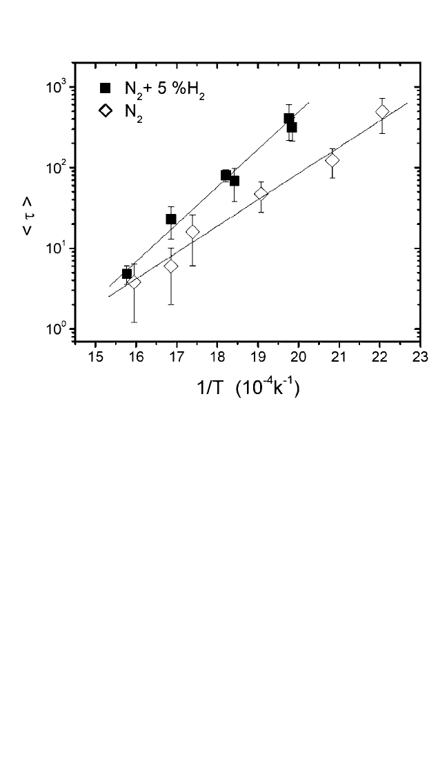
in oxygen (10
5
torr) and hydrogen (760 torr) ambients, respectively.
[75, 79]
Higher values reflect the slowing of surface diffusion by the presence of
gases compared to the value of 0.5 eV measured in situ in ultrahigh vac-
uum on a clean Cu surface.
[103]
9.7.3 Alloying Effect
This section discusses the results of electromigration in pure Cu and
Cu alloys using standard drift velocity test structures [Fig. 9.3(a)]. The
tested samples were the Ta/Cu or Cu alloys/Ta line segments on top of a
W underlayer line. The Cu line segments were patterned by an ion milling
technique.
[28]
The top and bottom Ta layers served as an etch mask and
etch stop. The bottom Ta layer was removed by RIE using CF
4
chemistry.
During RIE processing, CuF
x
may have formed on the surfaces of two
sidewalls of the Cu lines. All the samples were annealed in He at 400°C
for 3 hours. The final metal structure is Ta (20 nm)/Cu or Cu alloys
(300 nm)Ta (20 nm). The top Ta layer thickness was estimated from
428 DIFFUSION PROCESSES IN ADVANCED TECHNOLOGICAL MATERIALS
Figure 9.12 Plot of mean lifetime t vs. 1/T. The straight lines are least-squares
fits.The data points are obtained from the samples using a Fig.9.3(e) test structure.
Chapter-09 11/29/04 6:50 PM Page 428
ELECTROMIGRATION IN CU THIN FILMS, HUETAL. 429
Augh electron spectroscope (AES) analysis with Ar
sputtering profiles.
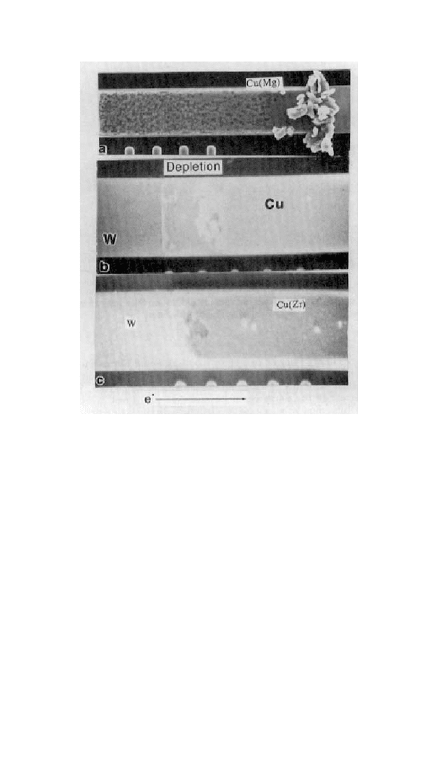
The SEM micrographs in Figure 9.13 show the depleted cathode ends
after electromigration stressing of 5-mm-wide lines at 250°C for 55 hours
of a TaCu(Mg)Ta structure, and for 128 hours of a Ta/pure Cu/Ta struc-
ture and a Ta/Cu(Zr)/Ta structure. Voids developed under the top, immo-
bile Ta layer and along the sidewalls of the line in this sandwich structure.
The dominant Cu electromigration paths would be along the Cu grain
boundary plane and/or along the two Cu sidewalls. These Ta layers are not
seen in Fig. 9.13 because of the high penetration depth of the 30 KeV elec-
tron beam in the SEM. Many fine islands are seen in the depleted Cu(Mg)
sample. The edge displacement ∆L of TaCu(1 wt.% Mg), pure Cu, and
Cu(0.7 wt.% Zr)Ta isolated lines as a function of stress time is plotted in
Fig. 9.14.
[104]
The linear behavior of Cu(Mg) and pure Cu indicates that
drift velocities of Cu in Cu(Mg) and pure Cu are independent of time, with
little incubation time for a sample temperature of 250°C. In the case of
Cu(Zr), a nonlinear behavior was observed. The combination of a small
Figure 9.13 SEM micrographs of 5-mm-wide lines after electromigration stressing
with 2 10
6
A/cm
2
at 250°C for (a) 55 hours with Cu(Mg); (b) and (c) 128 hours
with pure Cu and Cu(Zr), respectively.
Chapter-09 11/29/04 6:50 PM Page 429
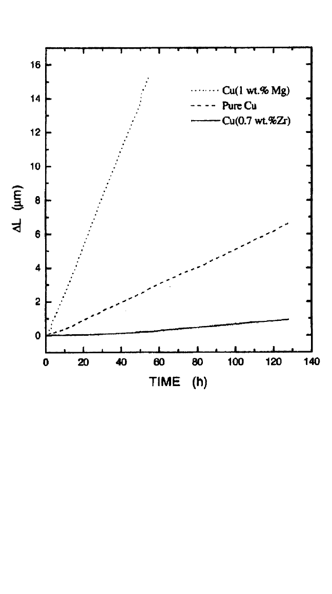
Cu grain size in Cu(Mg), the formation of fine Cu islands seen in Fig.
9.13, and the lack of a pinning effect of Cu by Mg along the fast diffusion
paths resulted in enhancing the Cu line damage. The void growth rate on
the Cu line in Cu(Mg) was found to be 5 and 35 times faster than in pure
Cu and Cu(Zr), respectively. This is partly due to the fine islands left
behind the depletion front. The islands can be formed if Cu on the trailing
surface of the grains has not been completely fed into grain boundary
depletion before the voids encircle the grain.
The activation energy for electromigration in pure multigrained Cu is
found to be 0.77 ± 0.04 eV, which is less than the Cu grain boundary
diffusion.
[80, 82]
The value of 0.77 eV should represent the surface diffusion
activation energy along the two sidewalls of the line.
430 DIFFUSION PROCESSES IN ADVANCED TECHNOLOGICAL MATERIALS
Figure 9.14 Edge displacement in Cu and various Cu alloys as a function of stress
time at 250°C.
Chapter-09 11/29/04 6:50 PM Page 430
ELECTROMIGRATION IN CU THIN FILMS, HUETAL. 431
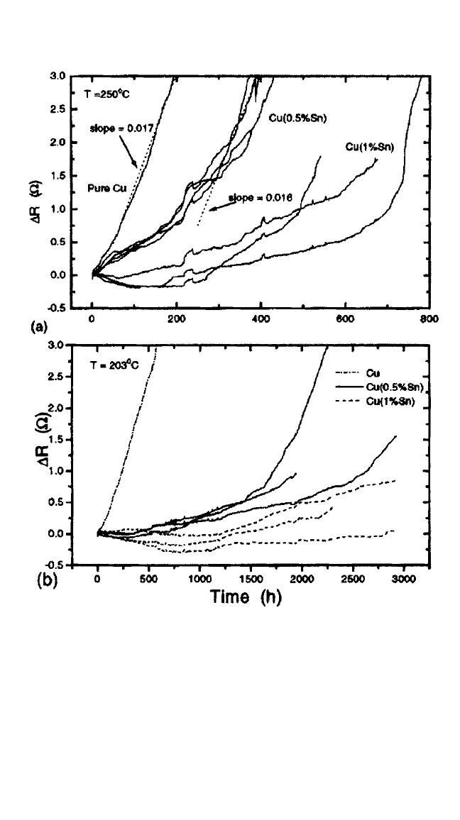
The time for an equivalent resistance change ∆R corresponding to
electromigration damage in pure Cu and Cu(Sn) alloys is progressively
increased as a function of Sn content in the Cu at 250 and 203°C for
2.0-mm-wide, 0.3-mm-thick lines, as shown in Fig. 9.15(a) and (b), respec-
tively. A deviation from linear behavior was observed in Cu(Sn). This
nonlinear behavior of the line resistance change is similar to that observed
during electromigration in Al(Cu),
[105]
in which Cu depletion precedes
Figure 9.15 Line resistance change vs. electromigration stressed time for Cu and
Cu(Sn) alloys with j 2.6 10
6
A/cm
2
at temperatures of (a) 250 and (b) 203°C.
Chapter-09 11/29/04 6:50 PM Page 431