Guozhong Cao. Nanostructures & Nanomaterials: Synthesis, Properties & Applications
Подождите немного. Документ загружается.


3
96
Nanostructures and Nanomaterials
9.4.
Biological Applications of Nanoparticles
Biological applications of colloidal nanocrystals have been summarized in
an excellent review article, and the following text is mainly based on this
article.63 One important branch
of
nanotechnology is nanobiotechnology.
Nanobiotechnology includes (i) the use
of
nanostructures as highly
sophisticated scopes, machines or materials in biology andor medicine,
and (ii) the use of biological molecules to assemble nanoscale
structure^.^^
The following will briefly describe one of the important biological appli-
cations
of
colloidal nanocrystals: molecular recognition. But there are
many more biological applications of nanotechnology. 64-6
Molecular recognition is one
of
the most fascinating capabilities of
many biological molecules.67@ Some biological molecules can recognize
and bind to other molecules with extremely high selectivity and speci-
ficity. For molecular recognition applications, antibodies and oligonu-
cleotides are widely used as receptors. Antibodies are protein molecules
created by the immune systems of higher organisms that can recognize a
virus as a hostile intruder or antigen, and bind to it in such a way that the
virus can be destroyed by other parts of the immune system.67
Oligonucleotides, known as single stranded deoxyribonucleic acid
(DNA), are linear chains
of
nucleotides, each of which is composed
of
a
sugar backbone and a base. There are four different bases: adenine
(A),
cytosine
(C),
guanine
(G),
and thymine (T).67 The molecular recognition
ability of oligonucleotides arises from two characteristics. One is that each
oligonucleotide is characterized by the sequence
of
its bases, and another
is that base A only binds to T and
C
only to
G.
That makes the binding of
oligonucleotides highly selective and specific.
Antibodies and oligonucleotides are typically attached to the surface
of
nanocrystals via (i) thiol-gold bonds to gold nanoparti~les,~~,~~ (ii) covalent
linkage to silanized nanocrystals with bifknctional crosslinker mole-
cule~:’-~~ and (iii) a biotin-avidin linkage, where avidin is adsorbed on the
particle ~urface.~~.~~ When a nanocrystal is attached or conjugated to a
receptor molecules,
it
is “tagged”. Nanocrystals conjugated with a receptor
can now be “directed” to bind to positions where ligand molecules are pres-
ent, which “fit” the molecular recognition of the receptor76 as schematically
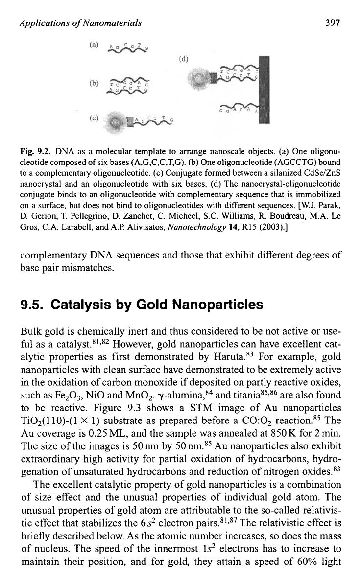
shown in Fig.
9.2.
This facilitates a set of applications including molecular
For example, when gold nanoparticles aggregate, a change
of
coior from ruby-red to blue is observed, and this phenomenon has been
exploited for the development of very sensitive colorimetric methods
of
DNA analysis.80 Such devices are capable
of
detecting trace amounts of a
particular oligonucleotide sequence and distinguishing between perfectly
Applications
of
Nanomaterials
397
Fig.
9.2.
DNA
as a molecular template to arrange nanoscale objects. (a) One oligonu-
cleotide composed of six bases (A,G,C,C,T,G).
(b)
One oligonucleotide (AGCCTG) bound
to a complementary oligonucleotide. (c) Conjugate formed between a silanized CdSe/ZnS
nanocrystal and an oligonucleotide with six bases. (d) The
nanocrystal-oligonucleotide
conjugate binds to an oligonucleotide with complementary sequence that is immobilized
on a surface, but does not bind to oligonucleotides with different sequences. [W.J. Parak,
D.
Gerion, T. Pellegrino,
D.
Zanchet, C. Micheel, S.C. Williams,
R.
Boudreau, M.A. Le
Gros,
C.A.
Larabell, and
A.P.
Alivisatos,
Nanotechnology
14,
R15
(2003).]
complementary DNA sequences and those that exhibit different degrees of
base pair mismatches.
9.5.
Catalysis by
Gold
Nanoparticles
Bulk gold is chemically inert and thus considered to be not active or use-
ful as a catalyst.8',s2 However, gold nanoparticles can have excellent cat-
alytic properties as first demonstrated by Har~ta.~~ For example, gold
nanoparticles with clean surface have demonstrated to be extremely active
in the oxidation of carbon monoxide if deposited on partly reactive oxides,
such as Fe203, NiO and MnO,. y-al~mina,~~ and are also found
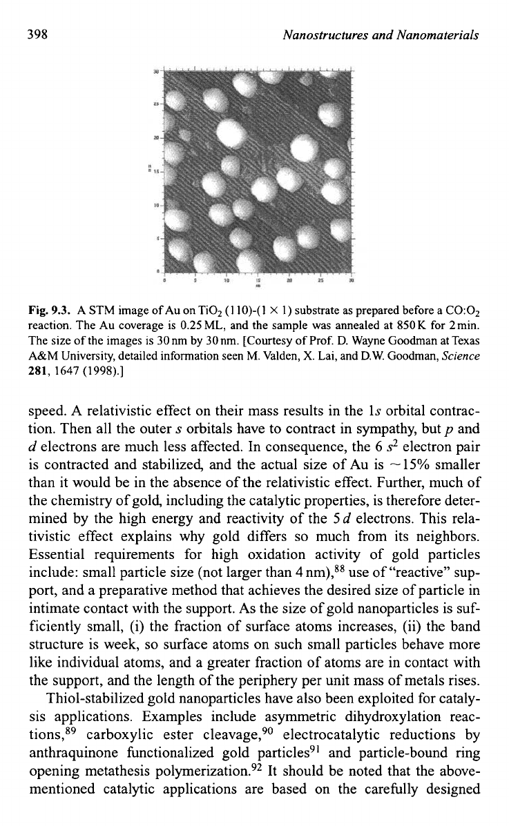
to be reactive. Figure
9.3
shows a STM image of Au nanoparticles
Ti02(
1
lo)-(
1
X
1)
substrate as prepared before a
CO:O2
reaction.85 The
Au coverage is
0.25
ML, and the sample was annealed at
850
K
for
2
min.
The size of the images is
50
nm by
50
nm.85 Au nanoparticles also exhibit
extraordinary high activity for partial oxidation of hydrocarbons, hydro-
genation of unsaturated hydrocarbons and reduction of nitrogen oxides.83
The excellent catalytic property of gold nanoparticles is a combination
of size effect and the unusual properties of individual gold atom. The
unusual properties of gold atom are attributable to the so-called relativis-
tic effect that stabilizes the
6
s2
electron
pair^.^',^^
The relativistic effect is
briefly described below. As the atomic number increases,
so
does the mass
of nucleus. The speed of the innermost
ls2
electrons has to increase to
maintain their position, and for gold, they attain a speed of
60%
light
398
Nanostructures and Nanomaterials
Fig.
9.3.
A STM image of Au
on
Ti02
(1
lo)-(
1
X
1)
substrate as prepared before a
CO:O2
reaction. The Au coverage is
0.25
ML, and the sample was annealed at
850
K
for
2
min.
The size of the images is 30 nm by 30nm. [Courtesy of Prof.
D.
Wayne Goodman at Texas
A&M University, detailed information seen M. Valden,
X.
Lai, and D.W. Goodman,
Science
281,
1647
(1998).]
speed.
A
relativistic effect on their mass results in the
1s
orbital contrac-
tion. Then all the outer
s
orbitals have to contract in sympathy, but
p
and
d
electrons are much less affected. In consequence, the
6
s2
electron pair
is contracted and stabilized, and the actual size of
Au
is
-
15%
smaller
than it would be in the absence of the relativistic effect. Further, much of
the chemistry of gold, including the catalytic properties, is therefore deter-
mined by the high energy and reactivity of the
5d
electrons. This rela-
tivistic effect explains why gold differs
so
much from its neighbors.
Essential requirements for high oxidation activity of gold particles
include: small particle size (not larger than
4
nm),ss use of “reactive” sup-
port, and a preparative method that achieves the desired size of particle in
intimate contact with the support.
As
the size of gold nanoparticles is suf-
ficiently small, (i) the fraction of surface atoms increases, (ii) the band
structure is week,
so
surface atoms on such small particles behave more
like individual atoms, and a greater fraction of atoms are in contact with
the support, and the length of the periphery per unit mass of metals rises.
Thiol-stabilized gold nanoparticles have also been exploited
for
cataly-
sis applications. Examples include asymmetric dihydroxylation reac-
tion~,~~ carboxylic ester cleavage,90 electrocatalytic reductions by
anthraquinone hnctionalized gold particles9’ and particle-bound ring
opening metathesis p~lymerization.~~ It should be noted that the above-
mentioned catalytic applications are based on the carefully designed

Applications
of
Nanomaterials
399
chemical functionality of the ligand shell, instead of the potential catalytic
activity of a nanostructured clean metal surface.
9.6.
Band
Gap
Engineered Quantum Devices
Band gap engineering
is
a general term referring to the synthetic tailoring
of
band gaps93.94 with the intent to create unusual electronic transport and
optical effects, and novel devices. Obviously, most of the devices based on
semiconductor nanostructures are band gap engineered quantum devices.
However, the examples discussed in this section are focused mainly on the
device design and fabrication of quantum well and quantum
dot lasers by
vapor deposition and lithography techniques.
9.6.1.
Quantum
well devices
Lasers fabricated using single or multiple quantum wells based on
111-V
semiconductors as the active region have been extensively studied over the
last
two
decades. Quantum well lasers offer improved performance with
lower threshold current and lower spectra width as compared to that of
regular double heterostructure lasers. Quantum wells allow the possibility
of independently varying barriers and cladding layer compositions and
widths, and thus separate determination of optical confinement and
BARRIER
r
rACTlVE
CONDUCTION
CONDUCTION&LADDING
BAND
BAND
'-up
VALENCE
BAND
VALENCE
n
BAND
SINGLE OUANTUM MULTIOUANTUM WELL
WELL
BARRIER
GRADED REGION
BAND BAND
CONDUCTION
CONDUCT
ION&
I
I
VALENCE
A-
VALENCE
BAND BAND
GRADED INDEX
SINGLE QUANTUM
WELL
MOD
I
FI
ED MULTIQUANTUM
WELL
Fig.
9.4.
Schematic energy band diagrams
of
different
types
of
quantum
well
structures
used to optimize
the
laser performance.
[PK.
Bhattacharya and N.K. Dutta,
Ann.
Rev.
Muter:
Sci.
23,
79
(1993).]

400
Nanostructures and Nanomaterials
electrical injection. Quantum well lasers were first fabricated using the
GaAslAlGaAs material ~ystems?~.~~ and Fig.
9.4 shows schematic energy
band diagrams of different types of quantum well structures used to opti-
mize the laser perf~rrnance.~~ One of the main differences between the
single quantum well and the multiple quantum well lasers is that the con-
finement factor of the optical mode is significantly smaller for the former.
This results in higher threshold carrier and current densities for single
quantum well lasers; however the confinement factor of single quantum
well lasers can be significantly increased using a graded-index cladding
structure.98 InGaAsP/InP is another material system used in the fabrica-
tion of quantum well
laser^.^^.'^
InGaAsN/GaAs quantum wells are yet
another exarnple.l0' Strain has been explored and introduced into quantum
well lasers, since strain can alter the band structure parameters signifi-
cantly to produce many desirable features such as better high temperature
performance resulting from reduced Auger recombination, small chirp,
and high bandwidth.97 Other quantum well optical devices have also been
extensively studied and include quantum well electroabsorption and elec-
tro-optic modulators, quantum well infrared photodetectors, avalanche
photodiodes and optical switching and logic devices.
Blue/green light-emitting diodes
(LED)
have been developed based on
nanostructures of wide-band gap II-VI semiconductor rnaterials.lo2 Such
devices take direct advantages
of quantum well heterostructure configura-
tions and direct energy band gap to achieve high internal radiative effi-
ciency. Various
LED
at short visible wavelengths have been fabricated
based on nanostructures or quantum well structures of ZnSe-based mate-
rial~*~~,'@' and ZnTe-based materials.Io5
Blue/green lasers were first demon~trated'~~~'~~ in a pn injection diode
that employed a configuration sketched in Fig.
9.5.'02
In this structure, the
Zn(S,Se) ternary layers were introduced to serve as cladding layers for the
optical waveguide region with the ZnSe layers and thus provide the elec-
tronic barriers for the (Zn,Cd)Se quantum wells. A lot of effects have been
devoted to the improvement of materials and structure-design from the
above struct~re.'~*,~~~ The typical blue/green lasers operate continuously
at room temperature and emit a significant amount of power with wave-
lengths ranging from
463
to 514nm depending on the actual structure.
The various laser structures are composed of (Zn,Mg)(Se,S) and Zn(Se,S)
cladding layers with (Zn,Cd)Se quantum wells and possess a graded
ohmic contact consisting of Au metal on a pseudo-alloy of Zn(Se,Te).
Heterojunction bipolar transistor (HBT) is an example of nanostruc-
tured devices based
on
GeSi/Si nanostructures."03'1
'
For this structure,
the GeSi layer is thick enough
so
that no quantum confinement occurs. In
Applications
of
Nanomaterials
40
1
Fig.
9.5.
Schematic diagrams
of
key blue/green laser diode configurations and their evo-
lution from the initial laser design to the later laser design.
[L.A.
Kolodziejski,
R.L.
Gunshor, and A.V Nurmikko,
Ann.
Rev.
Muter:
Sci.
25,
71
1
(1995).]
the operation of a bipolar transistor, by applying a small current to the
base, a large amount of current can flow from the emitter to the collector
if the gain is high. Comparing to the conventional bipolar junction tran-
sistor, the HBT offers an advantage
of
reduction of hole injection into the
emitter, due to the valence band discontinuity. The barrier to the hole
injection is exponentially sensitive to the valence band offset,
AE,.
9.6.2.
Quantum dot devices
The key parameter that controls the wavelength is the size of the dot.
Large sized dots emit at longer wavelengths than small sized ones.
Quantum dot heterostructures are commonly synthesized by molecular
beam epitaxy at the initial stages of strained heteroepitaxial growth via the
layer-island or Stranski-Krastanov growth mode.
12a1
l3
Quantum dots have been established their use in lasers and detectors.
Quantum dot lasers with ultralow-threshhold current densities and low
sensitivity to temperature variations have been demonstrated."4,'15
Intersublevel detectors made
of
quantum dot nanostructures were found
402
Nanostructures and Nanomaterials
not sensitive to normal-incidence light.116 For the lasers using the quantum
dot media often suffer from insufficient gain for the device to operate at
the ground state wavelength, due to the combined consequence of the low
density of states and the low area density of dots that is normally used.
Several techniques have been developed to overcome this barrier. For
example, several layers of quantum dots are used to increase the modal
gain. Other methods include coating the laser facets to increase their
reflectivity and lengthen the laser cavity.
The efficiency of luminescence from quantum dot structures depends
on a number of factors including the capture of the carriers within the
dots, the minimization of nonradiative recombination channels within
the dots and in the surrounding matrix, and the elimination of defects at
the hetero-interfaces. Embedding quantum dots inside an appropriate
quantum well structure (also referred to as active region) demonstrated
dramatically enhanced emission efficiency and low threshold current, due
to the improved structural and optical properties of the embedding layers,
and the enhanced ability of capturing and confining carriers to the vicin-
ity
of the dots.117’118 Further structural improvement can be achieved by
sandwiching quantum dots in a compositionally graded quantum well.
l9
When the quantum dots of InAs are inserted at the center of composition-
ally graded In,Gal,As layers, the relative emission efficiency has been
increased by nearly an order of magnitude over the emission of dots inside
a constant composition (In,Ga)As structure.
9.7.
Nanomechanics
In the previous two chapters, we have discussed the applications of
SPM
in the field of imaging surface topography and measurement of local
properties of sample surface (Chapter
8)
and nano manipulation and nano-
lithography in fabrication and processing of nanodevices. In this chapter,
we will briefly introduce another important application
of
SPM,
i.e. nano-
devices derived from
SPM.
Although many devices are being investigated
and more are to be developed in the conceivable future, we will take two
examples to illustrate the possibilities and general approaches, specifi-
cally, nanosensors and nanotwizers.
Lang
et
al.
I2O
made an excellent summary
of
the applications of AFM
cantilever based sensors in their tutorial article. When the surface of a can-
tilever or a tip is functionalized in such a way that a chemically active and
a chemically inactive surface is obtained, chemical or physical processes
on the active cantilever surface can be observed using the temporal

Applications
of
Nanomaterials
403
evolvement of the cantilever’s response. Cantilevers can be used as a
nanomechanical sensor device for detecting chemical interactions
between binding partners on the cantilever surface and in its environment.
Such interactions might
be
produced by electrostatic or intermolecular
forces. At the interface between an active cantilever surface and the sur-
rounding medium, the formation of induced stress, the production of heat
or a change in mass can be detected. In general, detection modes can be
grouped into three strands: static mode, dynamic mode and heat mode as
illustrated in Fig.
9.6.120
In the static mode, the static bending of the cantilever beam due to
external influences and chemicallphysical reactions on one of the can-
tilever’s surfaces is investigated. The asymmetric coating with a reactive
layer on one surface of the cantilever favors preferential adsorption of
molecules on this surface. In most cases, the intermolecular forces in the
adsorbed molecule layer produce a compressive stress, i.e. the cantilever
bends. If the reactive coating is polymer and adsorbing molecules can dif-
fuse, the reactive coating will swell and the cantilever beam will bend.
Similarly, if the cantilever beam emerges into a chemical or biochemical
solution, the asymmetric interaction between the cantilever beam and the
surrounding environment results in bending of the cantilever beam. Many
new concepts and devices have been explored.
~2-l~~
In dynamic mode, the cantilever is driven at its resonance frequency. If
the mass of the oscillating cantilever changes owing to additional mass
Fig.
9.6.
AFM cantilever based sensors with detection modes being grouped into three
strands: static mode, dynamic mode and heat mode.
[H.P.
Lang,
M.
Hegner,
E.
Meyer, and
Ch. Gerber,
Nanotechnology
13,
K29
(2002).]

404
Nanostructures and Nanomaterials
deposited on the cantilever, or if mass is removed from the cantilever, its
resonance frequency changes. Using electronics designed to track the res-
onance frequency of the oscillating cantilever, the mass changes on the
cantilever are derived from shifts of resonance frequency. The cantilever
can be regarded as a tiny microbalance, capable
of
measuring mass
changes of less than
1
In dynamic mode, active coatings should
apply on both surfaces of the cantilever to increase the active surface
where the mass change takes places. Dynamic mode works better in gas
than in liquid, which complicates the exact determination of the resonance
frequency of the cantilever. More examples are available in Ref.
126.
In heat mode, the cantilever is coated asymmetrically, one surface with
a layer having a different thermal expansion coefficient than that
of
the
cantilever itself. When such a cantilever is subjected to a temperature
change, it will bend. Deflections corresponding
to
temperature changes in
the micro-Kelvin range can be easily measured. If the coating is catalyti-
cally active, e.g. a platinum layer facilitates the reaction of hydrogen and
oxygen to form water. In such a case, heat is generated on the active sur-
face and will result in bending of the cantilever. Such a method can also
be used in the study of phase transition and measurement of thermal prop-
erties of a very small amount of material~.'*7?'~~
Although the above discussion has been limited on the single cantilever
nanosensors, the same principle is readily applicable to multiple cantilever
nanosensors. For example, a
SPM
cantilever array consisting of more than
1000
cantilevers have been fabri~ated.'~~
9.8.
Carbon Nanotube Emitters
There have been numerous reports describing studies on carbon nanotubes
as field
emitter^,'^@'^^
since the discovery of carbon nanotubes. Standard
electron emitters are based either on thermionic emission of electrons from
heated filaments with low work hnctions or field emission from sharp tips.
The latter generates monochromatic electron beams; however, ultrahigh
vacuum and high voltages are required. Further, the emission current is
typically limited to several microamperes. Carbon fibers, typically
7
pm in
diameter, have been used as electron emitters; however, they suffer from
poor reproducibility and rapid deterioration of the tip.137 Carbon nanotubes
have high aspect ratios and small tip radius
of
curvature. In addition, their
excellent chemical stability and mechanical strength are advantageous
for application in field emitters. Rinzler
et
demonstrated laser-
irradiation-induced electron field emission from an individual multiwall

Applications
of
Nanomaterials
405
nanotube. Although the emission current of a single tube is constrained
because of its very small dimensions, an array of nanotubes oriented per-
pendicular to an electrode would make an efficient field emitter.
De Heer and co-workers first demonstrated a high-intensity electron
gun based on field emission from an array
of
oriented carbon nano-
tubes.130 Field emission current densities
of
-
0.1 mA/cm2 were observed
when a voltage of 200V was applied, and a current density of
>100mA/cm2 was realized at
700Y The
gun
was reported to be air sta-
ble and inexpensive to fabricate, and hnctions stably and reliably for long
time. However, later research found a gradual degradation with time of the
emission performances on both single-wall carbon nanotube and multi-
wall carbon nanotube emitters.'35 The degradation was explained by the
destruction of nanotubes by ion bombardment with ions either from gas
phase ionization or anode emission. It was also found that the degradation
of single-wall carbon nanotube emitter is significantly faster (a factor
2
lo),
since they are more sensitive to electron or ion bombardment.
A flat panel display based on nanotube field emission was also demon-
~trated.'~~
A
32
X
32
matrix-addressable diode nanotube display prototype
was fabricated and a steady emission was produced in
lop6
torr vacuum.
Pixels were well defined and switchable under a half-voltage "off-pixel''
scheme. A fully sealed field emission display of
4.5
inch in size has been
fabricated using single-wall carbon nanotube-rganic binders.'38 The
nanotubes were vertically aligned using paste squeeze and surface rubbing
techniques, and fabricated displays were fully scalable at temperatures as
low as
4
15°C.
The turn-on field of
1
V/pm and brightness of
1800
cd/m2
at 3.7V/pm was observed on the entire
4.5
inch area from the green
phosphor-indium-tin-oxide glass. Figure
9.7
shows a
CRT
lighting ele-
ment equipped with aligned CNT emitters and the electron tube is
20
mm
in diameter and 75 mm long.'39
A
test
of
this cathode-ray tube lighting ele-
ment suggested a lifetime of exceeding
10,000
h.139
Field emission properties of carbon nanotubes have been studied
extensively. It was found that both aligned'30.'34,140 and ran-
domly133J35,141,142 oriented nanotubes have impressive emission capabil-
ities. Chen
et
compared field emission data from aligned
high-density carbon nanotubes with orientations parallel,
45",
and per-
pendicular to the substrate. The different orientations were obtained by
changing the angle between the substrate and the bias electrical field
direction. It was found that carbon nanotubes all demonstrated efficient
field emission regardless of their orientations. The nanotube arrays ori-
ented parallel to the substrate have a lower onset applied field, and a
higher emission current density under the same electric field than those