Guozhong Cao. Nanostructures & Nanomaterials: Synthesis, Properties & Applications
Подождите немного. Документ загружается.

X
Contents
3.
Zero-Dimensional Nanostructures: Nanoparticles
3.1,
Introduction
3.2.
Nanoparticles through Homogeneous Nucleation
3.2.1.
Fundamentals
of
homogeneous nucleation
3.2.2.
Subsequent growth of nuclei
3.2.2.1.
Growth controlled by diffusion
3.2.2.2.
Growth controlled by surface process
3.2.3.
Synthesis of metallic nanoparticles
3.2.3.1.
Influences
of
reduction reagents
3.2.3.2.
Influences by other factors
3.2.3.3.
Influences
of
polymer stabilizer
3.2.4.
Synthesis
of
semiconductor nanoparticles
3.2.5.
Synthesis of oxide nanoparticles
3.2.5.1.
Introduction to sol-gel processing
3.2.5.2.
Forced hydrolysis
3.2.5.3.
Controlled release of ions
3.2.6.
Vapor phase reactions
3.2.7.
Solid state phase segregation
3.3.
Nanoparticles through Heterogeneous Nucleation
3.3.1.
Fundamentals of heterogeneous nucleation
3.3.2.
Synthesis of nanoparticles
3.4.
Kinetically Confined Synthesis of Nanoparticles
3.4.1.
Synthesis inside micelles or using microemulsions
3.4.2.
Aerosol synthesis
3.4.3.
Growth termination
3.4.4.
Spray pyrolysis
3.4.5.
Template-based synthesis
3.5.
Epitaxial Core-Shell Nanoparticles
3.6.
Summary
References
4.
One-Dimensional Nanostructures: Nanowires
and Nanorods
4.1.
Introduction
4.2.
Spontaneous Growth
4.2.
I.
Evaporation (dissolution)-condensation growth
4.2.1.1.
Fundamentals of evaporation
(dissolution)-condensation growth
4.2.1.2.
Evaporation-condensation growth
4.2.
I
.3.
Dissolution-condensation
growth
51
51
53
53
58
59
59
63
67
69
72
74
81
82
85
87
88
89
93
93
95
96
96
98
99
100
101
101
104
105
110
110
111
112
112
119
123
Contents
xi
4.2.2. Vapor (or solution)-liquid-solid
(VLS or SLS) growth
4.2.2.1. Fundamental aspects of VLS and
SLS
growth
4.2.2.2. VLS growth
of
various nanowires
4.2.2.3. Control of the size of nanowires
4.2.2.4. Precursors and catalysts
4.2.2.5. SLS growth
4.2.3. Stress-induced recrystallization
4.3.1. Electrochemical deposition
4.3.2. Electrophoretic deposition
4.3.3. Template filling
4.3. Template-Based Synthesis
4.3.3.1. Colloidal dispersion filling
4.3.3.2. Melt and solution filling
4.3.3.3. Chemical vapor deposition
4.3.3.4. Deposition by centrifugation
4.3.4. Converting through chemical reactions
4.4. Electrospinning
4.5. Lithography
4.6. Summary
References
5.
Two-Dimensional Nanostructures: Thin Films
5.1. Introduction
5.2. Fundamentals of Film Growth
5.3. Vacuum Science
5.4. Physical Vapor Deposition (PVD)
5.4.1. Evaporation
5.4.2. Molecular beam epitaxy (MBE)
5.4.3. Sputtering
5.4.4. Comparison of evaporation and sputtering
5.5.1. Typical chemical reactions
5.5.2. Reaction kinetics
5.5.3. Transport phenomena
5.5.4. CVD methods
5.5.5. Diamond films by CVD
5.5. Chemical Vapor Deposition (CVD)
5.6. Atomic Layer Deposition
(ALD)
5.7. Superlattices
5.8. Self-Assembly
127
127
13 1
134
138
140
142
143
144
151
157
158
160
161
161
162
164
165
168
168
1
73
173
174
178
182
183
185
186
188
189
189
190
191
194
197
199
204
205
xii
Con
tents
5.8.1. Monolayers
of
organosilicon or
5.8.2. Monolayers
of
alkanethiols and sulfides
5.8.3. Monolayers
of
carboxylic acids, amines
alkylsilane derivatives
and alcohols
5.9. Langmuir-Blodgett Films
5.10. Electrochemical Deposition
5.1 1. Sol-Gel Films
5.12. Summary
References
6.
Special Nanomaterials
6.1. Introduction
6.2. Carbon Fullerenes and Nanotubes
6.2.1. Carbon fullerenes
6.2.2. Fullerene-derived crystals
6.2.3. Carbon nanotubes
6.3.1. Ordered mesoporous structures
6.3.2. Random mesoporous structures
6.3.3. Crystalline microporous materials: zeolites
6.4.1. Metal-oxide structures
6.4.2. Metal-polymer structures
6.4.3. Oxide-polymer structures
6.5. Organic-Inorganic Hybrids
6.5.1. Class I hybrids
6.5.2. Class I1 hybrids
6.6. Intercalation Compounds
6.7. Nanocomposites and Nanograined Materials
6.8. Summary
References
6.3. Micro and Mesoporous Materials
6.4. Core-Shell Structures
7.
Nanostructures Fabricated by Physical Techniques
7.1. Introduction
7.2. Lithography
7.2.1. Photolithography
7.2.2. Phase-shifting photolithography
7.2.3. Electron beam lithography
7.2.4. X-ray lithography
7.2.5. Focused ion beam
(FIB)
lithography
208
2
10
212
213
218
219
223
224
229
229
230
230
232
232
23
8
239
245
249
257
257
260
26 1
263
263
264
266
267
268
269
277
277
278
279
283
284
287
288
...
Contents
Xlll
7.2.6. Neutral atomic beam lithography 290
7.3. Nanomanipulation and Nanolithography
29 1
7.3.1. Scanning tunneling microscopy (STM) 292
7.3.2. Atomic force microscopy (AFM) 294
7.3.3. Near-field scanning optical microscopy (NSOM) 296
7.3 -4. Nanomanipulation 298
7.3.5. Nanolithography 303
7.4.
Soft
Lithography 308
7.4.1. Microcontact printing 308
7.4.2. Molding
310
7.4.3. Nanoimprint 310
7.4.4. Dip-pen nanolithography 313
3 14
7.5.1. Capillary forces 315
7.5.2. Dispersion interactions 316
7.5.3. Shear force assisted assembly
318
7.5.4. Electric-field assisted assembly 318
7.5.5. Covalently linked assembly 319
7.5.6. Gravitational field assisted assembly
319
7.5.7. Template-assisted assembly 319
7.6. Other Methods for Microfabrication 32
1
7.7. Summary 32
1
References 322
7.5. Assembly
of
Nanoparticles and Nanowires
8.
Characterization and Properties
of
Nanomaterials
8.1.
Introduction
8.2. Structural Characterization
8.2.1. X-ray diffraction (XRD)
8.2.2. Small angle X-ray scattering
(SAXS)
8.2.3. Scanning electron microscopy (SEM)
8.2.4. Transmission electron microscopy (TEM)
8.2.5. Scanning probe microscopy (SPM)
8.2.6. Gas adsorption
8.3. Chemical Characterization
8.3.1. Optical spectroscopy
8.3.2. Electron spectroscopy
8.3.3. Ionic spectrometry
8.4.1.
Melting points and lattice constants
8.4.2. Mechanical properties
8.4.3. Optical properties
8.4. Physical Properties of Nanomaterials
329
329
330
33
1
333
336
338
340
343
344
345
349
350
3 52
353
357
362
xiv
Con
tents
8.4.3.1.
Surface plasmon resonance
8.4.3.2.
Quantum size effects
8.4.4.1.
Surface scattering
8.4.4.2.
Change of electronic structure
8.4.4.3.
Quantum transport
8.4.4.4.
Effect
of
microstructure
8.4.4.
Electrical conductivity
8.4.5.
Ferroelectrics and dielectrics
8.4.6.
Superparamagnetism
8.5.
Summary
References
9.
Applications
of
Nanomaterials
9.1.
Introduction
9.2.
Molecular Electronics and Nanoelectronics
9.3.
Nanobots
9.4.
Biological Applications
of
Nanoparticles
9.5.
Catalysis by Gold Nanoparticles
9.6.
Band Gap Engineered Quantum Devices
9.6.1.
Quantum well devices
9.6.2.
Quantum dot devices
9.7.
Nanomechanics
9.8.
Carbon Nanotube Emitters
9.9.
Photoelectrochemical Cells
9.10.
Photonic Crystals and Plasmon Waveguides
9.10.1.
Photonic crystals
9.10.2.
Plasmon waveguides
9.1 1.
Summary
References
Appendix
1.
Periodic Table of the Elements
2.
The International System of Units
3.
List of Fundamental Physical Constants
4.
The
14
Three-Dimensional Lattice Types
5.
The Electromagnetic Spectrum
6.
The Greek Alphabet
362
367
37 1
371
374
375
379
3 80
3 82
3 84
384
391
391
392
394
3 96
397
399
399
40
1
402
404
406
409
409
41
1
41 1
412
419
420
42 1
422
423
424
Index
42
5
Chapter
1
1.1.
Introduction
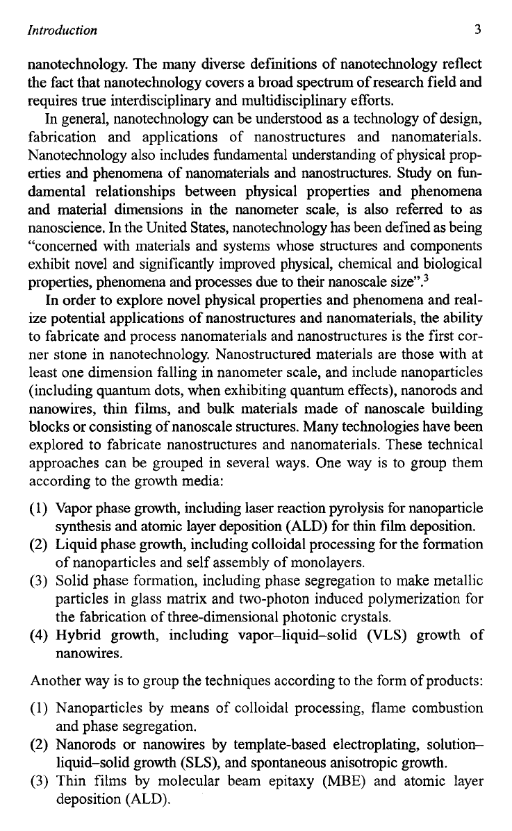
Nanotechnology deals with small structures or small-sized materials. The
typical dimension spans from subnanometer to several hundred nano-
meters.
A
nanometer (nm)
is
one billionth of a meter, or
lop9
m. Figure
1.1
gives a partial list of zero-dimensional nanostructures with their typical
ranges of dimensions.
',*
One nanometer is approximately the length
equivalent to
10
hydrogen or
5
silicon atoms aligned in a line. Small fea-
tures permit more fhctionality in a given space, but nanotechnology is
not only a simple continuation of miniaturization from micron meter scale
down to nanometer scale. Materials in the micrometer scale mostly exhibit
physical properties the same as that of bulk form; however, materials in
the nanometer scale may exhibit physical properties distinctively different
from that of bulk. Materials in this size range exhibit some remarkable
specific properties; a transition from atoms or molecules to bulk form
takes place in this size range. For example, crystals in the nanometer scale
have a low melting point (the difference can be as large as
1000°C)
and
reduced lattice constants, since the number of surface atoms or ions
becomes a significant fraction of the total number of atoms or ions and
the surface energy plays a significant role in the thermal stability. Crystal
structures stable at elevated temperatures are stable at much lower
1
Introduction
2
Nanostructures and Nanomaterials
I
05
1
o4
loo0
h
z
100
0
vl
....
10
1
Macro
particle
Micro
particle
Macro
molecule
I
T
A
Micro
molecule
I
f
4
I
Bacteria
I
I I
c
4
;
Pyrogen
V
I
I
a
Sand
j
Pollens
j.
1
Yeast
r)
Red blood
cells
:
cells
4
a
$.
I
Human
:
hair
i
V
t
Pet
+
dander
4
I
Cooking
1
smoke
V
t
Micelles
+
Gas
ion salts
b
Size
of
substance
0.
I
Fig.
1.1.
Examples
of
zero-dimensional nanostructures
or
nanomaterials with their typical
ranges
of
dimension.
temperatures in nanometer sizes,
so
ferroelectrics and ferromagnetics may
lose their ferroelectricity and ferromagnetism when the materials are
shrunk to the nanometer scale. Bulk semiconductors become insulators
when the characteristic dimension is sufficiently small (in a couple of
nanometers). Although bulk gold does not exhibit catalytic properties, Au
nanocrystal demonstrates to be an excellent low temperature catalyst.
Currently there are a lot of different opinions about what exactly is
nanotechnology. For example, some people consider the study of
microstructures of materials using electron microscopy and the growth and
characterization of thin films as nanotechnology. Other people consider a
bottom-up approach in materials synthesis and fabrication, such as self-
assembly or biomineralization to form hierarchical structures like abalone
shell, is nanotechnology. Drug delivery, e.g. by putting drugs inside carbon
nanotubes, is considered as nanotechnology. Micro-electromechanical
systems
(MEMS)
and lab-on-a-chip are considered as nanotechnology.
More futuristic or science fiction-like opinions are that nanotechnology
means something very ambitious and startlingly new, such as miniature
submarines in the bloodstream, smart self-replication nanorobots monitor-
ing our body, space elevators made of nanotubes and the colonization of
space. There are many other definitions that people working in nano-
technology use to define the field. These definitions are true to certain
specific research fields, but none of them covers the
fill
spectrum of
Introduction
3
nanotechnology. The many diverse definitions of nanotechnology reflect
the fact that nanotechnology covers a broad spectrum of research field and
requires true interdisciplinary and multidisciplinary efforts.
In general, nanotechnology can be understood as a technology of design,
fabrication and applications of nanostructures and nanomaterials.
Nanotechnology also includes fundamental understanding of physical prop-
erties and phenomena of nanomaterials and nanostructures. Study on
fun-
damental relationships between physical properties and phenomena
and material dimensions in the nanometer scale,
is
also referred to as
nanoscience. In the United States, nanotechnology has been defined as being
“concerned with materials and systems whose structures and components
exhibit novel and significantly improved physical, chemical and biological
properties, phenomena and processes due to their nanoscale size”.3
In order to explore novel physical properties and phenomena and real-
ize potential applications
of
nanostructures and nanomaterials, the ability
to fabricate and process nanomaterials and nanostructures is the first cor-
ner stone in nanotechnology. Nanostructured materials are those with at
least one dimension falling in nanometer scale, and include nanoparticles
(including quantum dots, when exhibiting quantum effects), nanorods and
nanowires, thin films, and bulk materials made of nanoscale building
blocks or consisting of nanoscale structures. Many technologies have been
explored to fabricate nanostructures and nanomaterials. These technical
approaches can be grouped in several ways. One way is to group them
according to the growth media:
(1)
Vapor phase growth, including laser reaction pyrolysis for nanoparticle
synthesis and atomic layer deposition
(ALD)
for thin film deposition.
(2)
Liquid phase growth, including colloidal processing for the formation
of nanoparticles and self assembly of monolayers.
(3)
Solid phase formation, including phase segregation to make metallic
particles in glass matrix and two-photon induced polymerization for
the fabrication of three-dimensional photonic crystals.
(4)
Hybrid growth, including vapor-liquid-solid
(VLS)
growth of
nanowires.
Another way is to group the techniques according to the form of products:
(1)
Nanoparticles by means of colloidal processing, flame combustion
and phase segregation.
(2)
Nanorods or nanowires by template-based electroplating, solution-
liquid-solid growth
(SLS),
and spontaneous anisotropic growth.
(3)
Thin films by molecular beam epitaxy
(MBE)
and atomic layer
deposition (ALD).
4
Nanostructures and Nanomaterials
(4)
Nanostructured bulk materials, for example, photonic bandgap crystals
There are many other ways to group different fabrication and processing
techniques such as top-down and bottom-up approaches, spontaneous and
forced processes. Top-down is in general an extension of lithography. The
concept and practice of a bottom-up approach in material science and
chemistry are not new either. Synthesis of large polymer molecules is a
typical bottom-up approach, in which individual building blocks
(monomers) are assembled to a large molecule or polymerized into bulk
material. Crystal growth is another bottom-up approach, where growth
species either atoms, or ions or molecules orderly assemble into desired
crystal structure on the growth surface.
by self-assembly of nanosized particles.
1.2.
Emergence
of
Nanotechnology
Nanotechnology is new, but research on nanometer scale is not new at all.
The study of biological systems and the engineering of many materials
such as colloidal dispersions, metallic quantum dots, and catalysts have
been in the nanometer regime for centuries. For example, the Chinese are
known to use Au nanoparticles as an inorganic dye to introduce red color
into their ceramic porcelains more than thousand years ag~.~~~ Use of col-
loidal gold has a long history, though a comprehensive study on the prepa-
ration and properties of colloidal gold was first published in the middle of
the 19th century.6 Colloidal dispersion of gold prepared by Faraday in
1857,7
was stable for almost a century before being destroyed during
World War
II.6
Medical applications of colloidal gold present another
example. Colloidal gold was, and is still, used for treatment of arthritis.
A number of diseases were diagnosed by the interaction of colloidal gold
with spinal fluids obtained from the patient.* What has changed recently
is an explosion in our ability to image, engineer and manipulate systems
in the nanometer scale. What is really new about nanotechnology is the
combination of our ability to see and manipulate matter on the nanoscale
and our understanding of atomic scale interactions.
Although study on materials in the nanometer scale can be traced back
for centuries, the current fever of nanotechnology is at least partly driven
by the ever shrinking of devices in the semiconductor industry and
supported by the availability of characterization and manipulation tech-
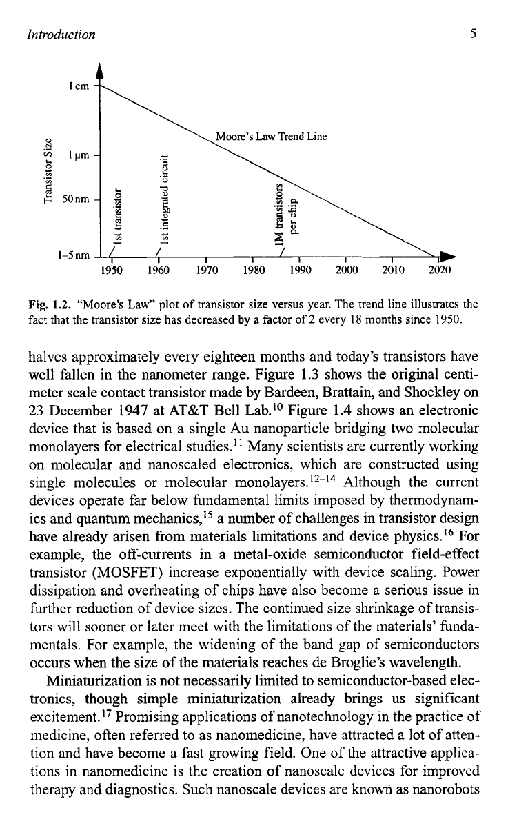
niques at the nanometer level. The continued decrease in device dimen-
sions has followed the well-known Moore’s law predicted in
1965
and
illustrated in Fig.
lL9
The figure shows that the dimension of a device
5
A
Introduction
,
Moore’s
Law
Trend
Line
r”
/ /
I
I
I
I
r)
1950
1960
1970 1980
1990
2000
2010
2020
Fig. 1.2.
“Moore’s Law” plot
of
transistor size versus year. The trend line illustrates the
fact that the transistor size has decreased
by
a factor
of
2
every
18
months since
1950.
halves approximately every eighteen months and today’s transistors have
well fallen in the nanometer range. Figure 1.3 shows the original centi-
meter scale contact transistor made by Bardeen, Brattain, and Shockley on
23 December 1947 at AT&T Bell Lab.’O Figure 1.4 shows an electronic
device that is based on a single Au nanoparticle bridging two molecular
monolayers for electrical studies.’’ Many scientists are currently working
on molecular and nanoscaled electronics, which are constructed using
single molecules or molecular
mono layer^.'^-'^
Although the current
devices operate far below fundamental limits imposed by thermodynam-
ics and quantum
mechanic^,'^
a number of challenges in transistor design
have already arisen from materials limitations and device physics.’6 For
example, the off-currents in a metal-oxide semiconductor field-effect
transistor (MOSFET) increase exponentially with device scaling. Power
dissipation and overheating of chips have also become a serious issue in
further reduction of device sizes. The continued size shrinkage of transis-
tors will sooner or later meet with the limitations of the materials’ funda-
mentals. For example, the widening of the band gap
of
semiconductors
occurs when the size of the materials reaches de Broglie’s wavelength.
Miniaturization is not necessarily limited to semiconductor-based elec-
tronics, though simple miniaturization already brings us significant
excitement.
l7
Promising applications of nanotechnology in the practice of
medicine, often referred to as nanomedicine, have attracted a lot of atten-
tion and have become a fast growing field. One
of
the attractive applica-
tions in nanomedicine is the creation of nanoscale devices for improved
therapy and diagnostics. Such nanoscale devices are known as nanorobots