Guozhong Cao. Nanostructures & Nanomaterials: Synthesis, Properties & Applications
Подождите немного. Документ загружается.

366
Nanostructures
and
Nanomaterials
physical dimension of the nanoparticles. For example, conduction elec-
trons in silver and gold have a mean free path of
40-50
nm'
l5
and will be
limited by the particle surfaces in particles of
20
nm. If the electrons scat-
ter with the surface in an elastic but totally random way, the coherence of
the overall plasmon oscillation is lost. Inelastic electron-surface collisions
would also change the phase. The smaller the particles, the faster the elec-
trons reach the surface of the particles, the electrons can scatter and lose
the coherence more quickly.
As
a result, the plasmon bandwidth increases
with decreasing particle size.'
l6?'l7
The reduction of the effective electron
mean free path and enhanced electron-surface scattering can also cor-
rectly explain the size dependence of the surface plasmon absorption as
follows.
y
is introduced as a phenomenological damping constant and is
found to be a function of the particle size"*?*
19:
(8.20)
where
yo
is the bulk damping constant and dependent on the electron scat-
tering frequencies,
A
is a constant, depending on the details of the scatter-
ing processes,
vF
is the velocity of the electrons at the Fermi energy, and
r
is the radius of the particles. This size effect is considered as an intrin-
sic size effect, since the materials' dielectric function itself is size depend-
ent. In this region, the absorption wavelength increases, but the peak
width decreases with increasing particle size (also shown in Fig.
8.21).
The molar extinction coefficient is of the order of
1
X
lo9
M-'
cm-' for
20
nm
gold nanoparticles and increases linearly with increasing volume
of
the particles.'I6 These extinction coefficients are three to four orders of
magnitude higher than those for the very strong absorbing organic dye
molecules. The coloration of nanoparticles renders practical applications
and some of the applications have been explored and practically used. For
example, the color of gold ruby glass results from an absorption band
at about
0.53
km."* This band comes from the spherical geometry of the
particles and the particular optical properties of gold according to Mie
theory112 as discussed above. The spherical boundary condition of the
particles shifts the resonance oscillation to lower frequencies or longer
wavelength. The size of the gold particles influences the absorption. For
particle larger than about
20
nm in diameter, the band shifts to longer wave-
length as the oscillation becomes more complex. For smaller particles, the
bandwidth progressively increases because the mean free path of the free
electrons in the particles is about 40nm, and
is
effectively reduced.'19
Silver particles in glass color it yellow, resulting from a similar absorption
band at 0.41 pm.120 Copper has a plasma absorption band at
0.565
pm for
copper particles in glass.12'
YO+AvF
y=

Characterization and Properties
of
Nanomaterials
3
67
Similar to nanoparticles, metal nanowires have surface plasmon reso-
nance properties.
122
However, metal nanorods exhibited
two
surface plas-
mon resonance modes, corresponding to the transverse and longitudinal
excitations. While the wavelength of transverse mode is essentially fixed
around 520 nm for Au and 4
10
nm for Ag, their longitudinal modes can be
easily tuned to span across the spectral region from visible to near infrared
by controlling their aspect ratios. It was also demonstrated that gold
nanorods with an aspect ratio of 2-5.4 could fluoresce with a quantum
yield more than one million times that of the bulk meta1.Iz3
8.4.3.2.
Quantum size effects
Unique optical property of nanomaterials may also arise from another quan-
tum size effect. When the size
of
a nanocrystal (i.e. a single crystal nanopar-
ticle) is smaller than the de Broglie wavelength, electrons and holes are
spatially confined and electric dipoles are formed, and discrete electronic
energy level would be formed in all materials. Similar to
a
particle in a box,
the energy separation between adjacent levels increases with decreasing
dimensions. Figure 8.22 schematically illustrates such discrete electronic
configurations in nanocrystals, nanowires and thin films; the electronic
X
Fig.
8.22.
Schematic illustrating discrete electronic configurations in nanocrystals,
nanowires and thin films and enlarged band gap between valence band and conduction band.
368
Nanostructures and Nanomaterials
configurations of nanomaterials are significantly different from that of their
bulk counterpart. These changes arise through systematic transformations
in the density of electronic energy levels as a function of the size, and these
changes result in strong variations in the optical and electrical properties
with si~e.'~~,'~~ Nanocrystals lie in between the atomic and molecular limit
of discrete density of electronic states and the extended crystalline limit of
continuous band.126 In any material, there will be a size below which there
is substantial variation of hndamental electrical and optical properties with
size, when energy level spacing exceeds the temperature. For a given tem-
perature, this occurs at a very large size (in nanometers) in semiconductors
as compared with metals and insulators. In the case of metals, where the
Fermi level lies in the center of a band and the relevant energy level spac-
ing is very small, the electronic and optical properties more closely resem-
ble those
of
continuum, even
in
relatively small sizes (tens or hundreds of
at~ms).l~~,~~* In semiconductors, the Fermi level lies between two bands,
so
that the edges of the bands are dominating the low-energy optical and elec-
trical behavior. Optical excitations across the gap depend strongly on the
size, even for crystallites as large as
10,000
atoms. For insulators, the band
gap between two bands is already too big in the bulk form.
The quantum size effect is most pronounced for semiconductor
nanoparticles, where the band gap increases with a decreasing size, result-
ing in the interband transition shifting to higher freq~encies.'~~-'~~ In a
semiconductor, the energy separation, i.e. the energy difference between
the completely filled valence band and the empty conduction band is of the
order of a few electrovolts and increases rapidly with a decreasing size.'31
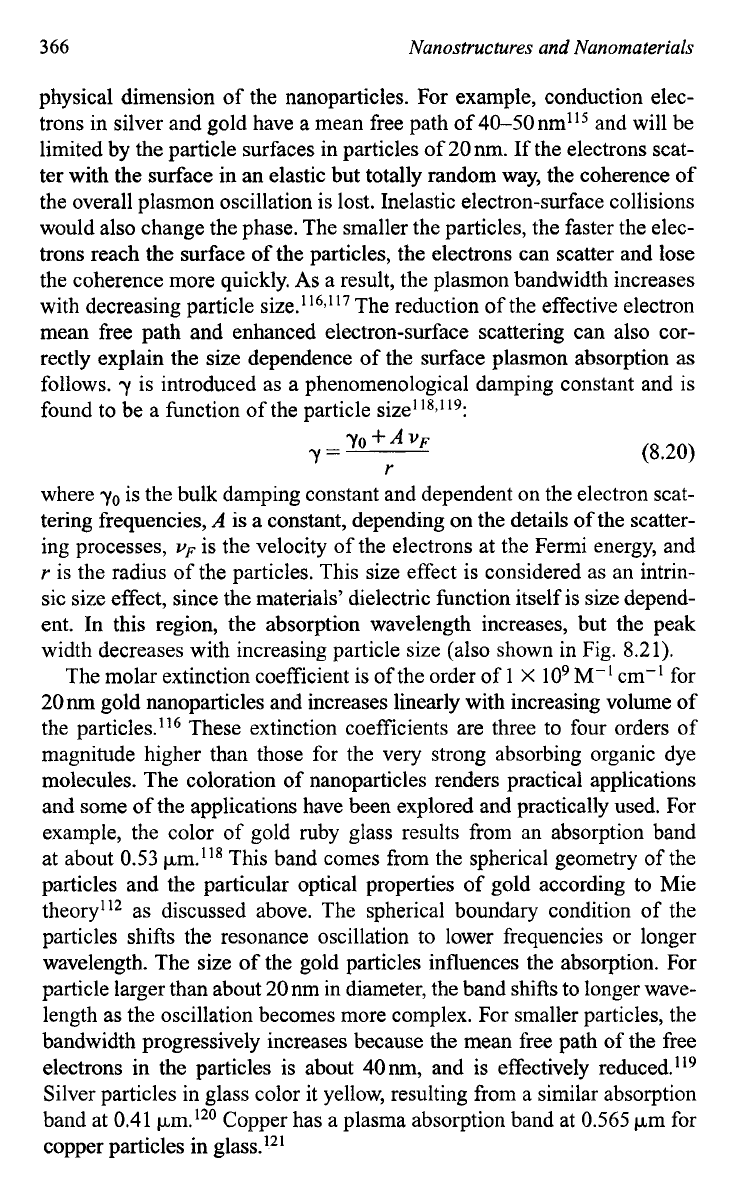
Figure
8.23
shows the optical absorption and luminescence spectra of InP
nanocrystals as a function of particle size.I3 It
is
very clear that both the
absorption edge and the luminescence peak position shift to a higher
energy as the particle size reduces. Such a size dependence of absorption
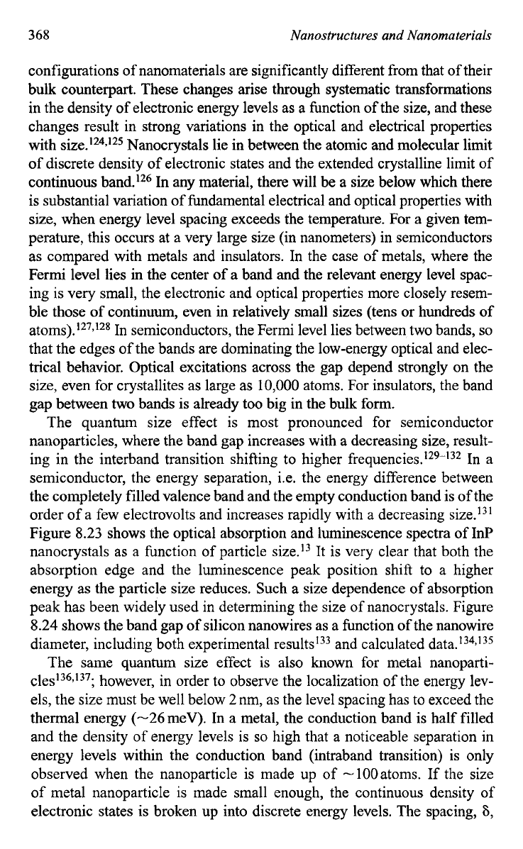
peak has been widely used in determining the size of nanocrystals. Figure
8.24
shows the band gap of silicon nanowires
as
a function of the nanowire
diameter, including both experimental results133 and calculated data.134>'35
The same quantum size effect is also known for metal nanoparti-
cles136,137; however, in order to observe the localization of the energy lev-
els, the size must be well below
2 nm, as the level spacing has to exceed the
thermal energy
(-26 meV). In a metal, the conduction band is half filled
and the density of energy levels is
so
high that a noticeable separation in
energy levels within the conduction band (intraband transition) is only
observed when the nanoparticle
is
made up of -100atoms. If the size
of metal nanoparticle
is made small enough, the continuous density
of
electronic states is broken up into discrete energy levels. The spacing,
6,
Characterization and Properties
of
Nanomaterials
369
1
.o
1.5
2.0
2.5
Energy
(eV)
Fig.
8.23.
Optical absorption and PL spectra
of
InP nanocrystals as a function
of
particle
size. The PL spectra are composed of a high-energy band edge emission band and a low-
energy trapped emission band. The insert shows additional scaled PL spectra
of
a sequence
of
samples with decreasing sizes exhibiting a smooth blue shift of the band edge emission
feature with decreasing nanocrystal size. The samples have been treated with decylamine
and were exposed to air. [A.A. Guzelian, J.E.B. Katari, A.V Kadavanich,
U.
Banin,
K.
Hamad,
E.
Juban, A.P. Alivisatos,
R.H.
Wolters, C.C. Arnold, and J.R. Heath,
J.
Phys.
Chem.
100,7212 (1996).]
d-
This
work
(Exp.)
Fig.
8.24.
The band gap
of
silicon nanowires as a function of the nanowire diameter,
including both experimental results
[D.D.D.
Ma, C.S. Lee, F.C.K. Au,
S.Y.
Tong, and
S.T.
Lee,
Science
299,
1874
(2003)l
and calculated data. [A.J. Read,
R.J.
Needs, K.J. Nash,
L.T. Canham, P.D.J. Calcott, and A. Qteish,
Phys.
Rev.
Lett.
69,
1232 (1992) and B. Delley
and
E.F.
Steigmeier,
Appl.
Phys.
Lett.
67,
2370 (1999.1
370
Nanostructures and Nanomaterials
between energy levels depends on the Fermi energy of the metal,
EF,
and
on the number of electrons in the metal,
N,
as given by138:
a=--
4EF
3N
(8.21)
where the Fermi energy
EF
is typically of the order of
5
eV in most met-
als. The discrete electronic energy level in metal nanoparticles has been
observed in far-infrared absorption measurements of gold nanoparticle.
139
At finite size, the evolution of properties of metals from the atomic level
to bulk solid is observable.
When the diameter of nanowires or nanorods reduces below the de
Broglie wavelength, size confinement would also play an important role
in determining the energy level just as for nanocrystals. For example, the
absorption edge
of
Si nanowires has a significant blue shift with sharp,
discrete features and silicon nanowires also has shown relatively strong
"band-edge" photoluminescence.
14@14*
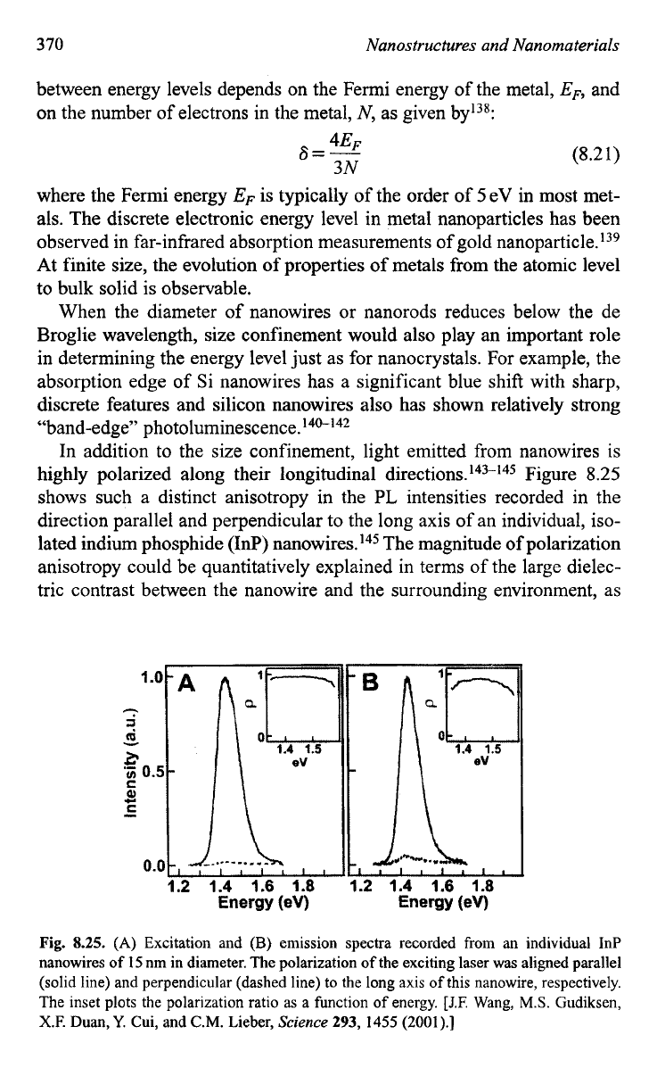
In addition to the size confinement, light emitted from nanowires is
highly polarized along their longitudinal
direction^.'^^-'^^
Figure
8.25
shows such a distinct anisotropy in the PL intensities recorded in the
direction parallel and perpendicular to the long axis of an individual, iso-
lated indium phosphide (InP) nan0~ires.l~~ The magnitude of polarization
anisotropy could be quantitatively explained in terms of the large dielec-
tric contrast between the nanowire and the surrounding environment,
as
Fig.
8.25.
(A)
Excitation and
(B)
emission spectra recorded from an individual InP
nanowires of
15
nm in diameter. The polarization
of
the exciting laser was aligned parallel
(solid line)
and
perpendicular (dashed line) to the long axis of this nanowire, respectively.
The inset plots the polarization ratio as a function
of
energy.
[J.F.
Wang,
M.S.
Gudiksen,
X.F.
Duan,Y.
Cui,
and
C.M.
Lieber,
Science
293,
1455
(2001).]
Characterization and Properties
of
Nanomaterials
371
opposed to quantum mechanical effects such as mixing of valence bands.
As
noted in Chapter
3,
there are other terms commonly used in describing
nanoparticles. Nanocrystals are specifically denoted to single crystal
nanoparticles. Quantum dots are used to describe small particles that
exhibit quantum size effects. Similarly, quantum wires are referred to as
quantum wires when exhibiting quantum effects.
8.4.4.
EIectrical conductivity
The effects of size on electrical conductivity of nanostructures and nanoma-
terials are complex, since they are based on distinct mechanisms. These
mechanisms can
be
generally grouped into
four
categories: surface scatter-
ing including grain boundary scattering, quantized conduction including
ballistic conduction, Coulomb charging and tunneling, and widening and
discrete of band gap, and change of microstructures. In addition, increased
perfection, such as reduced impurity, structural defects and dislocations,
would affect the electrical conductivity of nanostructures and nanomaterials.
8.4.4.1.
Surface scattering
Electrical conduction in metals or Ohmic conduction can be described by
the various electron scattering, and the total resistivity,
pT,
of a metal is a
combination of the contribution of individual and independent scattering,
known as Matthiessen’s rule:
PT
=
PTh
-t
PD
(8.22)
PTh
is the thermal resistivity and
pD
the defect resistivity. Electron colii-
sions with vibrating atoms bhonons) displaced from their equilibrium lat-
tice positions are the source of the thermal or phonon contribution, which
increases linearly with temperature. Impurity atoms, defects such as vacan-
cies, and grain boundaries locally disrupt the periodic electric potential of
the lattice and effectively cause electron scattering, which is temperature
independent. Obviously, the defect resistivity can be hrther divided into
impurity resistivity, lattice defect resistivity, and grain boundary resistivity.
Considering individual electrical resistivity directly proportional to the
respective mean free path
(A)
between collisions, the Matthiessen’s rule can
be written as:
111
+-
AT
ATh AD
-=-
(8.23)

372
Nanostructures and Nanomaterials
Theory suggests that
XT
ranges from several tens to hundreds of nano-
meters. Reduction in material’s dimensions would have
two
different effects
on electrical resistivity. One is an increase in crystal perfection or reduction
of defects, which would result in a reduction in defect scattering and, thus,
a reduction in resistivity. However, the defect scattering makes a minor con-
tribution to the total electrical resistivity of metals at room temperature, and
thus the reduction of defects has a very small influence on the electrical
resistivity, mostly unnoticed experimentally. The other is to create an addi-
tional contribution to the total resistivity due to surface scattering, which
plays a very important role in determining the total electrical resistivity of
nanosized materials. If the mean free electron path,
As,
due to the surface
scattering is the smallest, then
it
will dominate the total electrical resistivity:
1111
+-+-
-=-
AT
A~
AD
AS
(8.24)
In nanowires and thin films, the surface scattering of electrons results in
reduction of electrical conductivity. When the critical dimension of thin
films and nanowires is smaller than the electron mean-free path, the
motion of electrons will be interrupted through collision with the surface.
The electrons undergo either elastic or inelastic scattering. In elastic, also
known as specular, scattering, the electron reflects in the same way as a
photon reflects from a mirror. In this case, the electron does not lose its
energy and its momentum or velocity along the direction parallel to the
surface is preserved.
As
a result, the electrical conductivity remains the
same as in the bulk and there is no size effect on the conductivity. When
scattering is totally inelastic, or nonspecular or diffuse, the electron mean-
free path is terminated by impinging on the surface. After the collision, the
electron trajectory is independent of the impingement direction and the
subsequent scattering angle is random. Consequently, the scattered elec-
tron loses its velocity along the direction parallel to the surface or the con-
duction direction, and the electrical conductivity decreases. There will be
a size effect on electrical conduction.
Figure
8.26
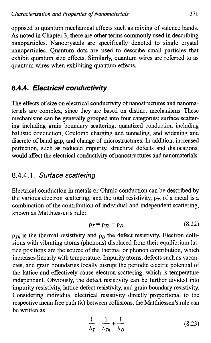
depicts the Thompson for inelastic scattering of
electrons from film surface with film thickness,
d,
less than the bulk free
mean electron path,
Xo.
The mean value of
A,
is given by:
(8.25)
After integration, we have:
(8.26)
Characterization and Properties
of
Nanomaterials
373
Fig.
8.26.
Schematic illustrating the Thompson model for inelastic scattering of electrons
from film surface with film thickness,
d,
less than the
bulk
free mean electron path,
Xo.
[J.J.
Thompson,
Proc.
Cambridge
Phil.
SOC.
11,
120
(1901).]
Finally the film resistivity,
pf,
relative to bulk values are given by:
(8.27)
From Eqs.
(8.15)
and
(8.16),
it is clear that as
d
shrinks,
A,-decreases and
p,-
increases, and there is an obvious size dependence or size effect. It should be
noted that the above model is based on an assumption that all surface scatter-
ing is inelastic and in terms of classical physics. A more accurate
quantum
theory,
known
as Fuchs-Sondheimer
(F-S)
theory, was also developed.
147,148
When the model is further improved by considering an admixture of both
elastic and inelastic contributions, with
P
being the fraction of elastic surface
scattering, an approximate formula for thin films, where
4
>>
d,
is obtained
-
3d
(1
+
2P)
pf
4x0
(8.28)
Clearly, the character of the Thompson equation [Eq.
(8.27)]
is preserved.
The fraction of elastic scattering on a surface is very difficult to determine
experimentally; however,
it
is known that surface impurity and roughness
favor inelastic scattering. It should be noted that although the surface scat-
tering discussed above is focused on metals, the general conclusions are
equally applicable to semiconductors. An increased surface scattering
would result in reduced electron mobility and, thus, an increased electri-
cal resistivity. Increased electrical resistivity of metallic nanowires with
reduced diameters due to surface scattering has been widely reported.
149
Figure
8.27
shows
the thickness dependence of electrical resistivities of
thin films as a function
of
temperat~re.'~~ In this experiment, epitaxial
films were prepared by first depositing
Co
on atomically clean silicon
sub-
strates under ultrahigh vacuum conditions and followed by vacuum anneal-
ing to promote the formation of cobalt silicide. The stoichiometry was well
controlled; the film substrate interface was found to be nearly atomically
perfect; and the outer surface was extremely smooth.
A
little dependence
3
74
Nunostructures and Nanomaterials
I
d=125;
0
197A
*
IlOOA
01
I I
I
I
0
100
200
300
400
T
(K)
Fig.
8.27.
The thickness dependence
of
electrical resistivities
of
thin films
as
a function
of
temperature.
[J.C.
Hensel, R.T. Tung,
J.M.
Poate, and
F.C.
Unterwald, Phys. Rev.
Lett.
54,
1840
(1985).]
on film thickness down to 6nm was found. Further, it was found that the
average
A,,
was
97
nm by independent low temperature magnetoresistance
measurements, and an average degree of specularity of about
90%
from
both the free surface and CoSi2-Si interface was suggested. In a polycrys-
talline material, as the crystallite size becomes smaller than the electron
mean-free path, a contribution to electrical resistivity from grain boundary
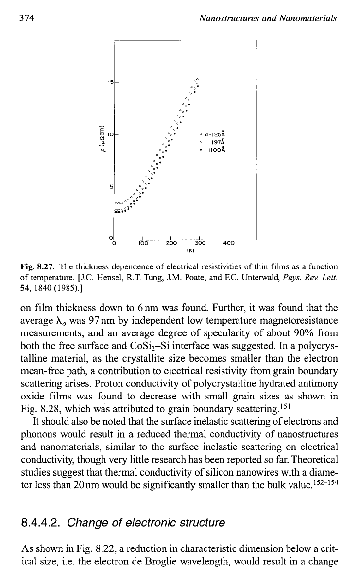
scattering arises. Proton conductivity of polycrystalline hydrated antimony
oxide films was found to decrease with small grain sizes as shown in
Fig. 8.28, which was attributed to grain boundary ~cattering.'~'
It should also be noted that the surface inelastic scattering of electrons and
phonons would result in a reduced thermal conductivity of nanostructures
and nanomaterials, similar to the surface inelastic scattering on electrical
conductivity, though very little research has been reported
so
far. Theoretical
studies suggest that thermal conductivity
of
silicon nanowires with a diame-
ter less than 20nm would be significantly smaller than the bulk vaI~e.'~
8.4.4.2. Change
of
electronic structure
As
shown in Fig. 8.22, a reduction in characteristic dimension below a crit-
ical size, i.e. the electron de Broglie wavelength, would result in a change

Characterization and Properties
of
Nanomaterials
375
10-3
h
E
x
Y
-
.-
.M
-
.p
i?
10-5
I
C
0
a
e
10-6
0
20
40
60
80
1
Relative
humidity
(96)
Fig.
8.28.
The proton conductivity
of
polycrystalline hydrated antimony oxide discs at
19.5
"C
as a function
of
relative humidity. Throughout the entire measurement region
of
humidity, the disc consisting
of
larger grains has a larger proton conductivity than
of
small
grained sample, which was attributed to grain boundary scattering.
[K.
Ozawa,
Y.
Sakka,
and
M.
Amano,
J.
Sol-Gel
Sci.
Technol.
19,
595
(2000).]
of electronic structure, leading to widening and discrete band gap. Effects
of such a change of band gap on the optical properties has been extensively
studied and discussed in the previous section. Such a change generally
would also result in a reduced electrical conductivity. Some metal
nanowires may undergo a transition to become semiconducting as their
diameters are reduced below certain values, and semiconductor nanowires
may become insulators. Such a change can be partially attributed to the
quantum size effects, i.e. increased electronic energy levels when the
dimensions of materials are below a certain size as discussed in the previ-
ous
section. For example, single crystalline Bi nanowires undergo a metal-
to-semiconductor transition at a diameter of
-52
nm155 and the electrical
resistance of Bi nanowires
of
-4Onm
was reported to decrease with
decreasing tern~erature.'~~ GaN nanowires of
17.6
nm in diameter was
found to be still semic~nducting,'~~~~~~ however, Si nanowires of
-
15
nm
became ins~1ating.l~~
8.4.4.3.
Quantum transport
Quantum
transport in small devices and materials has been studied exten-
sively.
160,161
Only a brief summary is presented below including discussions
on ballistic conduction, Coulomb charging and tunneling conduction.
Ballistic conduction
occurs when the length of conductor
is
smaller than
the electron mean-free ~ath.'~*-l~~ In this case, each transverse waveguide