Gogotsi Y. (Ed.) Nanotubes and Nanofibers
Подождите немного. Документ загружается.

Some NW materials, such as those of Group III–V materials, can be prepared via MOVPE
[12,20,21], in which deposition is carried out via the vapor phase, produced from bubbling of liq-
uid-phase precursors. Like LCG, MOVPE enables access to a broader range of inorganic binary and
ternary semiconductor materials and oxides than would be possible with gaseous sources alone.
One-Dimensional Semiconductor and Oxide Nanostructures 205
100806040200
Weight (%Ge)
Au
200
400
600
800
1000
Ge
Temperature (°C)
Nanowire
Vapor
Alloy
liquid
Metal
catalysts
Nucleation
II
Growth
III
360 °C
Alloying
L
I
I II III
FIGURE 7.2 Upper panel: schematic of VLS growth; lower panel: binary Ge–Au composition phase dia-
gram illustrating that control of temperature and partial pressure of Ge gaseous precursor can control different
phases of NW growth. (Reproduced from Xia, Y. et al., Adv. Mater., 15, 353–389, 2003. With permission.)
1/3(422)
1/3(422)
1/3(224)
1/3(242)
1/3(224)
022
1/3(422)
1/3(422)
1/3(242)
112
110
110
(a) (b)
(c)
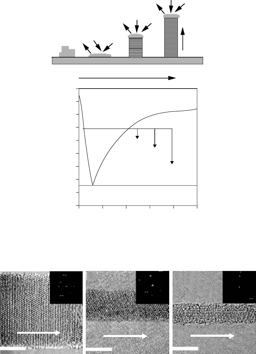
FIGURE 7.3 High-resolution transmission electron microscopy images of SiNWs with diameters of (a) 13.2,
(b) 5.7, and (c) 3.5 nm. SiNWs were grown from 10-, 5-, and 2-nm gold nanoclusters catalysts, respectively.
The scale bar is 5 nm in each panel. The NW growth axes are indicated by white arrows. (From Wu, Y. et al.,
Nano Lett., 4, 433–436, 2004. With permission.)
Copyright 2006 by Taylor & Francis Group, LLC
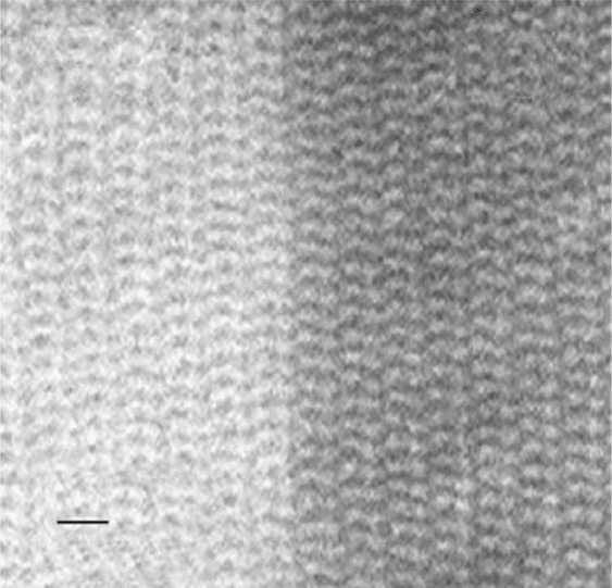
Using MOVPE and chemical beam epitaxy (CBE), researchers from Lund University have demon-
strated precise control of composition in the growth of III–V NWs, approaching monolayer sharp-
ness in axial modulation [21–24]. A representative TEM image of an axially modulated InP–InA
interface is shown in
Figure 7.4. We also note that molecular beam epitaxy (MBE) has been used
to synthesize high-quality semiconducting NWs [25]. Finally, NW synthesis by sublimation of solid
sources has been used to produce Si NWs having diameters of ~15 nm [13], and, for example,
nitrogen-doped GaN [26], AlN [27], and GaP [28] NWs. In what follows, we briefly review recent
evidence for a different growth mechanism for the synthesis of metal nanocluster-catalyzed binary
and other compound semiconductor NWs.
7.2.4 VAPOR–SOLID–SOLID GROWTH
As discussed above, the prevailing view of the mechanism of metal nanocluster-catalyzed NW growth
for both elemental and binary semiconductor NWs has been the VLS route. Though this mechanism
has been shown to be operative for metal-catalyzed elemental NW synthesis, such as Si and Ge, there
have been a number of reports for the formation of NWs on metal nanocluster-catalyst particles at tem-
peratures well below the eutectoid, and on nanoparticles having diameters much larger than those for
which the melting temperature is expected to be significantly depressed [12,29,30]. Persson et al. [23]
examined recently the question of the validity of the application of the VLS mechanism to describing
binary compound NW synthesis. Using in situ TEM of GaAs NWs as a representative system Persson
et al. demonstrated that a different mechanism is likely to be operative. The authors showed that NW
nucleation and growth may proceed by a VSS route in which the NW elemental species are trans-
ported by solid-state diffusion. This work is particularly significant because an improved understand-
ing of the growth mechanism should enable the synthesis of a broader range of combinations of NW
material components. The Lund group has confirmed that this mechanism may also be operative in
the InAs NW vapor-phase-assisted synthesis [31]. This mechanism may help explain the reported
206 Nanotubes and Nanofibers
20 Å
InAs
InP
FIGURE 7.4 Scanning transmission electron microscopy (STEM) image of interface within atomically sharp
axially modulated InAs-InP NW grown by CBE. The slow growth rate (~1 monolayer/sec) enables the forma-
tion of sharp interfaces. (From Samuelson, L. et al., Physica E, 25, 313–318, 2004. With permission.)
Copyright 2006 by Taylor & Francis Group, LLC
growth of Si–Ge alloy NWs at moderate temperatures via MCG from the vapor phase, without laser
ablation as reported by Lew et al. [32] and Redwing et al. [33].
7.2.5 CATALYST-FREE VAPOR-PHASE GROWTH
Metal-catalyzed NW growth process offers a significant degree of control in terms of diameter
selectivity and diameter dispersion. However, many semiconductor and oxide NWs can also be
grown from the vapor or solid phase in the absence of metal-nanocluster catalysts via a vapor–solid
(VS) route. These methods include oxide-assisted (OA) growth, carbothermal growth, sublimation,
PLD, and MOCVD. As the name implies, VS growth [9] involves a flowing vapor-phase precursor
produced by thermal evaporation, laser ablation, MOCVD, sublimation, or other means. Nanowires
of a number of binary-metal oxides have been grown epitaxially without metal nanocluster catalyst,
based on the VS growth mechanism.
With respect to binary-semiconductor NWs, Stach and coworkers [34] observed directly that
self-catalyzed NW growth can occur. The authors showed that by sublimation of a GaN film, liq-
uid droplets of Ga form, providing nucleation sites for the condensation of the concurrently pro-
duced GaN vapor phase. Johnson et al. [35] have reported the synthesis of pure hexagonal wurtzite
InN using indium and ammonia. In addition to syntheses of GaN [36,37] and CdS [38], Yang et al.
[39] employed vapor–solid growth to produce 20 to 100-nm-diameter single-crystalline NWs of
β
-SiC on SiC substrates. Yang and Zhang [40] reported the synthesis of 20 to 100-nm-diameter ZnS
NWs. Catalyst-free MOCVD has also been employed to produce aligned GaAs and InGaAs NWs
on partially masked GaAs and InAs substrates [41]. Pan et al. [42] reported a generalizable synthe-
sis for binary oxides, including ZnO, SnO
2
, In
2
O
3
, and CdO. Among the other binary oxides pro-
duced by VS methods are CuO [43], WO
x
[44], Ga
2
O
3
[45], Al
2
O
3
[46], and SiO
2
[47]. In addition,
Lee et al. [48] demonstrated growth of ZnO NWs on Si(100). Zhao et al. [49] reported VS synthe-
sis of SeO
2
NWs with diameters of 20 to 70 nm.
Using OA growth, Lee et al. [50] have shown that decomposition of an Si
x
O (x ⬎1) vapor pro-
duced by either thermal evaporation or laser ablation of SiO
x
targets results in a high yield of Si
NWs. The authors reported that the Si nanoparticles, which precipitate as a result of this process,
serve as nucleation sites for subsequent growth. A combination of the catalytic effect of the Si
x
O
(x ⬎1) on the NW tips, with the reduction of lateral growth by SiO
2
(formed by decomposition of
SiO) on the sides of the Si NWs, produces sustained NW growth. Stacking faults along the growth
direction of 具112典 and the availability of low-energy [51] surfaces promote the fast growth of NWs
along 具112典, and chains of nanoparticles in the case of nuclei having nonpreferred orientations.
Zhang et al. [52] have reported on a similar process developed for the synthesis of Ge NWs, pro-
ducing Ge NWs sheathed by a germanium-oxide layer. The growth of GaAs [53] and the high-tem-
perature superconductor yttrium–barium–copper oxide (YBCO) in nanorod form via laser ablation
of a YBCO target [54] are also attributed to OA growth.
Carbothermal processes represent a method for producing a large variety of metal oxide, semi-
conducting metal nitride as well as metal carbide NWs. Carbothermal methods involve the heating
of a metal oxide in the presence of activated or nanostructured carbon (e.g., carbon nanotubes
[CNTs]), producing a metal suboxide and CO. The suboxide is subsequently reacted, for example,
in O
2
, N
2
, or NH
3
to produce metal oxide or semiconducting-metal nitride NWs. This method has
been utilized to produce a wide range of NW materials, including materials such as In
2
O
3
[55],
GeO
2
[56], and GaN [57] NWs.
7.2.6 CHEMICAL SOLUTION-BASED GROWTH
Chemical solution-based methods are attractive alternatives to vapor-phase methods: the prepara-
tions are often carried out at lower temperatures. Chemical-solution methods of promoting
anisotropic crystal growth leading to 1-D nanostructures are distinguished by either kinetic control
One-Dimensional Semiconductor and Oxide Nanostructures 207
Copyright 2006 by Taylor & Francis Group, LLC
via supersaturation or by the use of coordinating ligands as capping agents. Precise control of size
and shape can often be obtained. These strategies include solution–liquid–solid (SLS), solvother-
mal, and hydrothermal methods.
The SLS method of NW growth is similar to VLS growth. Here, low melting-point metal nan-
oclusters (e.g., Sn, In, Bi) are used, and metallorganic liquid-phase precursors are decomposed
instead of vapor-phase precursors. Nanocluster-catalyst particles composed of metals with low
melting temperatures are used, and the decomposition products form an alloy with the miscible
NC-liquid droplet. Using this strategy, Buhro et al. [58–60] have synthesized single-crystalline
III–V NWs (GaAs, InAs, and GaP) at low (~200°C) temperatures. A variation of this method using
the so-called supercritical fluid-liquid solid (SFLS) method was employed by Holmes et al. [61] to
produce high-quality, defect-free, single-crystalline Si NWs. The SFLS-produced Si NWs were
seeded with 2.5-nm-diameter Au NCs and are nearly monodisperse (~4 to 5 nm in diameter).
Since the seminal work of Murray et al. [5] in synthesizing monodisperse, single-crystalline
semiconducting II–VI NCs, significant progress has been made in extending chemical solution-
based synthesis methods to produce other binary and ternary semiconducting and oxide-NC mate-
rials, and to develop rational methods for producing these NCs as shape-anisotropic 1-D
nanostructures in a wide range of material systems. Here we briefly outline the general progress in
the area of chemical synthesis of NWs and nanorods. Briefly, NC synthesis from solution involves
injection of organic precursors at elevated temperatures into a coordinating solvent. Nucleation
occurs from precipitation of the desired stable compound, and adsorption and desorption of the sur-
factant — typically one monolayer — enables deposition (and removal) of atoms on the nuclei.
Kinetic control and focusing of size is regulated by monomer concentration: for monomer concen-
tration above a solubility limit threshold, rapid growth of smaller NCs take place, and less rapid
growth of larger NCs occurs. Once the monomer concentration falls below this threshold, Ostwald
ripening takes place: NCs below a critical diameter become smaller and larger NCs grow. Capping
by the coordinating ligands also prevents agglomeration. The capping also passivates the surface of
NCs against oxidation, and improves the photoluminescence characteristics (intensity and mono-
chromic emission) by reducing or eliminating unterminated-surface bonds which lead to nonradia-
tive recombination of electron–hole pairs. Another key feature in attaining high-quality NCs — and
highly relevant for nanorod and NW synthesis using this method — is homogeneous nucleation and
its separation from the growth phase. In addition, maintaining a concentration of monomer above a
given threshold ensures rapid growth of smaller NCs and less rapid growth of larger NCs, i.e., size
focusing occurs.
Peng et al. [62] synthesized anisotropic NCs — quantum rods of CdSe — by taking advantage
of the anisotropic growth of this wurtzite-structured material when driven by an extremely high
monomer concentration. This anisotropy in growth is enhanced by the inherently
anisotropic–wurtzite structure, with preferred growth along the c-axis. The authors reported the pur-
poseful introduction of impurities to the coordinating ligand, trioctylphosphene oxide (TOPO).
Numerous other syntheses of binary semiconductors and oxide materials have been reported,
including ZnSe, Bi
2
S
3
,
γ
-Fe
2
O
3
, PZT, PbSe, PbS, ZnO, BaCrO
4
, Fe
3
O
4
, BiS, Bi
2
O
3
, Bi
2
Se
3
,
MnFe
2
O
4
, SnO
2
, cerium phosphate (CePO
4
), InAs, TiO
2
, CdTe, CoTe, NiTe, BaWO
4
, GaP, and
europium oxide [7]. A comprehensive review of oxide NW and nanorod materials and their process
routes is presented by Patzke et al. [63].
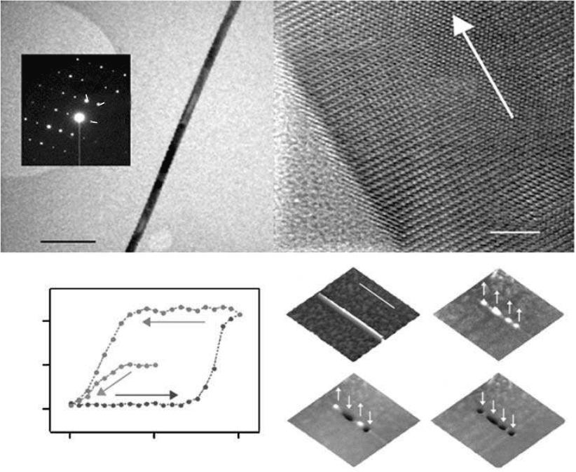
The synthesis of ternary oxide NWs, e.g., perovskite oxide NWs, has been particularly challeng-
ing. Urban et al. [64–66] demonstrated the synthesis of single-crystalline perovskite ternary oxide
(BaTiO
3
and SrTiO
3
) NWs by decomposition of metal-alkoxide precursors in oleic acid, based on a
synthetic strategy for producing monodisperse perovskite NCs developed by O’Brien et al. [67]. The
BaTiO
3
NWs possess diameters as small as 5 nm and lengths exceeding 10 µm. High resolution TEM
and converging-beam electron diffraction confirmed that the NWs are essentially defect-free, single-
crystalline, and the c-axis is oriented along the long axis of the NW
(Figure 7.5). Xu et al. [68]
employed a hydrothermal synthesis in the presence of polyvinyl alcohol and polyacrylic acid, to
208 Nanotubes and Nanofibers
Copyright 2006 by Taylor & Francis Group, LLC
produce single-crystalline PbZr
0.52
Ti
0.48
O
3
NWs. Of particular significance is that the BaTiO
3
NWs
produced by Urban et al. enabled more detailed investigations into ferroelectricity in nanostructured
materials [65,66,69]. Electrostatic force microscopy of these NWs reveals that the NWs possess sta-
ble ferroelectric (FE) polarizations, which can be reproducibly reoriented perpendicular to the NW
axes. As shown in Figure 7.5, these NWs exhibit FE hysteresis, and polarizations in these NWs can
be independently induced and manipulated. The FE domains in these NWs represent the smallest vol-
umes of stable FE reported to date. Subsequent studies have revealed distinct scaling behavior of the
evolution of FE phase transition temperature, and further fundamental insights into the origins of FE
stability in nanostructured and ultrathin-FE films. Our findings and the results of our investigations,
combining density-functional theoretical simulations with experiments, will be reported in a forth-
coming publication [70].
7.2.7 TEMPLATE-ASSISTED GROWTH
Another route for obtaining 1-D nanostructures involves the use of nanostructured templates, which
act as a host material into or onto which NWs (or alternatively NTs) of a wide range of materials
can be grown. For example, Ge NWs have been formed via deposition onto periodic corrugations
One-Dimensional Semiconductor and Oxide Nanostructures 209
(002)
(112)
(110)
200 nm
5 nm
[001]
20
0
−20
−10 10 0
∆/ × 10
6
V
tip
(V)
1 µm
FIGURE 7.5 Upper panel: electron microscopy images of a representative single-crystalline BaTiO
3
NW.
Results from high-resolution transmission electron microscopy, and converging beam electron diffraction
(inset), collected at a number of locations along more than 50 NWs confirm that each NW is an essentially
defect-free single-crystalline perovskite NW. Lower panel: FE hysteresis of individual FE domain oriented per-
pendicular to the axis of an 11-nm-diameter NW (left), and independent manipulation of FE polarization
within an individual BaTiO
3
NW (right), measured by scanning probe microscopy. (From Urban, J.J. et al.,
Adv. Mater., 423–426, 2002; Spanier, J.E. et al., in Nanowire Materials, Vol. 1, Wong, Z.L., Ed., Kluwer,
Boston, MA, 2002; Yun, W.S. et al., Nano Lett., 2, 447–450, 2002. With permission.)
Copyright 2006 by Taylor & Francis Group, LLC
(V-grooves produced by anisotropic etching in Si[100]) [71]. Salamo and coworkers [72] have used
MBE on high-index GaAs surfaces to promote the assembly of (In, Ga)As NWs and other nanos-
tructures during deposition. Following the growth or deposition into templates, selective etchants
can be used to isolate NWs. Among the advantages for this method is straightforward alignment of
NWs using template material having columnar pores, and the wide flexibility in deposition meth-
ods, including metal-catalyzed growth, catalyst-free growth from the vapor or liquid phases, elec-
trochemical methods, and solution-gelation (sol-gel). In addition, NW diameter is controlled by the
template-pore diameter. A principal disadvantage, however, is that the NWs produced using tem-
plate-assisted growth (TAG) are frequently not single crystalline. Moreover, the lower limit of
diameter of NWs is governed by the template-pore diameter, and some of the hierarchal structures
that can be produced via MCG may not be as easily prepared using TAG. In addition, aspect ratios
of TAG may be limited by mass transport. Among templates, two types of nanoporous-membrane
templates are frequently used: anodic aluminum oxide, (AAO) [73–76] and porous-polymer films
[77]. Pathways for the production of inorganic NWs include CNTs [78] and zeolites [79]. To pro-
duce AAO templates, aluminum films are electrochemically oxidized, and local etching takes place
producing pores that have local hexagonally close-packed ordering. Subsequent anodization of the
film leads to columnar pores with relatively monodisperse diameters ranging from 5 nm to ⬎100
nm, depending upon preparation conditions, e.g., electrolyte composition and concentration, and
anodization voltage. Such template materials (e.g., Anodisc™) can be obtained commercially via
Whatman™ or prepared. Shingubara [80] has presented a review of the use of AAO templates for
the preparation of nanomaterials. Polymer films having track-etched channels are formed by irra-
diation of heavy ions from nuclear fissions [81]. In many cases, following deposition, the NWs can
be isolated by selective etching of the template; often an appropriately selected acidic solution pro-
vides the necessary selective etching. A diverse number of materials, including metals, semicon-
ductors, and binary oxides have been deposited in templates via vapor phase, electrochemical
means, or sol-gel methods.
Lew et al. [82], Lew and Redwing [83], and Redwing et al. [33] demonstrated that high-qual-
ity, single-crystalline Si and SiGe NWs can be produced using AAO templates with a metal cata-
lyst. In contrast to template-free MCG, in this case, the NW diameter is controlled by the template
diameter. This process has several notworthy features: it provides one possible route for growth-
aligned NWs; it enables investigation of growth mechanisms and kinetics in the absence of catalyst-
particle size-driven considerations. The demonstration of SiGe NW growth suggests the possibility
of producing more complex NW materials and compositions, such as Si
x
Ge
1⫺x
NWs, whose com-
position is controlled. Template-based methods have not been limited to AAO and polymer-based
templates: for example, Han et al. [78] used CNTs as templates to facilitate the syntheses of single-
crystalline GaN and Si
3
N
4
NWs.
Al-Mawlawi and coworkers [84] demonstrated synthesis of CdS NW arrays via electrodeposi-
tion using AAO. Electrochemical methods typically yield NWs, which are polycrystalline and not
single crystalline; for many applications, however template-assisted electrochemical deposition
offers a rather easy route for synthesizing 1-D structures. Often limitations due to mass transport —
well understood from the electrodeposition through or in vias in top-down semiconductor device
processing — can be ameliorated by use of pulsed or alternating current (AC) electrodeposition
techniques. In selected cases, high-quality and even single-crystalline NWs have been produced
using this technique. Another attractive (though not exclusive) feature of electrodeposition is that
multiple species can be reduced and deposited at selected over potentials, enabling the formation of
compositionally segmented NWs within a single electrochemical bath.
For several decades, sol-gel methods [85] have represented an attractive, low-cost method for
producing both planar and nonplanar-thin films of a diverse number of materials, including binary,
ternary, and quaternary oxides, and binary semiconductors. For more than a decade, sol-gel methods
have been used with nanoporous templates to produce 1-D nanostructures, both NWs and NTs. In
nearly all cases, these nanostructures are polycrystalline in nature with varying degrees of control of
210 Nanotubes and Nanofibers
Copyright 2006 by Taylor & Francis Group, LLC
orientation or texture, though there have been some exceptions. For example, Miao et al. [86]
reported the synthesis of single-crystal anataste TiO
2
NWs via an electrochemically enhanced sol-gel
route. Frequently, the instability of polymeric precursors in air requires sol-gel methods to be carried
out in an anhydrous environment. Here, the commercially available, air-stable polymeric precursors
for sol-gel processing routes have been helpful in furthering the research in the synthesis and char-
acterization of nanomaterials.
7.2.8 SELECTED OTHER METHODS
One particularly novel template-like method for producing a wide range of single-crystalline NW
materials, developed by Belcher and coworkers [87], is through the use of a virus-based scaffold.
Selected peptides that were shown to exhibit control of composition, size, and phase during
nanoparticle nucleation were expressed on a highly ordered capsid of a bacteriophage, providing a
template for directed synthesis of NWs. Variation of the synthetic route via substrate-specific pep-
tides through the virus offers a new material tunability not previously available. Other routes are
possible as well. For example, an additional route particularly suited for the preparation of metal
oxide NWs is the thermal oxidation of metal NWs produced by template-assisted or chemical solu-
tion-based methods, and Tang et al. [88] have shown that dipole-dipole interactions can be used to
facilitate the assembly of monodisperse CdTe NCs into highly crystalline NWs with uniform sizes.
7.3 HIERARCHAL COMPLEXITY IN 1-D NANOSTRUCTURES
Control of NW diameters, diameter dispersion, and crystallographic and physical orientation are
important features for fundamental investigations of size-scaling effects and for enabling the use of
NWs as building blocks for nanotechnology. Moreover, synthesis routes for preparing other quasi-
1-D topologies may provide new insights into mechanisms of nanostructure growth and new mate-
rial platforms for a range of technologies. In addition to the well-known effects of finite size on
electronic-band structure, the effects of finite size on nonlinear-optical properties, electrical and
thermal conductivity, ferroelectricity, ferromagnetism, superconductivity, phonons, and on the evo-
lution of phase-transition temperatures and pressures, and susceptibility behavior, are all areas of
intense investigation.
7.3.1 CONTROL OF DIAMETER AND DIAMETER DISPERSION
While several methods permit synthesis of NWs with lengths of many microns or even tens of
microns, and with diameters of the order of 10 nm and higher, controlled and reproducible growth
of NWs with smaller diameters (⬍5 nm) and with narrow diameter dispersion has been more chal-
lenging. Control of the relative growth rates in axial and radial directions is an important feature in
enabling access to a range of NW architectures. As pointed out by Wagner [9] for the VLS mecha-
nism, it is hypothesized that several factors are significant in determining the diameter of the NWs.
The size(s) of the catalyst nanoclusters is important, since the eutectic-droplet size for nucleation is
defined by these. Secondly, the temperature will profoundly affect the diameter (and in some cases
also the shape), since the solubility of the precursor reactant in the nanocluster will alter the eutec-
tic droplet size, which in turn will alter the NW diameter. Finally, a vapor pressure of the precursor
reactant in excess of the critical value at which deposition of the precursor reactant onto the NW
surface (as opposed to the eutectic droplet) takes place, will also have the effect of producing radial
as well as axial NW growth.
Gudiksen and Lieber [89] and Gudiksen et al. [90] demonstrated that Si NWs with control of
mean diameter and with relatively narrow size dispersions can be synthesized: 5 (4.9 ⫾ 1.0), 10 (9.7
⫾ 1.5), 20 (19.8 ⫾ 2.0), and 30 (30.0 ⫾ 3.0) nm-diameter Au colloid was used to produce Si NWs
with diameters of 6.4 ⫾ 1.2, 12.3 ⫾ 2.5, 20 ⫾ 2.3, and 31.1 ⫾ 2.7 nm, respectively. The authors
One-Dimensional Semiconductor and Oxide Nanostructures 211
Copyright 2006 by Taylor & Francis Group, LLC
point out that the dispersion in diameters for each size group is comparable to that of the catalyst
particles, providing further evidence of the distinct role of nanocluster size in determining NW
diameter.
Single-walled CNTs have attracted significant interest because they behave as 1-D metallic con-
ductors or semiconductors with respect to electronic carriers. With regard to NWs, one challenge
has been to produce “molecular wires” in which the diameter of the NWs is as small as possible —
approaching a single chain of atoms. Such wires would find application, for instance, to the prob-
ing of size scaling and dimensionality effects in electronic transport, for extreme carrier or phonon
confinement, or, for example, unique signatures in metal-insulating transitions associated with
Peierls distortions in 1-D. In principle, the minimum NW radius is governed by equilibrium ther-
modynamics, namely that r
min
⫽ 2
σ
LV
V
L
/RT ln
σ
, where
σ
LV
is the liquid–vapor surface-free
energy, V
L
the molar volume of liquid, and
σ
the vapor-phase supersaturation. This suggests that
nucleation and growth of ultranarrow-diameter NWs may be achieved using a higher partial pres-
sure of precursor for the nucleation phase, followed by lower partial pressure for the growth phase.
This has recently been applied by Wu et al. [19] in the VLS synthesis of molecular-scale Si NWs
as shown in
Figure 7.3.
In chemical solution-based NW synthesis, however, the control of diameter can be superior to
those produced through VLS. For example, as of now, several investigators have applied size-selective
precipitation methods originally developed by Murray et al. [5], to produce a growing number of
nanostructured materials with size dispersion of the order of one monolayer. Peng et al. [62] have
shown that the CdSe nanorods possess narrowsize dispersions, as demonstrated by the periodic
ordering of these structures. Control of diameter and diameter dispersion has been shown in binary-
oxide NW systems. For example, O’Brien and coworkers [91,92] reported on an aqueous solution-
based chemical synthesis producing ZnO NWs with monodisperse-diameter NW yields, with
diameters as narrow as 2 nm; the authors also reported on the measurement of strong excitonic
confinement in these structures.
7.3.2 CONTROL OF SHAPE: NOVEL TOPOLOGIES
One of the significant features of inorganic-nanomaterial synthesis by surfactant-mediated chemi-
cal routes is the possibility of controlling the size and shape of nanostructures, thereby effectively
manipulating their properties. Manna et al. [93] demonstrated the growth of a range of nanostruc-
tures by varying the relative concentrations of two types of surfactants–TOPO and hexylphospho-
nic acid (HPA) –– and systematically varying the monomer concentration with time. The HPA
serves to accentuate the difference between growth rates on different crystal faces. Different sys-
tematic variations yield long rods, arrow-shaped NCs, teardrop-shaped NCs, tetrapods, and den-
dritic tetrapods. Manna et al. have also reported [93] that differences between wurtzite and rocksalt
free energies and surface energetics govern the evolution of some of these structures — particularly
stacking faults in the tetrapods. They have explained the topology in terms of abrupt changes in the
crystal structure, from wurtzite in the rod segments to rock salt in the sphere-like vertices. Very
recent investigations by Manna and coworkers, however, have indicated that this multiphase
description of the tetrapod, and the corresponding model of their formation may not be valid: rather,
it seems that the tetrapod nanostructures may consist of single phase, and that it is likely that the
formation of twins plays a significant role in the unique evolution of their topologies [94].
The control of the relative axial and radial growth rates is the basis for the synthesis of coaxial, or
core–shell nanostructures as discussed above. In our laboratory at Drexel, we have demonstrated the
growth of apex-angle-controlled crystalline Si nanocones (Si NCs) and Ge nanocones (Ge NCs) of
diamond-hexagonal phase through simultaneous control of axial and radial growth rates using metal-
catalyzed CVD; we have also synthesized single-crystalline Ge nanosprings and characterized its
composition and crystallinity with electron microscopy and Raman scattering. As shown in
Figure 7.6,
the Si NCs are tapered polyhedra, possessing hexagonal cross sections. They are typically several
212 Nanotubes and Nanofibers
Copyright 2006 by Taylor & Francis Group, LLC
microns in base diameter, and the radius of curvature at the tip is as small as 1 to 2 nm. Significantly,
these nanocones are of the diamond-hexagonal polymorph, and the taper angles can be tuned during
growth. These Si NCs may offer new opportunities as scanning probes and as central components in
single-molecule sensing. Details on the synthesis and characterization of the unique structural, opti-
cal, and other properties will be presented in several forthcoming publications [95,96].
7.3.3 OTHER BINARY OXIDE 1-D NANOSTRUCTURES
An incredibly diverse range of 1-D nanostructure topologies composed of binary oxides has been
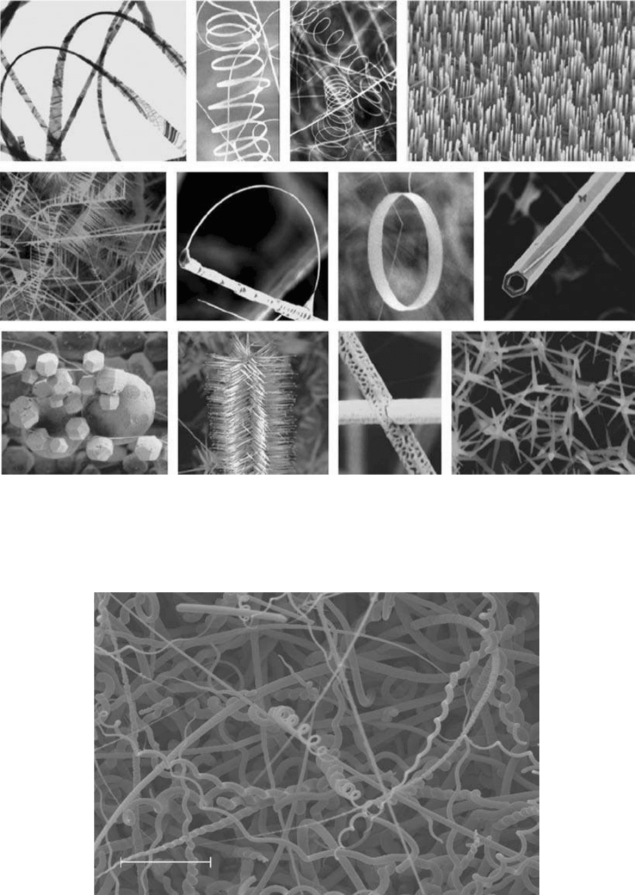
developed by Z. L.Wong and coworkers at Georgia Tech, using solid-state thermal sublimation and
other techniques. A representative group of these 1-D nanostructures is shown in
Figure 7.7. Briefly,
oxide powder is placed in the hot zone of a furnace, and ions from the vapor-phase condense onto a
nearby substrate in a lower temperature zone of the furnace. The control of growth kinetics of the polar
surface-dominated nanostructures as well as the use of templates and metal nanoclusters leads to the
synthesis of a wide range of nanostructured topologies, including nanobelts, nanoribbons, nanorings
and nanobows [97], nanosaws [98,99], and nanohelixes [100] –– comprehensive reviews are
presented in [101–104]. While this diverse class of nanostructures possess a common feature in that
each is composed of a binary oxide with polar surfaces, we have recently identified CVD-based syn-
thesis methods in our own laboratory to produce similar crystalline-elemental nanostructures, includ-
ing Ge nanohelixes and tree-branched Ge nanostructures possessing sixfold branching symmetry
[105]. Our findings of synthesis conditions producing crystalline nanosprings in a material without
polar surfaces (e.g., Ge as shown in
Figure 7.8) suggests that mechanisms other than polar surface-
specific energies and piezoelectricity may also be operative in the formation of one or more of the
binary-oxide nanostructures, this is an area of ongoing investigation by our group [105].
7.3.4 HIERARCHAL 1-D NANOSTRUCTURES
The integration of two or more semiconductor or other materials and the controlled incorporation
of dopants within individual components of nanostructures are essential characteristics of the
advancing development of NWs as building blocks for nanotechnology. Homo- and heterojunctions
within individual NWs enable fabrication of bipolar devices within individual NWs, opening up
possibilities for light-emitting diodes, photodetectors, and band gap-engineered devices within indi-
vidual NWs, and even NW-based superlattices.
One-Dimensional Semiconductor and Oxide Nanostructures 213
5 µm
1 µm
5 nm
FIGURE 7.6 Silicon nanocones (Si NCs) formed by metal nanocluster-catalyzed CVD. The left panel shows
an array of nanocones, which are tapered polyhedra, possessing hexagonal cross sections. These Si NCs are
typically several microns in base diameter. As shown in the panel on the right, the radius of curvature at the tip
is as small as 1 to 2 nm. Though not shown, control of conical angle and its dispersion has also been achieved.
(From Cao, L. et al., J. Am. Chem. Soc. in press, 2005. With permission.)
Copyright 2006 by Taylor & Francis Group, LLC
214 Nanotubes and Nanofibers
FIGURE 7.7 Representative polar surface-dominated, single-crystalline, zinc oxide 1-D nanostructures.
(From Wang, Z.L., Mater. Today, 26–33, 2004. With permission.)
10 µm
FIGURE 7.8 Scanning electron micrograph of crystalline germanium nanosprings. The formation of
nanosprings having inversion symmetry may generate further debate on the formation mechanisms of these
and similar structures, in both polar and nonpolar crystalline materials. (From Martin, R.R. et al., submitted.
With permission.)
Copyright 2006 by Taylor & Francis Group, LLC