Fahlman B.D. Materials Chemistry
Подождите немного. Документ загружается.

(e.g., Formvar,
[20]
Collodion (nitrocellulose),
[21]
Butvar B98
[22]
) films are first
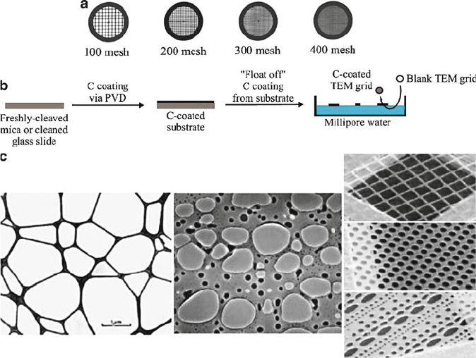
deposited onto a glass microscope slide or mica surface, and floated off onto the
surface of filtered water. For polymer films, the pre-cleaned glass/mica surface is
simply immersed in a 0.3% ethylene dichloride solution of the polymer. By contrast,
carbon films are deposited onto the glass/mica surface through sputter coating. The
coated glass/mica substrate is allowed to dry completely, scored with a razor blade,
and slowly immersed into a container of distilled water. When water reaches the score
marks, surface tension effects cause the film to be pulled from the glass/mica, resulting
in a floating film on the surface of the water. Grids are then dunked into the water and
brought up underneath the floating film, lifted out of the water, and allowed to air-dry
completely. The coated grids are stored in a dry, dust-free environment.
The typical thickness of amorphous carbon films is 2–5 nm, whereas polymer
films have thicknesses on the order of 30 nm. As you might expect, all plastic films
are subject to decomposition by the electron beam. Sometimes, this exposure also
causes further crosslinking that will cause the film to shrink and become more
brittle. The surface adsorption characteristics of support films vary quite signifi-
cantly between polymer and carbon varieties. In general, polymer films possess
hydrophilic characteristics whereas carbonaceous support films are hydrophobic.
Figure 7.9. (a) A comparison of TEM grid mesh sizes; (b) Illustration of the “float off” method to prepare
carbon-coated TEM grids; (c) Comparison of a lacey carbon coating with holey carbon films deposited
onto TEM grids.
598 7 Materials Characterization
For the imaging of nanomaterials, it is most desirable to have a support film that
resembles a piece of lace, featuring many holes on the surface. In this manner, nano-
structures such as nanotubes or nanowires are held on the surface of the support
film, with unobstructed imaging made possible through holes in the film surface
(Figure 7.9c). Such “holey” or “lacey” grids are made from plastic film suspensions
to which water or glycerin has been added. Due to the microemulsions created in
the solution, when the film is dried, thousands of tiny holes are left in the support
film. In this way, the coating itself acts like a mesh grid with the thousands of very
tiny open viewing areas.
Due to the high vacuum environment and bombardment of the sample with high-
energy electrons, not all samples are appropriate for TEM characterization. In partic-
ular, any sample comprising a volatile organic compound, or those containing residual
solvents, must be dried using freeze–pump–thaw procedures, or supercritical fluid
media. Failure to do so will result in collisions between the electron beam and stray
gaseous molecules in the column, resulting in defocusing of the beam and a reduction
in image quality. Further, the decomposition of organic matter can severely contami-
nate the microscope column – especially in finely machined regions such as apertures
and pole pieces resulting in blurry images. Some samples may not be directly
analyzed even following drying procedures, due to their instability toward the focused
electron beam. For these samples (e.g., biological), the specimen is mounted within a
plastic support resin, and very thin pieces of the composite are shaved off using an
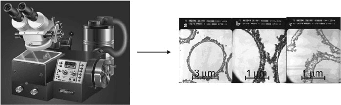
ultramicrotome fitted with a diamond, sapphire, or glass knife (Figure 7.10).
TEM grids of solid samples are typically prepared by pipetting a few drops of a
solution containing the suspended solid onto a grid, and allowing it to air-dry.
Alternatively, the suspension may be blown onto a grid using an aerosol delivery
device (Figure 7.11). If the solid is too thick, or comprises relatively large granules,
the mater ial may be embedded within a polymeric matrix and cut into thin cross
sections. The best embedding medium permits thin sectioning with the least damage
Figure 7.10. Sectioning of a TEM sample using an ultramicrotome instrument. Shown is an
ultramicrotome instrument with a built-in nitrogen cryogenic system, used to section samples with a
thickness of 25 nm–5 mm.
[23]
Also shown is a TEM image of polymer capsules that have been sectioned
using an ultramicrotome instrument. Image reproduced with permission from Dai, Z.; Mohwald, H.
Langmuir 2002, 18, 9533. Copyright 2002 American Chemical Society.
7.2. Electron Micros copy 599

during preparation, and gives the least interference during microscopy. While
early embedding media included gelatin and paraffin, the <100 nm sections that
are required for electron microscopy were not possible to cut using any of these
media. Nowadays, polymers such as methacrylates, epoxy and polyester resins are
typically employed for sectio ning applications, since they are nontoxic, inexpensive,
and strong enough to withstand very thin mechanical sectioning. For methacrylates,
the degree of final block hardness can be predictably controlled by mixing methyl
(hard) and n-butyl (soft) functionalities. However, with respect to electron beam
stability, epoxy resins are by far superior to both methacrylates and polyester resins.
The “best” section thickness not only depends on the electron opacity of the
sample, but also on the operating conditions of the TEM . In general, the higher the
accelerating voltage, the thicker the sample cross section may be. For instance,
epoxy-based sections of up to 250 nm thick may be used for standard TEM analyses ,
operating at 100 kV. However, section thicknesses in the range of 50–60 nm are
typically used for TEM analysis, in order to improve the resolution through reduced
electron scattering.
A recent alternative to (ultra)microtoming is the use of a focu sed-ion beam (FIB)
to etch/mill away undesired portions of the sample (Figure 7.12). The most common
beam is gallium ions from a liquid gallium source, with an energy of ca . 30 keV.
Extreme control over the resultant cross section is afforded by varying the beam
current/energy, and scanning speed of the ion beam. This techniq ue is especially
useful for the study of polymer films that have been deposited onto hard inorgani c
substrates – using a FIB/lift-out method.
[24]
Typically, a dual-beam FIB/SEM is
used for sample preparation, which affords real-time monitoring of FIB sectioning
(Figure 7.12b). A more recent use of a FIB instrument is nanofabrication. In
particular, in situ CVD of a thin film may be deposited through the introduction
of a co-reactant precursor gas during ion bombardment (Figure 7.12c). It should
be noted that in contrast to ultramicrotomy, FIB preparation does not induce
Figure 7.11. Photo of a glass aerosol delivery system used to spray solvent-suspended particulates onto a
TEM grid.
600 7 Materials Characterization
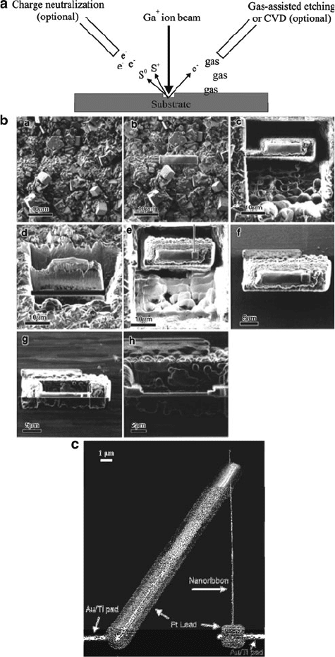
Figure 7.12. Applications for focused-ion beam (FIB). Shown is (a) general illustration of the technique,
with a gallium ion source and emission of secondary electrons, as well as charged ions and atoms from the
substrate surface (S
þ
and S
0
, respectively). The optional “charge neutralization” electron beam is used for
in situ imaging of a surface during FIB (dual-beam FIB/SEM). The images shown in (b) represent the
sectioning of a zeolitic membrane (images c and d illustrate FIB milling to a depth of 20 mm, and cutting
off the bottom surface; latter images show the manipulation of the milled target and further sectioning by
FIB).
[26]
The SEM image in (c) illustrates the use of FIB for nanofabrication – the selective deposition of
Pt contact leads onto the ends of a Ga
2
O
3
nanowire.
[27]
7.2. Electron Micros copy 601
mechanical stress on the sample surface, which often leads to deformation and
interfacial debonding. However, the high-energy radiation may result in other surface
modifications such as amorphization, shrinkage, and bond cleavage – especially for
“soft,” polymeric-based samples.
[25]
Oftentimes, a lack of image contrast in TEM results from the analysis of very thin
sections (e.g., <30 nm), or samples comprising light elements (e.g., hydrocarbons, B,
Li, etc.). In order to increase the contrast, elements of high atomic weight are intro-
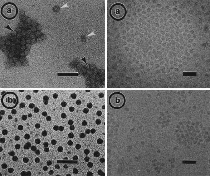
duced to selective regions of the sample – a process referred to as staining (Figure 7.13).
Due to their high electron density, staining agents are better able to stop or deflect
the beam of electrons, whereas elements of low weight allow the beam to pass
through relatively unimpeded. Electron staining falls into one of two categories:
(i) Positive staining – contrast is imparted to the sample.
(ii) Negative staining – contrast is imparted to the area surrounding the sample.
Figure 7.13. (Left, a) TEM image of G10 PAMAM dendrimers stained with 2% methylamine tungstate,
showing both positively (white arrows) and negatively (black arrows) stained regions. (Left, b) TEM
image of G9 PAMAM dendrimers positively stained with sodium phosphotungstate, showing little
agglomeration. (Right, a, b): TEM images showing the lack of contrast from unstained G10 PAMAM
dendrimers, imaged in vitrified water using cryo-TEM. The scale bar for all images is 50 nm. Reproduced
with permission from Jackson, C. L.; Chanzy, H. D.; Booy, F. P.; Drake, B. J.; Tomalia, D. A.; Bauer, B. J.;
Amis, E. J. Macromolecules 1998, 31, 6259. Copyright 1998 American Chemical Society.
602 7 Materials Characterization
The most com mon staining agents are aqueous solutions (ca. 2 wt% concentra-
tion) of OsO
4
(osmium tetroxide), RuO
4
(ruthenium tetroxide), UO
2
(CH
3
COO)
2
·
2H
2
O (uranyl acetate), Pb(C
6
H
2
O
7
)
2
·3H
2
O (lead citrate), or Na
3
[PW
12
O
40
]·
30H
2
O (sodium phosphotungstate). Due to the presence of heavy metals, these
agents are considerably toxic and must be handled/disposed with great care.
Whereas most of these agents interact most strongly with amino and phosphate
groups, lead ions preferentially interact with hydroxyl groups. For biologi cal stain-
ing, it has been widely shown that OsO
4
interacts more readily with lipids than
proteins, resulting in a structure-specific staining agent. The use of lead citrate
requires special considerations due to its high sensitivity to CO
2
; hence , NaOH is
often used as a CO
2
-scavenger for the aqueous staining solution.
Non-imaging applications for TEM
Due to the high spatial resolution and predictive scattering modes, TEMs are often
employed to determine the three-dimensional crystal structure of solid-state materials.
Thus, TEM may be considered as complementary to conventional crystallographic
methods such as X-ray diffraction. Since the wavelength of an accelerated electron in
a TEM is much smaller than an X-ray beam, the Ewald sphere (see Chapter 2 –
Figure 2.44; radius ¼ 1/l) is significantly larger for electron diffraction relative to
X-ray diffraction studies. As a result, electron diffraction yields much more detailed
structural information of the crystal lattice. Information such as lattice parameters and
atomic positions in a crystal may be obtained through analyzing the in situ electron
diffraction pattern from a specimen size of ca. >400 nm (>100 nm for a field emission
source). This technique is denoted as selected area electron diffraction (SAED,
Figure 7.14).
[28]
In addition, the lenses within a TEM allow one to alter the orientation
of the incoming electron beam, from a parallel beam to a cone-shaped beam. The latter
orientation is known as convergent beam electron diffraction (CBED), and allows
one to conduct a diffraction experiment over many incident angles simultaneously to
reveal the full three-dimensional reciprocal lattice of the crystal.
[29]
In the same manner as X-ray diffract ion (see Chapter 2), by examining the
systematic absences of the electron diffraction pattern, one may easily determine
the appropriate Bravais lattice as well as any screw axes and glide planes that are
present in the crystal lattice. Since TEM is more user-intensive, involves significant
sample preparation, and often results in sample damage from the high-energy
electron beam, highly automated X-ray and neutron (useful for light elements such
as H) diffraction methods are the preferred methods to yield structural information
from a bulk crystalline solid. However, if structural information is desired from an
individual nanocrystal, TEM/SAED is the best alternative.
[32]
Before leaving the subtopic of electron diffraction, it should be noted that two
other techniques known as low-energy electron diffraction (LEED)
[33]
and reflection
high-energy electron diffraction (RHEED)
[34]
may also be used to gleam structural
information from a crystalline sample. Both techniques are performed independent
of a TEM instrument, and utilize an electron gun and fluorescent screen to show the
structure and morphology of a crystal surface. The RHEED technique uses a high
7.2. Electron Micros copy 603
accelerating voltage and low impact angle in order to focus the electrons to the first
few atomic layers of the crystal surface. This techniq ue may be used to monitor
crystal growth in real time, or to probe the surface adsorption properties for sensor
development. For beam -sensitive crystalline samples (e.g., organic thin films),
either LEED or microchannel plate (MCP)–RHEED may be used; the latter features
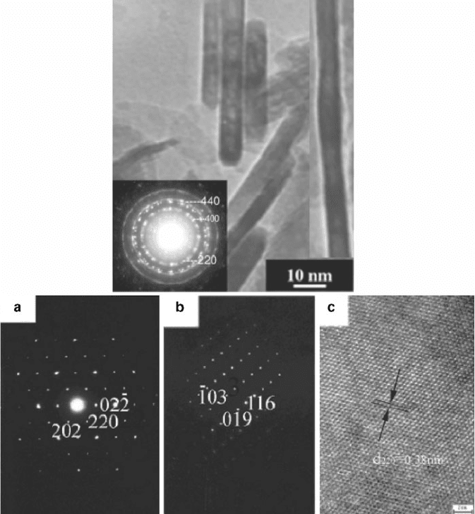
Figure 7.14. (Top) SAED pattern from a polycrystalline MgAl
2
O
4
nanorods.
[30]
(bottom) SAED patterns
(a, b) and high-resolution TEM image (c) of a single-crystalline In
2
S
3
nanoparticle. Images (a) and (b)
illustrate the diffraction patterns for cubic and tetragonal unit cells, respectively. The TEM image
shown in (c) illustrates the lattice fringes and interplanar spacing of 3.81 A
˚
, corresponding to the (220)
interplanar spacing of cubic In
2
S
3
.
[31]
In high-resolution images, lattice fringes result from the
interference of the transmitted and diffracted beams; these are only evident in the TEM image when the
lattice spacings are larger than the resolution of the electron microscope.
604 7 Materials Characterization
the amplificat ion of the incident electron beam via a MCP – resulting in much lower
intensities of the incident ele ctron beam.
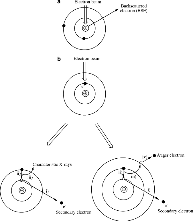
In addition to structural information from crystalline samples, quantitative analy-
sis may also be carried out in tandem with TEM (and SEM) analyses. The interaction
among high-energy electrons and sample atoms results in a variety of emissions
(Figure 7.15) that yield important information regarding the surface morphology and
elemental composition of the sample. As previously stated, if the electron beam
Figure 7.15. Types of possible interactions between the primary electron beam and (a) the nucleus of
surface atoms and (b) electrons of surface atoms comprising the sample. For simplicity, only K, L, and M
shells (with no L and M subshells) are shown.
7.2. Electron Micros copy 605
interacts with the nucleus of surface atoms, the electrons are elastically scattered. In
this case, the trajectory of the electron changes with no change in the kinetic energy
or velocity, a process known as backscattering.
The number of backscattered electrons (BSE) that are p roduced from a given
atom is proportional to the atomic number. That is, materials composed of heavy
atoms will backscatter more electrons, resulting in brighter gray tones in the image
relative to less dense materials. Hence, BSE produce an image that is related to
material composition, providing both spatial and chemical information. Accord-
ingly, it is often easier to accurately determine the sizes/spatial positions of high- Z
nanoparticles via so-called dark-field imaging relative to bright-field imaging, which
is more easily shaded by the varying contrast of the support material (Figure 7.16).
The primary electron beam may also be inelastically scattered through interaction
with electrons from surface atoms. In this case, the collision displaces core electrons
from filled shells (e.g., ns
2
(K) or np
6
(L)); the resulting atom is left as an energetic
excited state, with a missing inner shell electron. Since the energies of these secondary
electrons are sufficiently low, they must be released from atoms near the surface
in order to be detected. Electrons ejected from further within the sample are reab-
sorbed by the material before they reach the surface. As we will see in the next section
(re SEM), as the intensity of the electron beam increases, or the density of the sample
decreases, information from underlying portions of the sample may be obtained.
In order for the excited-stat e atom to return to its ground state (within a picosec-
ond or so following secondary electron generation), the vacancy in the K shell is
filled with an electron from shells farther from the nucleus (e.g., L shell, Figure 7.17 ).
When such post-ionization atomic relaxation occurs, the excess energy may be
released as either characteristic X-rays, or through nonradiative emission of an
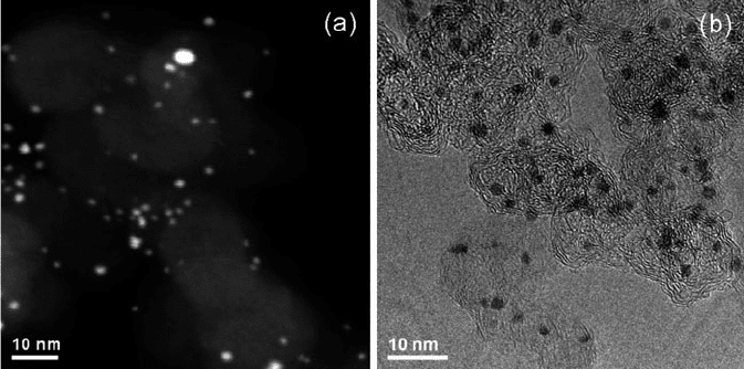
Figure 7.16. Dark-field (a), and bright-field (b) TEM images of Pt nanoparticles supported on carbon
(Vulcan XC-72). Reproduced with permission from Langmuir 2008, 24, 11350. Copyright 2008 American
Chemical Society.
606 7 Materials Characterization
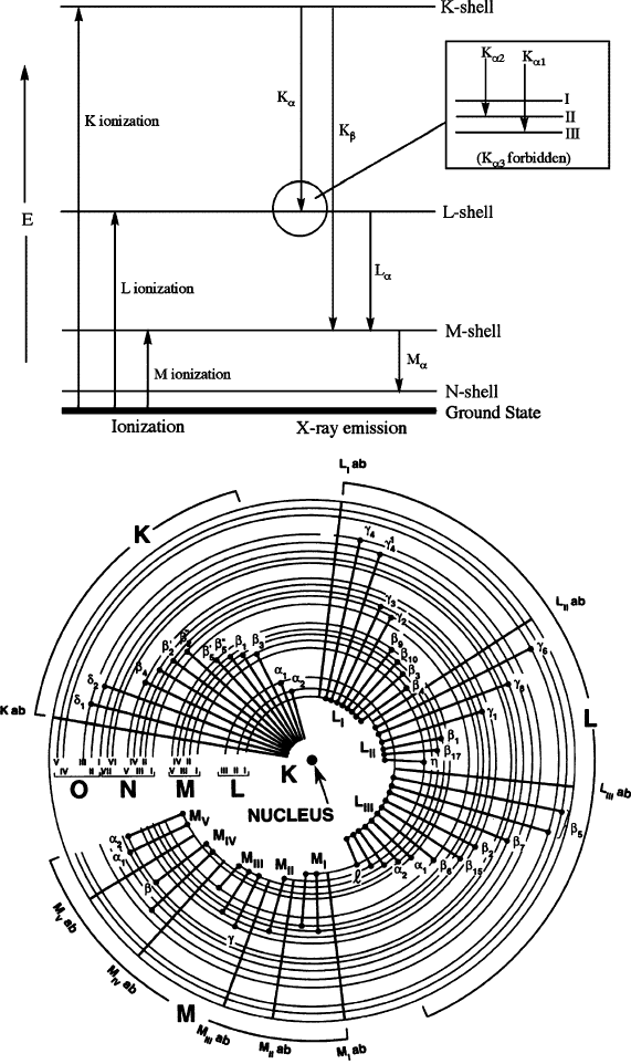
Figure 7.17. Simplified (top) and detailed (bottom) illustration of atomic energy levels, showing the
characteristic X-rays emitted as the atom’s energy returns to the ground state following ionization. The a
and b designations indicate the filling of K, L, or M electron vacancies from adjacent (n þ 1 ! n) and
(n þ 2 ! n) energy levels, respectively.
[35]
The inset shows transitions between the K shell and L
subshells. The illustration of detailed electronic transitions for Cu was reproduced with permission
from Goldstein, J.; Newbury, D.; Joy, D.; Lyman, C.; Echlin, P.; Lifshin, E.; Sawyer, L.; Michael, J.
Scanning Electron Microscopy and X-Ray Microanalysis, 3rd ed., Kluwer: New York. Copyright 2003
Springer Science and Business Media.
7.2. Electron Micros copy 607