Fahlman B.D. Materials Chemistry
Подождите немного. Документ загружается.

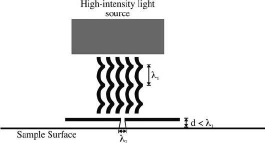
By comparison, the distance between the light source and sample in conventional optical
microscopy is on the order of millimeters. Not unlike other visionary ideas ahead of
their time, the technical difficulties associated with Synge’s idea were only recently
overcome at IBM in the mid-1980s, which marked the rediscovery of the technique
now referred to as near-field scanning optical microscopy (NSOM, Figure 7.2).
[3]
A variety of apertures have been used to deliver nanometer-sized spots of light.
While early NSOM tips were fabricated out of etched quartz crystals and micro-
pipettes, tapered optical fibers with tip diameters of ca. 100 nm are now typically
used. A metallic thin film such as aluminum is usually applied around the sides of
the tapered region of the NSOM tip to focus the light toward the sample. For optical
fibers, the numerical aperture is related to the difference in the indices of refraction
of the cladding and core (Eq. 2):
NA /
ffiffiffiffiffiffiffiffiffiffiffiffiffiffiffiffiffiffiffiffiffiffiffiffiffiffiffiffiffiffiffiffiffiffiffiffiffiffiffiffi
ð
core
Þ
2
ð
cladding
Þ
2
q
ð2Þ
In order to obtain high-resolution optical images with NSOM, the tip must be
stabilized within a few nanometers of the sample surface during scanning. Techni-
ques to precisely position the tip above the sample were developed by researchers in
1992, resulting in more applications for both imaging and topographic profiling of
surfaces. This latter capab ility will be discussed in more detail later in this chapter
when discussing scanning probe microscopy (SPM).
7.2. ELECTRON MICROSCOPY
Although optical microscopy may be extended into the nanoregime, other techni-
ques must be used to clearly discern components below 100 nm. Indeed, the current
“nanotechnology revolution” that we are experiencing would not have been possible
Figure 7.2. Schematic of operating principle of near-field scanning optical microscopy (NSOM).
The resulting wavelength of light impinging on the sample (l
2
) has a wavelength much smaller than
the illuminating source, resulting in much higher resolution.
588 7 Materials Characterization
if there were not suitable techniques in order to characterize nanomaterials. As
we saw in the previous sectio n, in order to improve resolution, we must use source
radiation with as small a wavelength as possible.
Louis DeBroglie was the first to assert that matter, like light, could be described
as having both particle and wave characteristics (Eq. 3). Howeve r, the application
of this equation for a macroscopic item such as a golf ball in flight
[4]
predicts a
wavelength that is too small to be meaningful (Eq. 4). By comparison, subatomic
particles have wavelengths comparable to the size of an atom. In particular, elec-
trons that are accelerated in a potential, V, have quantifiable wav elengths;
[5]
for
example, electrons accelerated at 100 kV have a wavelength of 0.037 A
˚
(Eq. 5). This
is significantly shorter than the wavelengths of high-energy radiation sources such
as X-rays (e.g., 1.54 A
˚
for Cu Ka X-rays), or neutrons (ca. 1 nm). Though neutron
microscopes have recently been demonstrated,
[6]
X-ray microscopes are not possible
due to the lack of suitable refracting lenses for X-rays. However, we will see later
on that X-rays are instrumental for the chemical analysis of a surface.
l ¼
h
mn
ð3Þ
6:626 10
34
Js
ð0:045 kgÞð41 ms
1
Þ
¼ 3:59 10
34
mð4Þ
l¼
12:3A
ffiffiffiffiffiffiffiffiffiffiffiffiffiffiffiffiffiffiffiffiffiffiffi
Vþ
V
2
1 10
6
r
ð5Þ
The ability to focus the extremely sma ll incident wavelengths of energetic
electrons results in an unprecedented spatial resolution compared to optical based
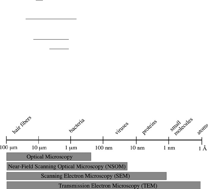
microscopy techniques (Figure 7.3). Since the resolution of our eyes is on the order
of 0.1 mm, in order for us to observe these features, an appropriate level of
magnification must be used. That is, for the increasingly greater resolution capabil-
ities of modern scanning electron microscope (SEM) and transmission electron
Figure 7.3. Comparison of the characterization size regimes for optical and electron microscopy.
7.2. Electron Micros copy 589
microscope (TEM) instruments, the sample must be magnified by ca. 100–300 K
and 1.5–2 M times, respectively (Figure 7.4). However, it should be noted that
although the wavelength of electrons are ca. 100,000 times smaller than visible
light, the resolving power of electron microscopes are only on the order of 1,000
times greater than light microscopes, due to lens aberrations (especially spherical
aberration).
[7]
Images obtained from electron microscopy are due to the nature/degree of
electron scattering from the constituent atoms of the sample. Table 7.1 provides a
comparison betwee n electron, X-ray, and neutron sources, pertaining to their utility
for scattering applications. Electrons are much less penetrating than X-rays, and are
readily absorbed by air, dictating the use of ultrahigh vacuum (UHV) environments.
Since the mass of an electron is 1,000 times smaller than the lightest nucleus,
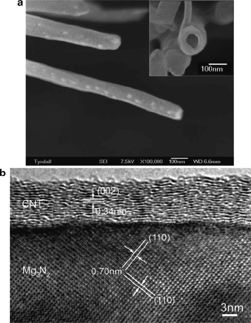
Figure 7.4. High-resolution (HR) electron micrographs. Shown is (a) an SEM image of vanadium oxide
nanotubes at a magnification of 100,000
[8]
and (b) a TEM image of the interface between a Mg
3
N
2
nanowire and a graphitic carbon coating at a magnification of ca. 2,000,000.
[9]
590 7 Materials Characterization
electrons are scattered much more intensely than X-rays or highly penetrating
neutrons. This results in high sensitivity from the interaction of electrons with
constituent atoms of the sample.
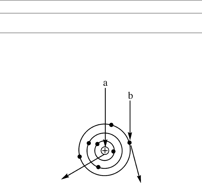
There are two types of scattering interactions that are possible when an electron
beam impinges on atoms of the sample (Figure 7.5). Interaction between the electron
source and atomic nuclei gives rise to elastic scattering , which results in a large-
angle deflection of the electron beam with little or no energy loss. By comparison,
electron–electron interactions between the source and electron clouds of individual
atoms cause small-angle deflections with a significant loss of energy, known as
inelastic scattering. It should be noted that there is a finite probability that the
electrons may continue their original trajectory through the atomic structure without
scattering. In particular, this is commonly observed with molecules containing light
atoms such as H, Li, B, etc. As you would expect, a solid consisting of a high density
of large atoms such as metallic solids would result in shorter elastic mean free paths,
Table 7.1. Comparative Characteristics of Energetic Radiation Sources
Source Brightness
a
(particles
cm
2
eV
1
sr
1
)
Elastic mean
free path
b
(A
˚
)
Absorption
length
c
(A
˚
)
Minimum probe
size
d
(A
˚
)
Neutrons 1 10
24
1 10
8
1 10
9
1 10
7
X-rays 1 10
26
1 10
4
1 10
6
1 10
3
Electrons 1 10
29
1 10
2
1 10
3
1
Data from http://ncem.lbl.gov/team/team_background.htm
a
Related to the number of particles and the range of incident angles that irradiate a sample.
b
Related to the distance a particle travels in a solid before elastically colliding with constituent atoms.
c
Related to the distance a particle travels in a solid before its energy is absorbed through interactions with
constituent atoms and electrons.
d
Related to the minimum diameter of the source that is used to generate the radiation.
Figure 7.5. Schematic of specific interactions between the electron beam and sample atom. Shown are
(a) an elastically scattered electron and (b) an inelastically scattered electron.
7.2. Electron Micros copy 591
and stronger elastic scattering interactions with incident electrons. By comparison,
organic solids such as polyethylene would primarily exhibit inelastic scattering with
an electron source.
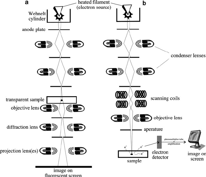
There are two instruments that are used for electron imaging: TEM and SEM. As
the name implies, the transmission mode measures the intensity from an electron
source after it has passed through a transparent sample (Figure 7.6a). In contrast,
SEM features the scanning of an electron beam over selected regions of an opaque
sample (Figure 7.6b).
The basic principles that govern electron microscopy are analogous to optical
microscopy. Whereas optical microscopes use light and optical lenses to illuminate
and magnify the sample, electron microscopes utilize high-energy electrons and
Figure 7.6. Schematic of the major components of (a) transmission electron microscope (TEM) and
(b) scanning electron microscope (SEM). Note: stigmator coils are also associated with the lens(es) that
reduce beam astigmatism, thereby improving image distortion and resolution. For TEM, the image is shown
to be projected onto a viewing screen. This screen is coated with phosphorescent particles such as ZnS
and CdS that emit visible light when struck by electrons (hard copies of the image may also be transferred
to photographic plates via silver halide emulsions). However, modern TEM instruments do not require
photographic development, as digital images are observed directly on computer monitors, in real time.
592 7 Materials Characterization
electromagnetic lenses (i.e., magnetic coils). There are two types of lenses in
electron microscopes (see below); TEM has an additional lens, the projector lens,
which is used to project an amplified copy of the image onto a screen:
(i) Condenser – used to control the illumination of the sample by concentrating the
electron beam generated from the source.
(ii) Objective – used to magnify and focus the image formed from electrons inter-
acting with the sample (in TEM, the sample is inserted into the objective lens).
(iii) Projector – used to project an amplified copy of the image onto a screen
(photographic plate, computer screen, fluorescent screen, CCD camera/
monitor).
7.2.1. Electron Sources
The heart of any electron microscope is the electron source, or gun. In fact, the
electron gun within microscopes is identical to that operating within mode rn tele-
visions. Behind the TV monitor is a cathode ray tube (CRT), which contains a set of
three tungsten filaments. The electrons generated from these filaments are acceler-
ated toward an anode that is coated with phosphor particles, which emit either red,
green, or blue light when struck with electrons. This light is focused onto individual
pixels that comprise the monitor; if you look close at a television screen, you may
notice the millions of tiny dots that comprise individual images. The picture we see
on our monitors is a result of the electron guns being scanned sequentially from left
to right in a fraction of a second, a process known as rastering. This is the exact
mode that is operable in SEMs and scanning transmission electron microscopes
(STEM), where the focused electron beam is allowed to scan across selected regions
of a sample.
Electrons are generated by passing high currents through tungsten or crystalline
LaB
6
(or CeB
6
) filaments, resulting in temperatures on the order of 2,700–2,900 K or
1,500 K, respectively. The thermal release of electrons at the Fermi level of the
material is known as thermionic emission, and may only occur once the energy
exceeds the work function of the material (4.7 and 2.7 eV for W and LaB
6
,
respectively). Saturation of the filament occurs when further heating does not
increase the number electrons being emitted. Electrons ejected from the filament
cathode are focused by a negat ively charged Wehnelt cylinder, and drawn toward a
positively charged anode plate containing a small aperture (Figure 7.6). The elec-
trons that escape through the pinhole are directed down the column toward the
sample. The voltage difference between the filament and the anode plate is referred
to as the accelerating voltage. This value is directly proportional to the energy of the
electron beam that is directed down the colu mn. Whereas the voltage range for SEM
is ca. 200 V–40 kV, TEMs feature much higher accelerating voltages, ranging from
60 to 400 kV. All electron microscopes must be operated under extremely high
vacuum conditions (ca.10
6
–10
9
Torr), which provides an insulating medium
between the cathode and anode, prolongs the lifeti me and efficiency of the gun, and
allows for sharper beam focusing. In general, the characteristics of an electron gun
7.2. Electron Micros copy 593
may be optimized by varying four components: the distance from the filament to the
opening of the Wehnelt cylinder, the temperature of the filament, the negative bias
of the Wehnelt cylinder with respect to the cathode, and the brightness of the beam.
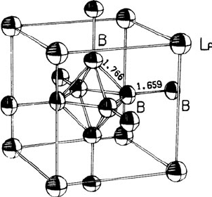
Lanthanum hexaboride crystal filaments yield a brightness ca. 10 times greater
than W, with a smaller spot size. This allows for imaging at very low accelerating
voltages without a loss of resolution – of importance for beam-sensitive samples. Due
to the small spot size, the beam from a LaB
6
source is highly monochromatic, which
increases the overall resolution (i.e., less chromatic aberrations). Interestingly, LaB
6
filaments employ the (100) face due to its relatively low work function.
[10]
The
preferential release of electrons from this crystal face is likely due to the dipole
existing between the positively charged metal atoms at the crystal surface, and
the underlying layer of boride octahedra (Figure 7.7). A high vacuum must be used
to prevent oxidation of the crystal surface; adsorption of oxygen raises the work
function of LaB
6
from 2.70 – 4.0 eV.
[11]
It should be noted that the work function of structural alloys is always less than the
work function of the isolated component metals. For instance, the work functions of
B and La are 4.5 and 3.3 eV, respectively – much higher than LaB
6
. The mechanisms
responsible for the reduction of the work function are not completely understood,
although it must depend on the three-dimens ional arrangement and orbital overlap of
electron rich/deficient atoms or ions near the surface of the solid. Once this mecha-
nism is deciphered, many more materials will be isolated as effective candidates for
electron emission sources.
In order to increase the intensity and focus of electrons, a field emission source
may be used. This consists of a single crystal tungsten or LaB
6
(100) wire that is
sharpened to a tip diameter of ca. 100 nm–1 mm. For crystalline tungsten, the axis is
suitably aligned with respect to the optical axis of the microscope. For example, a
beam with a diameter < 5 nm is possible from alignment of the filament planes
Figure 7.7. Unit cell of LaB
6
. Thermal vibration ellipsoids are also shown, illustrating a significant
anisotropy in the thermal vibrations of the B atoms. Reproduced with permission from Lundstrom, T.
Pure Appl. Chem. 1985, 57, 1383. Copyright 1985 IUPAC.
594 7 Materials Characterization

perpendicular to h310i and h111i. In addition to W and LaB
6
, a number of other
materials are proposed for field emission applications, such as silicon, single-walled
nanotubes,
[12]
and ultrananocrystalline diamond (UNCD) or Cu/Li alloy films
deposited onto sharpened tips.
[13]
Two classifications of field emitters are used in electron microscopes, cold and
Schottky sources (Table 7.2). Whereas the former operates through Fowler-Nord-
heim electron tunneling
[14]
from a cathode wire held at room temperature, the latter
features thermionic emission from a ZrO
2
-coated sharpened W filament at 1,800 K.
In both cases, an electrical field draws electrons from the narrow filament tip into an
ultrahigh vacuum (10
9
Pa) chamber. When the electrons are accelerated through
the magnetic field and focused onto the sample, a dramatically greater resolution is
obtained – ca. 15 times that of traditional filaments (Figure 7.8 ). The magnification,
M and resolution R, are given by Eqs. 6 and 7:
[15]
M=
L
r
;ð6Þ
where: L ¼ distance from the tip to the screen/detector
r ¼ radius of the tip apex
R=
M
t
;ð7Þ
where: M ¼ magnification
t ¼ time-of-flig ht of an electron from tip to the screen/detector
Though cold FE sources feature a higher brightness and smaller spot size than a
Schottky FE source, they are not as preferred due to their relat ively noisy emission
profile. This beam instability arises from the Brownian motion of adsorbed residual
gases on the surface of the narrow tip. Though electron microscopes are operated
Table 7.2. Comparison of Various Electron Sources
[16]
Thermionic
W
Thermionic
LaB
6
Cold FE
W(310)
Schottky FE
ZrO/W(100)
Operating temperature (K) 2,800 1,900 300 1,800
Operating vacuum (kPa) 1 10
5
1 10
6
1 10
10
1 10
8
Cathode radius (nm) 60,000 10,000 100 1,000
Effective source radius (nm) 15,000 5,000 2.5 15
Emission current density (A cm
2
) 3 30 17,000 5,300
Total emission current (mA) 200 80 5 200
Normalized brightness
(A cm
2
sr
1
kV
1
)
1 10
4
1 10
5
2 10
7
1 10
7
Maximum probe current (nA) 1,000 1,000 0.2 20
Energy spread at the cathode (eV) 0.59 0.40 0.26 0.31
Energy spread at the gun exit (eV) 1.5–2.5 1.3–2.5 0.3–0.7 0.35–0.71
Beam noise (%) 1 1 5–10 1
Emission current drift (% h
1
) 0.1 0.2 5 <0.5
Cathode lifetime (h) 200 >500 >2,000 >2,000
Cathode regeneration Not required Not required Every 6–8 h Not required
Sensitivity to external influences Minimal Minimal High Low
7.2. Electron Micros copy 595
under UHV, these gases are always present in the column – likely originating from
the sample itself (residual solvent on grid, e-beam decomposition of the sample,
etc.). In addition, as electrons strike residual gas molecules in the column, positive
ions are generated that may be accelerated back to the electron source. Such ion
bombardment will cause a significant deformation of the filament surface, which
will lead to beam instabilities. Since Schottky emitters are operated at 1,800 K, these
deformations are readily repaired via annealing. Howeve r, this is not possible using
cold FE sources, which must be periodically “flashed” with a high-temperature pulse
in order to repair surf ace deformations. Though this effectively improves the surface
structure of the emitter, the lifetime of the emitter is shorted due to an increase in the
tip radius – a consequence of thermal flashing in the absence of an electric field.
Figure 7.8. Comparison of the resolution for (a) low-resolution SEM,
[17]
with (b) high-resolution
FESEM.
[18]
Both images are of a nanoporous anodized aluminum oxide template at identical magnification.
596 7 Materials Characterization
7.2.2. Transmission Electron Microscopy (TEM)
A transmission electron microscope is analogous to a slide projector, with illumina-
tion from an electron beam rather than light. When an electron beam is imping ed
upon a sam ple, a black and white TEM image is formed from the passage of some
electrons through the sample untouched, alon gside the combination of interactions
between other electrons and sample atoms (e.g., inelastic/elastic scattering, diffrac-
tion). If the undiffracted beam is selected to form the image, it is referred to as
bright-field imaging; in contrast, selection of strongly diffracting regions of the
sample, which would appear brighter than the transmitted beam, is known as
dark-field imaging.
[19]
It should be noted that electrons may also be absorbed by
molecules containing large atoms, or by surface contamination (e.g., dust, grease).
The absorption of a high density of electrons in a specific region will cause a buildup
of heat, leading to sample destruc tion and poor image quality.
Analogous to throwing a baseball of varying speeds through a wall, the relative
degree of penetration through a particular sample is governed by the energy of the
electron source. That is, higher energy electrons (e.g., 200 keV vs. 100 keV) will be
more penetrating, allowing for the characterization of thicker and/or less transparent
samples. In general, increasing the thickness of a sample, or decreasing the energy
(i.e., accelerating voltage) of the electron beam, will induce more scattering events
through more effective interactions between the electron beam and atoms of the
sample. This effect will enhance image contrast, since there is a larger deviation
between the path lengths of transmitted and scattered electrons that reach the
viewing screen. However, this improvement of image quality is offset by plentiful
inelastic collisions that yield a broadened wavelength distribution of the electron
beam. Since individual electrons will have differing energies, they will be brought
into focus at different points resulting in a blurry image (i.e., decreased resolution).
Sample preparation techniques
Not unlike other materials (or molecular) characterization techniques, the most
important and time-consuming aspect of TEM analysis is sample preparation.
Specimens for TEM analysis are placed on special micromesh grids of a conductive
metal such as Cu, Au, or Ni. The typical dimensions of TEM grids are ca. 3 mm in
diameter and 10–25 mm thick. The mesh number of a grid indicates the number of
grid openings per linear inch. The smaller the grid number, the larger the hole size
and the greater the ratio of open area to covered area (Figure 7.9a). For example, a
200-mesh grid has 20 holes along its diameter; a 400-mesh grid has 40 holes.
This translates to hole sizes of ca. 200 mm for 100-mesh, ca.97mm for 200 mesh,
ca.63mm for 300 mesh, and ca.42mm for 400-mesh grids.
Most often, a grid is coated with a support film that holds the sample in place. The
film must be as transparent as possible, while providing support for the sample. To
prevent interference with electron-sample interactions, films containing light elements
(e.g., C, Be) are used. Support films are typically deposited onto the surface of grids
through a “floating” technique (Figure 7.9b). Amorphous carbon or polymeric
7.2. Electron Micros copy 597