Bhushan B. Nanotribology and Nanomechanics: An Introduction
Подождите немного. Документ загружается.

374 Bharat Bhushan
a) b)
c)
Normal load (μN)
Distance (μm)
025
125
100
75
50
25
0
2.5
2.0
1.5
1.0
0.5
0.0
5
10 15 20
Friction signal (V)
Coefficient of friction
Normal load (μN)
0
125
0.5
0.4
0.3
0.2
0.1
0.0
25
50 75 100
0 nm 20 nm
2 μm
Si(100)
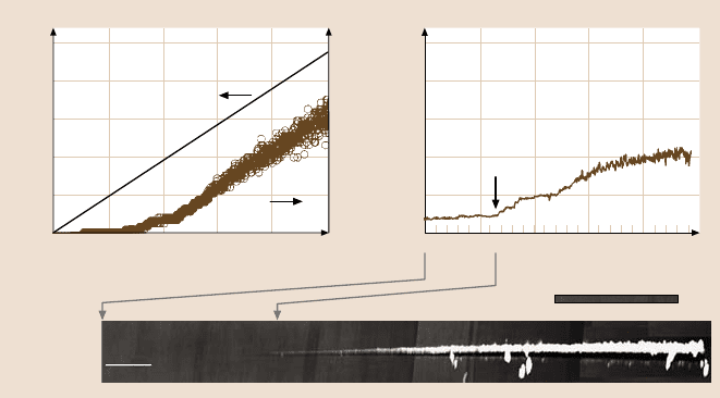
Fig. 8.45. (a) Applied normal load and friction signal measured during the microscratch ex-
periment on Si(100) as a function of scratch distance, (b) friction data plotted in the form
of coefficient of friction as a function of normal load, and (c) AFM surface height image of
scratch obtained in tapping mode [47]
Scratching can be performed under ramped loading to determine the scratch
resistance of materials and coatings. The coefficient of friction is measured dur-
ing scratching and the load at which the coefficient of friction increases rapidly is
known as the critical load, which is a measure of scratch resistance. In addition,
post-scratch imaging can be performed in situ with the AFM in tapping mode to
study failure mechanisms. Figure 8.45 shows data from a scratch test on Si(100)
with a scratch length of 25µm and a scratching velocity of 0.5µm/s. At the begin-
ning of the scratch, the coefficient of friction is 0.04, which indicates a typical value
for silicon. At about 35 µN (indicated by the arrow in the figure), there is a sharp
increase in the coefficient of friction, which indicates the critical load. Beyond the
critical load, the coefficient of friction continues to increase steadily. In the post-
scratch image, we note that at the critical load a clear groove starts to form. This
implies that Si(100) was damaged by plowing at the critical load, associated with
the plastic flow of the material. At and after the critical load, small and uniform
debris is observed and the amount of debris increases with increasing normal load.
SundararajanandBhushan[47] havealso used thistechniqueto measurethe scratch
resistance of diamond-like-carboncoatings with thicknesses of 3.5–20 nm.
8.4.3 Microscale Wear
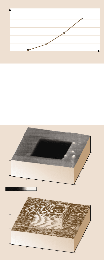
By scanning the sample in two dimensions with the AFM, wear scars are generated
on the surface. Figure 8.46 shows the effect of normal load on wear depth. We note
that wear depth is very small below 20 µN of normal load [118, 119]. A normal
8 Nanotribology, Nanomechanics and Materials Characterization 375
Wear depth (nm)
Normal load (μN)
0
100
125
100
75
50
25
0
20 40 60 80
Fig. 8.46. Wear depth as
a function of normal load for
Si(100) after one cycle [119]
load of 20 µN corresponds to contact stresses comparable to the hardness of the
silicon. Primarily, elastic deformation at loads below 20µN is responsible for low
wear [28,29].
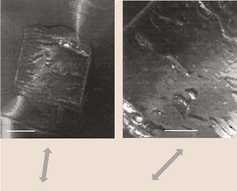
A typical wear mark, of the size 2 µm×2µm, generated at a normal load of
40µN for one scan cycle and imaged using AFM with a scan size of 4 µm×4 µmat
300nN load, is shown in Fig. 8.47a [118]. The inverted map of wear marks shown
in Fig. 8.47b indicates the uniform material removalat thebottom of the wear mark.
4.00
0
0
1.00
2.00
3.00
4.00 μm
50.0
100
nm
3.00
2.00
1.00
0
4.00
0
0
1.00
2.00
3.00
4.00 μm
50.0
100
nm
3.00
2.00
1.00
0
W = 40μN
d = 30 nm
1 Cycle
a)
0.0 50.0 nm25.0
b)
Fig. 8.47. (a) Typical
greyscale and (b)inverted
AFM images of wear mark
created using a diamond tip
at a normal load of 40 µNand
one scan cycle on a Si(100)
surface
376 Bharat Bhushan
Tip sliding direction
1 μm
40 μN
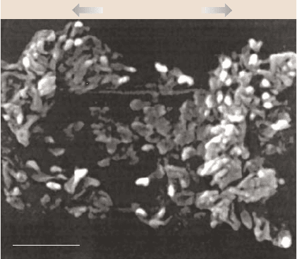
Fig. 8.48. Secondary electron
image of wear mark and
debris for Si(100) produced
at a normal load of 40 µNand
one scan cycle
An AFM image of the wear mark shows small debris at the edges, swiped during
AFM scanning. Thus the debris is loose (not sticky) and can be removed during the
AFM scanning.
Next we examine the mechanism of material removal on a microscale in AFM
wear experiments [30,118,119]. Figure 8.48 shows a secondary-electron image of
the wear mark and associated wear particles. The specimen used for the scanning
electron microscope (SEM) was not scanned with the AFM after initial wear, in
order to retain wear debris in the wear region.Wear debrisis clearly observed.In the
SEM micrographs, the wear debris appears to be agglomerated because of the high
surface energy of the fine particles. Particles appear to be a mixture of rounded and
so-calledcutting type (feather-likeor ribbon-likematerial). Zhaoand Bhushan[119]
reported an increasein the number and size of cutting-typeparticleswith the normal
load. The presence of cutting-type particles indicates that the material is removed
primarily by plastic deformation.
To understand the material removal mechanisms better, transmission electron
microscopy (TEM) has been used. The TEM micrograph of the worn region and
associated diffraction pattern are shown in Fig. 8.49a,b. The bend contours are ob-
served to pass through the wear mark in the micrograph. The bend contours around
and inside the wear mark are indicative of a strain field, which in the absence of
applied stresses can be interpreted as plastic deformation and/or elastic residual
stresses. Often, localized plastic deformation during loading would lead to residual
stresses during unloading; therefore, bend contours reflect a mix of elastic and plas-
tic strains. The wear debris is observedoutside the wear mark.The enlarged view of
the wear debris in Fig. 8.49c shows that much of the debris is ribbon-like, indicat-
ing that material is removed by a cutting process via plastic deformation, which is
consistent with the SEM observations. The diffraction pattern from inside the wear
mark is similar to that of virgin silicon, showing no evidence of any phase trans-
8 Nanotribology, Nanomechanics and Materials Characterization 377
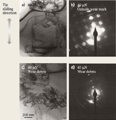
Fig. 8.49. Bright-field TEM micrographs (left) and diffraction patterns (right) of wear mark
(a), (b) and wear debris (c), (d) in Si(100) produced at a normal load of 40 µN and one scan
cycle. Bend contours around and inside wear mark are observed
formation (amorphization) during wear. A selected area diffraction pattern of the
wear debris shows some diffuse rings, which indicates the existence of amorphous
material in the wear debris, confirmed as silicon oxide productsfrom chemical anal-
ysis. It is known that plastic deformation occurs by generation and propagation of
dislocations. No dislocation activity or cracking was observed at 40 µN. However,
dislocation arrays could be observed at 80 µN. Figure 8.50 shows the TEM micro-
graphs of the worn region at 80µN; for better observation of the worn surface, wear
debris was moved out of the wear mark by using AFM with a large-area scan at
300nN after the wear test. The existence of dislocation arrays confirms that mate-
rial removal occursby plastic deformation.This corroboratesthe observationsmade
in scratch tests with a ramped load in the previous section. It is concluded that the
material on the microscale at high loads is removed by plastic deformation with
a small contribution from elastic fracture [119].
To understand wear mechanisms, the evolution of wear can be studied using
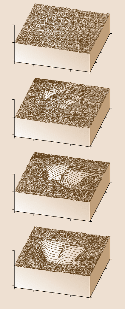
AFM.Figure 8.51showsevolutionof wear marksof a DLC-coateddisk sample.The
data illustrate how the microwear profile for a load of 20 µN develops as a function
of the number of scanning cycles [27]. Wear is not uniform, but is initiated at the
nanoscratches. Surface defects (with high surface energy) present at nanoscratches
act as initiation sites for wear. Coating deposition may also not be uniform on and
378 Bharat Bhushan
Tip
sliding
direction
1 μ
m
200
nm
a)
b)
Tip
sliding
direction
80 μN
80 μN
Fig. 8.50. (a) Bright-field and (b) weak-beam TEM micrographs of wear mark in Si(100)
produced at a normal load of 80 µN and one scan cycle showing bend contours and disloca-
tions [119]
near nanoscratches,which may lead to coating delamination.Thus, scratch-freesur-
faces will be relatively resistant to wear.
Wear precursors (precursors to measurable wear) can be studied by making sur-
face potential measurements [66–68]. The contact potential difference or simply the
surface potential between two surfaces depends on a variety of parameters such as
the electronic work function, adsorption, and oxide layers. The surface potential
map of an interface gives a measure of changes in the work function which,is sensi-
tive to bothphysical andchemical conditionsof the surfacesincluding structuraland
chemical changes. Before material is actually removed in a wear process, the sur-
face experiences stresses that result in surface and subsurface changes of structure
and/or chemistry. These can cause changes in the measured potential of a surface.
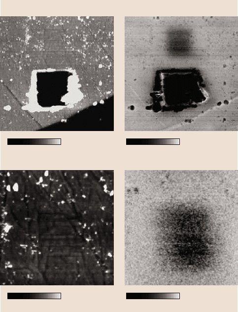
An AFM tip allows mapping of surface potential with nanoscale resolution. Surface
height and change in surface potential maps of a polished single-crystal aluminum
(100) sample abraded using a diamond tip at loads of 1 µNand9µN, are shown in
Fig. 8.52a[Note that the signof the change in surfacepotentialis reversedhere from
that in DeVecchio and Bhushan [66]]. It is evident that both abraded regions show
a large potential contrast (≈0.17V), with respect to the non-abradedarea. The black
region in the lower right-hand part of the topography scan shows a step that was
created during the polishing phase. There is no potential contrast between the high
regionand the lowregion of the sample,indicating that the techniqueis independent
of surface height. Figure 8.52b shows a close-up scan of the upper (low-load) wear
region in Fig. 8.52a. Notice that, while there is no detectable change in the surface
topography, there is nonetheless a large change in the potential of the surface in the
8 Nanotribology, Nanomechanics and Materials Characterization 379
4.00
0
0
1.00
2.00
3.00
4.00 μm
500
1000
nm
3.00
2.00
1.00
0
20 μN
10 cycles
4.00
0
0
1.00
2.00
3.00
4.00 μm
500
1000
nm
3.00
2.00
1.00
0
20 μN
15 cycles
4.00
0
0
1.00
2.00
3.00
4.00 μm
500
1000
nm
3.00
2.00
1.00
0
4.00
0
0
1.00
2.00
3.00
4.00 μm
500
1000
nm
3.00
2.00
1.00
0
20 μN
5 cycles
20 μN
20 cycles
Fig. 8.51. Surface plots of
diamond-like carbon-coated
thin-film disk showing the
worn region; the normal load
and number of test cycles are
indicated [27]
380 Bharat Bhushan
worn region. Indeed, the wear mark of Fig. 8.52b might not be visible at all in the
topography map were it not for the noted absence of wear debris generated nearby
and then swept off during the low-load scan. Thus, even in the case of zero wear
(no measurable deformation of the surface using AFM), there can be a significant
change in the surface potential inside the wear mark, which is useful for the study
of wear precursors. It is believed that the removal of the thin contaminant layer in-
cluding the natural oxide layer gives rise to the initial change in surface potential.
The structural changes, which precede generation of wear debris and/or measurable
wear scars, occur under ultra-low loads in the top few nanometers of the sample,
and are primarily responsible for the subsequent changes in surface potential.
Surface height Surface potential
10 μm 10 μm
0 200 mV0 100 nm
5 μm5 μm
0 150 mV0 25 nm
a)a)
b)
Fig. 8.52. (a) Surface height and change in surface potential maps of wear regions generated
at 1 µN(top)and9µN(bottom) on a single-crystal aluminum sample showing bright contrast
in the surface potential map on the worn regions. (b) Close-up of upper (low-load) wear
region [66]
8 Nanotribology, Nanomechanics and Materials Characterization 381
8.4.4 In Situ Characterization of Local Deformation
In situ surface characterization of local deformation of materials and thin films is
carried out using a tensile stage inside an AFM. Failure mechanisms of polymeric
thin films under tensile load were studied by Bobji and Bhushan [61,62]. The spec-
imens were strained at a rate of 4×10
−3
% per second and AFM images were cap-
tured at different strains up to about 10% to monitor generation and propagation of
cracks and deformation bands.
Bobji and Bhushan [61,62] studied three magnetic tapes with thickness ranging
from 7 to 8.5µm. One of these was with acicular-shaped metal particle (MP) coat-
ing and the other two with metal-evaporated (ME) coating and with and without
a thin diamond-like carbon (DLC) overcoat both on a polymeric substrate and all
with particulate back-coating [15]. They also studied a polyethylene terephthalate
(PET) substrate with a thickness of 6 µm. They reported that cracking of the coat-
ings started at about 1% strain for all tapes, well before the substrate starts to yield
Strain
0.83%
Loading
direction
1.88%
2.75%
3.75%
5.06%
6.10%
30
nm
15
0
1μm
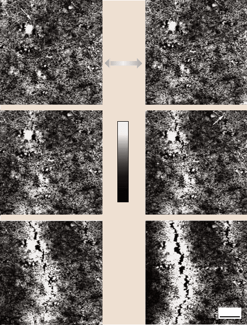
Fig. 8.53. Topographical images of the MP magnetic tape at different strains [61]
382 Bharat Bhushan
at about 2% strain. Figure 8.53 shows the topographical images of the MP tape at
different strains. At 0.83% strain, a crack can be seen, originating at the marked
point. As the tape is further stretched along the direction, as shown in Fig. 8.53, the
crack propagatesalong the shorter boundaryof the ellipsoidal particle. However,the
general direction of the crack propagation remains perpendicular to the direction of
the stretching.The length, width, and depth of the cracks increase with strain, and at
the same time newer cracks keep on nucleating and propagating with reduced crack
spacing. At 3.75% strain, another crack can be seen nucleating. This crack contin-
ues to grow parallel to the first one. When the tape is unloaded after stretching up to
a strain of about 2%, i.e. within the elastic limit of the substrate, the cracks rejoin
perfectly and it is impossible to determine the difference from the unstrained tape.
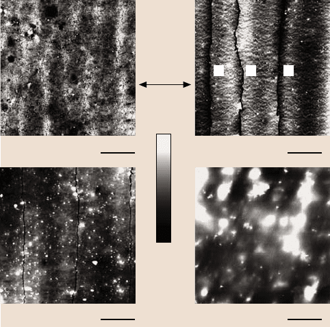
Figure 8.54 shows topographical images of the three magnetic tapes and the
PET substrate after being strained to 3.75%, which is well beyond the elastic limit
of the substrate. MP tape develops numerous short cracks perpendicular to the di-
rection of loading. In tapes with metallic coating, the cracks extend throughout the
tape width. In ME tape with DLC coating, there is a bulge in the coating around the
primary cracks that are initiated when the substrate is still elastic, like crack A in the
figure. The white band on the right-hand side of the figure is the bulge of another
crack. The secondary cracks, such as B and C, are generated at higher strains and
are straighter compared to the primary cracks. In ME tape which has a Co−Ofilm
30
nm
15
0
Strain
3.75%
Loading
direction
MP tape
5 μm ME tape 5 μm
ME without DLC
5 μm PET front side 5 μm
A
C B
Fig. 8.54. Comparison of crack morphologies at 3.75% strain in three magnetic tapes and
PET substrate. Cracks B and C, nucleated at higher strains, are more linear than crack A [62]
8 Nanotribology, Nanomechanics and Materials Characterization 383
on a PET substrate, with a thickness ratio of 0.03, both with and without DLC coat-
ing, no difference is observed in the rate of growth between primary and secondary
cracks. The failure is cohesive with no bulging of the coating. This seems to suggest
that the DLC coating has residual stresses that relax when the coating cracks, caus-
ing delamination. Since the stresses are already relaxed, the secondary crack does
not result in delamination. The presence of the residual stress is confirmed by the
fact that a free-standing ME tape curls up (in a cylindrical form with its axis per-
pendicular to the tape length) with a radius of curvature of about 6mm and the ME
tape without the DLC does not curl. The magnetic coating side of the PET substrate
is much smoother at shorter scan lengths. However, in 20µm scans it has a lot of
bulging out, which appears as white spots in the figure. These spots change shape
even while scanning the samples in tapping mode at very low contact forces.
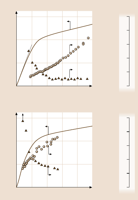
Width
Spacing
Stress
(MPa)
Strain (%)
010
150
100
50
0
0.6
0.4
0.2
0.0
2468
Crack width
(μm)
MP tape
25
20
15
10
5
0
Stress
(MPa)
Strain (%)
010
150
100
50
0
0.6
0.4
0.2
0.0
2468
ME tape
25
20
15
10
5
0
Crack width
(μm)
Crack spacing
(μm)
(67)
Width
Spacing
Crack spacing
(μm)
Fig. 8.55. Variation of stress, crack width, and crack spacing with strain in two magnetic
tapes [61]