Bhushan B. Nanotribology and Nanomechanics: An Introduction
Подождите немного. Документ загружается.

1274 Bharat Bhushan
Torsion hinge
Mirror
Mirror array
Yoke and
hinge array
Metal array
AFM images
of various
arrays
Yoke
Via 2 contact
to CMOS
Landing site
CMOS
memory
Spring tip
Mirror
address
electrode
Yoke
address
electrode
Bias reset bus
DMD exploded pixel view
14 μm
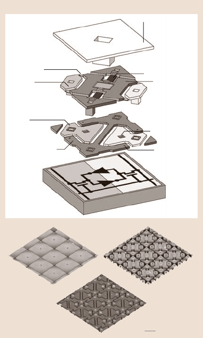
Fig. 22.53. Exploded view
of a DMD pixel and AFM
surface-height images of
various arrays. The DMD
layers were removed by an
ultrasonic method [192]
tion of micromirrors; these are also sometimes used for the construction of hinges,
spring tips, and landing sites. The aluminium alloy films are overwhelmingly com-
prised of aluminium; trace elements (including Ti and Si) are present to suppress
contact spiking and electromigration, which may occur if current densities become
high during electrostatic operation. Multilayered sputtered SiO
2
TiN/Al alloy films
are now generallyused for the landingsite structure to minimize refractionthrough-
out the visible region of the electromagnetic spectrum in order to increase the con-
trast ratio in projection display systems [193, 194]. These multilayered films are
also generally used for hinges and spring tips. A low-surface-energy SAM is main-
tained on the surfaces of the DMD, which is packaged in a hermetic environment
to minimize stiction during contact between the spring tip and the landing site. An
SAM of perfluorinated n-alkanoic acid (C
n
F
2n−1
O
2
H) (e.g., perflurordecanoic acid
or PFDA, CF
3
(CF
2
)
8
COOH) applied by the vapor-phase deposition process is used.
A getter strip of PFDA is included inside the hermetically sealed enclosure contain-
22 Characterization of MEMS/NEMS and BioMEMS/BioNEMS 1275
ing the chip, which acts as a reservoir in order to maintain a PFDA vapor within
the package.
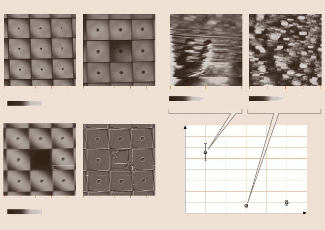
In order to identify a stuck mirror and characterize its nanotribological proper-
ties, the chip was scanned using an AFM [192]). It was found that it is hard to tilt
the stuck micromirror back to its normal position by adding a normal load at the
rotatablecorner of the micromirror;thus, this is called a hard stuck micromirror. An
exampleof a stuck micromirroris shownin Fig. 22.54a.Once the stuck micromirror
was found, the region was repeatedly scanned at a large normal load, up to 300nN.
After severalscans, thestuck micromirrorwasremoved.Once the stuckmicromirror
was removed, the surrounding micromirrors could also be removed by continuous
scanning under a large normal load (Fig. 22.54a bottom row). The adhesive force of
the landing site underneath the stuck micromirror and the normal micromirror are
presented in Fig. 22.54b, which clearly indicates that the landing site underneath
the stuck micromirrorhas much larger adhesion. A 1 µm×1 µm view of the landing
sites under stuck and normal micromirrors are also shown in Fig. 22.54b. The land-
Normal mirrors
40.0
μm
30.020.010.00
Stuck mirror (in the middle)
40.0
μm
30.020.010.00
0 2000 nm
Stuck mirror removed by AFM
40.0
μm
30.020.010.00
Highpass filtered image
40.0
μm
30.020.010.00
0 5000 nm
1.000.750.500.250
0 100 nm
1.000.750.500.250
0 50 nm
Adhesive force (nN)
Landing site
0
Normal II
200
150
100
50
0
Normal IStuck
a) b)
Fig. 22.54. (a)Thetop row shows AFM surface-height images of a stuck micromirror sur-
rounded by eight normal micromirrors. The left image in the bottom row shows the stuck
micromirror, which was removed by an AFM tip after repeated scanning at high normal
load. The right image in the bottom row presents a high-pass-filtered image showing that the
residual hinge that sits underneath the removed micromirror is clearly observed. (b)AFM
surface-height images and adhesive forces of the landing sites underneath the two normal
micromirrors and the stuck micromirror [192]

1276 Bharat Bhushan
ing site under the stuck micromirror has an apparent U-shaped wear mark, which is
surrounded by a smeared area.
Liu and Bhushan[192] calculatedcontact stresses to examineif the stresses were
high enough to cause wear at the spring tip–landing site interface. The calculated
contact stress value was about 33MPa which is substantially lower than the hard-
ness, therefore much plastic deformation and consequently wear was not expected.
The wear mark was only found on a very few landing sites on the DMD, which
means that the SAM coating can generally endure such high contact stresses. Based
on data reported in the literature, the coverage of vapor-depositedSAMs is expected
to be about 97%. The bond strength of the molecules close to the boundary of the
uncovered sites is expected to be weak. Thus, the uncovered sites and the adjacent
molecules are referred to as defects in the SAM coating. Occasionally, if contact
occurs at the defect sites, the large cyclic stress may be close to the critical load,
and lead to the initial delamination of the SAM coating at the interface. The con-
tinuous contact leads to the formation of a high-surface-energysurface by exposure
of the fresh substrate and the formation of SAM fragments. This eventually leads
to an increase in stiction by the formation of large menisci. Once this happens, the
stress at the contact area is increased, which would accelerate the wear. Based on
this hypothesis, suggested mechanisms for the wear and stiction of the landing site
are summarized in Fig. 22.55. Wear initiates at the defect sites and consequent high
stiction can result in high wear. Improvingthe coverageand wear resistance of SAM
coatings could enhance the yield of DMD.
In some cases, the micromirrors are not fully stuck and can be moved by ap-
plying a load at the rotatable corner of the micromirror with a discontinuous mo-
tion, which is thus called soft stiction. Soft-stuck micromirrors studied by Liu and
Bhushan [195] were identified in quality inspection. These micromirrors encoun-
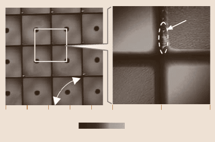
tered slow transition from to end to the other end (+1/ −1). Figure 22.56 shows the
AFM surface-height images of a location showing a stuck mirror (S) and surround-
ing normal micromirrors N
i
(i = 1, 2, and 3). Surprisingly, the images of the stuck
and normal micromirror array are almost the same. On the micromirrors of interest,
a tilting test was performed at the corner of the micromirrors, which are marked by
white dots in Fig. 22.56. The rotatable direction of the microarray is indicated by
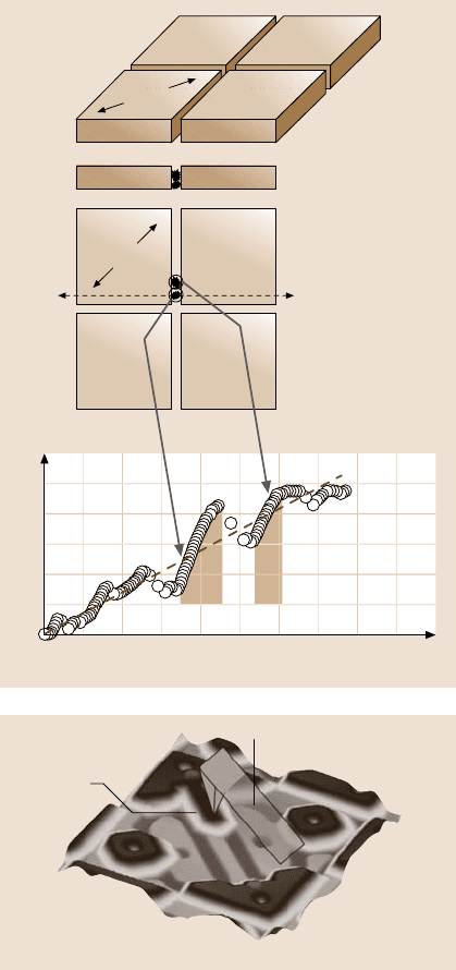
an arrow bar in Fig. 22.56. The load–displacement curve for the stuck micromirror
Defects exist close
to the uncovered sites
Wear could initiate if
contact occurs at uncovered
or defects sites
SAM delaminated
from the interface
Formation of high energy surface
increases the water adsorption,
which in turn leads to large adhesion
Assembled
molecules
Defects
in SAM
Uncovered
sites
Residual
head groups
Molecular
fragments
Water
molecule
Fig. 22.55. Suggested mechanisms for wear and stiction [192]
22 Characterization of MEMS/NEMS and BioMEMS/BioNEMS 1277
40.030.020.010.00 5.02.50
0 1000 nm
N1
N2 N3
S
Fig. 22.56. AFM surface-
height images of normal
micromirrors and a soft-stuck
micromirror. The soft-stuck
micromirror was labeled S,
and the normal micromirrors
studied are labeled as N1, N2,
and N3 [195]
is presented in Fig. 22.57; it is not smooth and appears serrated. It is clearly indi-
cated that, although the S micromirror can be rotated, it rotates with hesitation. In
regimes 1 and 2, as marked in Fig. 22.57, the slopes are much higher. In order to
understandthe mechanismsfor the occurrenceof stiction, stiction of landingsites of
normal and stuck mirrors were measured. Unlike hard-stuck mirrors, the adhesive
forces of soft-stuck and normal mirrors were comparable, which suggests that the
SAM coating is intact with stuck mirror. It was found that a high normalload (about
900nN) and on the order of a couple of hundred scans were required to remove
the soft-stuck micromirrorsby an AFM. However, only about 300nN and about ten
scans were required to remove a hard-stuck mirror. After careful examination of the
AFM images of the micromirror sidewalls in Fig. 22.56 (bottom left), it is noted
that there are contaminant particles attached to the sidewalls of the S mirror. It is,
therefore, believed that, during the tilting test, the S micromirror (see schematic
in Fig. 22.57) a sharper slope regime will occur in the displacement curve. Extra
force is required to overcome the resistance that is induced by the sidewall con-
tamination particles. This is believed to be the reason for the slow transition of the
micromirror during quality inspection.
Finally, the nanomechanical characterization of various layers used in the con-
struction of landing sites, hinge and micromirror materials have been measured by
Wei et al. [193, 194]. Bending and fatigue studies of the hinge have been carried
out by Liu and Bhushan [196] and Bhushan and Liu [197] to measure stiffness
and fatigue properties. For these studies, the micromirror was removed. During re-
moval, the micromirror/yoke structure was removed simultaneously, leaving the
hinge mounted on one end of the array; see Fig. 22.58. The stiffness of the Al hinge
was reported to be comparable to the stiffness of bulk Al. The Al hinge exhibited
a higher modulus than the SiO
2
hinge. The fatigue properties depended upon the
preparation of the hinge for testing.
1278 Bharat Bhushan
Normal load (nN)
Micromirror displacement (nm)
0
0
50
100
150
200 400 1000600 800
3D view
A-A view
Top view
N1 S
N2 N3
N1
N2
S
N3
S rotatable corner
Regime 1 Regime 2
AA
Fig. 22.57. Load–displace-
ment curve obtained on the
rotatable corner of the S mi-
cromirror and schematic to
illustrate the suggested mech-
anism for the occurrence of
soft stiction
AFM cantilever
Hinge
Residual hinge (yoke is removed)
Fig. 22.58. AFM surface-
height image of the residual
hinge and schematic diagram
of the relative position of the
hinge and AFM tip during
the nanoscale bending and
fatigue tests. The tip is lo-
cated at the free end of the
hinge [196]
22.7 Conclusion
The field of MEMS/NEMS has expanded considerably over the last decade. The
length scale and large surface-to-volume ratio of the devices result in very high
retarding forces such as adhesion and friction, which seriously undermine the
performance and reliability of the devices. These tribological phenomena need
22 Characterization of MEMS/NEMS and BioMEMS/BioNEMS 1279
to be studied and understood at the micro- to nanoscales. In addition, materials
for MEMS/NEMS must exhibit good microscale tribological properties. There
is a need to develop lubricants and identify lubrication methods that are suit-
able for MEMS/NEMS. Using AFM-based techniques, researchers have conducted
micro/nanotribologicalstudiesof materialsand lubricantsfor usein MEMS/NEMS.
In addition, component-level testing has also been carried out to aid understanding
of the observed tribological phenomena in MEMS/NEMS.
Macroscale and microscale tribological studies of silicon and polysilicon films
have been performed. The effect of doping and oxide films and environment on
the tribological properties of these popular MEMS/NEMS materials have also
been studied. SiC film is found to be a good tribological material for use in high-
temperature MEMS/NEMS devices. Perfluoroalkylself-assembled monolayers and
bonded perfluoropolyether lubricants appear to be well suited for lubrication of mi-
crodevices under a range of environmental conditions. DLC coatings can also be
used for low friction and wear. Adhesion of biomolecules on Si surfaces can be
improved by nanopatterning and the chemical linker method. Roughness should
be optimized for superhydrophobicity low adhesion and friction. Surface rough-
ness measurements of micromachined polysilicon surfaces have been made using
an AFM. The roughness distribution on surfaces is strongly dependent upon the
fabrication process. Adhesion and friction of microstructures can be measured us-
ing a novel microtriboapparatus. Adhesion and friction measurements of silicon
on silicon confirm AFM measurements that hexadecane thiol and bonded perflu-
oropolyether films exhibit superior adhesion and friction properties. Static friction
forcemeasurementsof micromotorshavebeen performedusing anAFM. Theforces
are found to vary considerably with humidity. A bonded layer of perfluoropolyether
lubricant is found to satisfactorily reduce the friction forces in the micromotor. Tri-
bological failure modes of digital micromirror devices are either hard stiction or
soft stiction. In hard stiction, the tip on the yoke remains stuck to the landing site
underneath. The mechanism responsible for the hard stiction is localized damage to
the SAM on the landing site. However, in soft stiction, the mirror–yoke assembly
rotates with hesitation. The mechanism responsible for soft stiction is contaminant
particles present on the mirror sidewalls.
AFM/FFM-based techniques show the capability to study and evaluate micro/
nanoscale tribological phenomena related to MEMS/NEMS devices.
22.A Appendix Micro/Nanofabrication Methods
22.A.1 Top-Down Methods
The top-downfabrication methods used in the construction of MEMS include litho-
graphic and non-lithographictechniques to produce micro- and nanostructures. The
lithographic techniques fall into three basic categories: bulk micromachining, sur-
face micromachining, and LIGA (a German acronym for Lithographie Galvanofor-
mung Abformung), a German term for lithography, electroplating, and molding.
1280 Bharat Bhushan
Bulk micromachining
Deposition of silica layers on Si
Membrane
111 face
Patterning with mask and
etching of Si to produce cavity
Silicon
Silica
Surface micromachining
Deposition of sacrificial layer
Patterning with mask
Deposition of microstructure layer
Etching of sacrificial layer to produce freestanding structure
Silicon Polysilicon Sacrificial
material
Fig. 22.59. Schematic of the
process steps involved in bulk
micromachining and surface-
micromachining fabrication
of MEMS
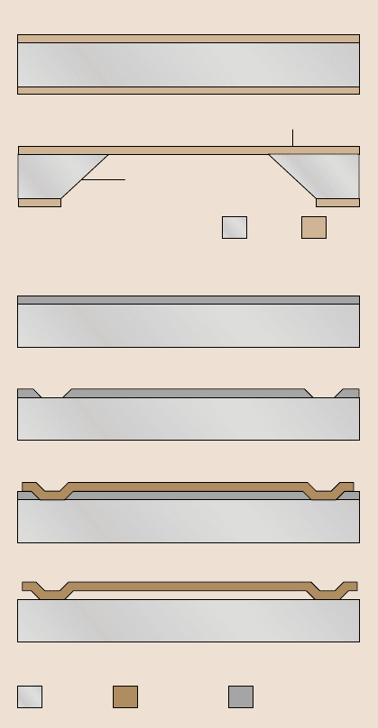
The first two approaches, bulk and surface micromachining, mostly use planar pho-
tolithographic fabrication processes developed for semiconductor devices in pro-
ducing two-dimensional (2D) structures [13, 19, 198, 199]. The various steps in-
volved in these two fabrication processes are shown schematically in Fig. 22.59.
Bulk micromachining employs anisotropic etching to remove sections through the
thickness of a single-crystal silicon wafer, typically 250–500µm thick. Bulk micro-
machining is a proven high-volume production process and is routinely used to fab-
ricate microstructures such as accelerometers,pressure sensors, and flow sensors. In
surface micromachining, structural and sacrificial films are alternatively deposited,
22 Characterization of MEMS/NEMS and BioMEMS/BioNEMS 1281
patterned, and etched to produce a freestanding structure. These films are typically
made of low-pressure chemical vapor deposition (LPCVD) polysilicon film with
a thickness of 2–20µm. Surface micromachining is used to produce sensors, actua-
tors, micromirror arrays, motors, gears, and grippers. The resolution in photolithog-
raphy is dependent upon the wavelength of light. A commonly used light source
is an argon fluoride excimer laser with a wavelength of 193nm (ultraviolet or UV)
used in patterning 90-nm lines and spaces. Deep-UV wavelengths, X-ray lithogra-
phy, electron beam (e-beam) lithography, focused ion-beam lithography, maskless
lithography, liquid-immersion lithography, and STM writing by removing material
atom by atom are some of the recent developments for sub-100-nm patterning.
The fabrication of nanostructures such as nanochannels with sub-10-nm reso-
lution can be accomplished through several routes: electron beam lithography and
sacrificial-layer lithography (SLL). The process for e-beam lithographic technique
is a finely focused electron beam that is exposed over a resist surface, where the
exposure duration and location is controlled with the use of a computer [200,201].
When the resist is exposed to the electron beam, the electrons either break or join
the molecules in the resist, so the local characteristicsare changed in such a way that
further processes can either remove the exposed part (positive resist) or remove the
unexposedpart (negative resist). The resist material determinesif the molecules will
either break or join together and thus determines if a positive or negative image is
produced. E-beam lithography can either be used to create photolithographic masks
for replication or to create the devices directly. The masks that are created can be
used for either optical or X-ray lithography. One limitation of e-beam lithography is
that throughput is drastically reduced since a single electron beam is used to create
the entire exposurepattern on the resist. While this technique is slower than conven-
tional lithographic techniques, it is ideal for prototype fabrication because no masks
are required.
In SLL process, the use of a sacrificial layer allows the direct control of
nanochannel dimensions as long as there exists a method for removing the sacri-
ficial layer with absolute selectivity to the structural layers. A materials system with
such selectivity is the silicon/silicon oxide system used widely in the microfabrica-
tion of MEMS devices. The use of sidewall deposition of the sacrificial layer and
subsequent etching allows the fabrication of high-densitynanochannels for biomed-
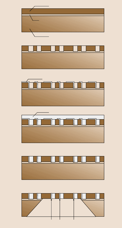
ical applications. It is based on surface micromachining [77]. Figure 22.60 shows
a schematic of the process steps in sacrificial-layer lithography based on Hansford
et al.’s [77] work on fabrication of polysilicon membranes with nanochannels. As
with all the membrane protocols, the first step in the fabrication is the etching of the
support ridge structure into the bulk silicon substrate. A low-stress silicon nitride
(LSN or simply nitride), which functions as an etch stop layer, is then deposited
using LPCVD. The base structural polysilicon layer (base layer) is deposited on top
of the etch stop layer. The plasma etching of holes in the base layer is what defines
the shape of the pores. The buried nitride acts as an etch stop for the plasma etching
of a polysilicon base layer. After the pore holes are etched through the base layer,
the pore sacrificial thermal oxide layeris grown on the base layer. The basic require-
1282 Bharat Bhushan
a)
Polysilicon
Si (100)
b)
c)
d)
e)
f)
Thermal silicon oxide
Silicon nitride
2nd Polysilicon
Silicon nanochannels
Fig. 22.60. Schematic of
process steps involved in
sacrificial-layer lithography:
(a) Growth of silicon nitride
layer (etch stop) and base po-
lysilicon deposition, (b) hole
definition in base, (c)growth
of thin sacrificial oxide and
patterning of anchor points,
(d) deposition of plug poly-
silicon, (e) planarization of
plug layer, and (f) deposition
and patterning of the pro-
tective nitride layer through
etch, followed by etching of
protective, sacrificial and etch
layers before final release of
the structure in HF [77]
ment of the sacrificial layer is the ability to control the thickness with high precision
across the entire wafer. Anchor points are defined in the sacrificial oxide layer to
mechanically connect the base layer with the plug layer (necessary to maintain the
pore spacing between layers). This is accomplished by using the same mask shifted
from the pore holes. This produces anchors in one or two corners of each pore hole,
which provide the desired connection between the structural layers while opening
as much pore area as possible. After the anchor points are etched through the sac-
rificial oxide, the plug polysilicon layer is deposited (using LPCVD) to fill in the
holes. To open the pores at the surface, the plug layer is planarized using chemical
mechanical polishing (CMP) down to the base layer, leaving the final structure with
22 Characterization of MEMS/NEMS and BioMEMS/BioNEMS 1283
the plug layer only in the pore hole openings. As the silicon wafer is ready for re-
lease, a protective nitride layer is deposited on the wafer (completely covering both
sides of the wafer). The back-side etch windows are etched in the protective layer,
exposing the silicon wafer in the desired areas, and the wafer is placed in a KOH
bath to etch. After the silicon wafer is completely removed up to the membrane
(as evidenced by the smooth buried etch-stop layer), the protective, sacrificial, and
etch-stop layers are removed by etching in concentrated HF. Etching of sacrificial
layer in polysilicon film defines nanochannels.
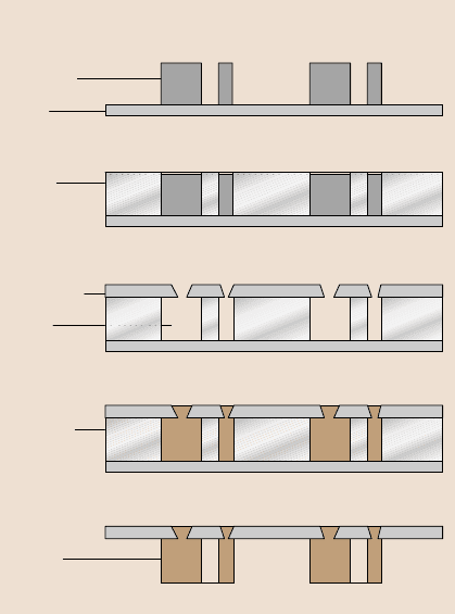
The LIGA process is based on the combined use of X-ray lithography, electro-
plating, and molding processes. The steps involved in the LIGA process are shown
schematically in Fig. 22.61. LIGA is used to produce high-aspect-ratio MEMS
(HARMEMS) devicesthat are up to 1mm in height and only a few microns in width
or length [202]. The LIGA process yields very sturdy 3D structures due to their in-
creased thickness. One of the limitations of silicon microfabrication processes orig-
inally used for fabrication of MEMS devices is the lack of suitable materials that
can be processed. With LIGA, a variety of non-silicon materials such as metals,
ceramics and polymers can be processed. Non-lithographic micromachining pro-
cesses, primarily in Europe and Japan, are also being used for the fabrication of
millimeter-scale devices using direct material microcutting or micromechanicalma-
LIGA
Resist
structure
Base
plate
Lithography
Electroforming
Metal
structure
Gate plate
Mold
insert
Mold fabrication
Molding
mass
Mold filling
Plastic
structure
Unmolding
Fig. 22.61. Schematic of the
process steps involved in
LIGA fabrication of MEMS
