Alciatore D.G., Histand M.B. Introduction to Mechatronics and Measurement Systems
Подождите немного. Документ загружается.

Confirming Pages
V
in
V
out
V
s
Figure 3.27 Optoisolator.
3.4 Bipolar Junction Transistor 101
output is protected from any excessive input voltages that could damage components
in the output circuit. Also, because the supplies and grounds are separate, any fluc-
tuations or disturbances that might occur in the output circuit have no effect on the
control signals on the input side.
(continued )
This design example illustrates an application of semiconductor optoelectronic components.
Suppose, in the design of an autonomous robot, you wish to include a laser scanning device
to sweep the environment to detect obstacles. The head of the scanner is rotated through
360 by a DC motor. Your problem here is to track the angular position of the scan head.
How could you do this if you want an on-board computer to use the sensed values?
The solution requires a sensor that provides a digital output, that is, one that can be
handled by a digital computer. We will learn more about digital interfacing in Chapter 6.
To keep the solution simple at this point, we choose a device that produces a 5 V digital
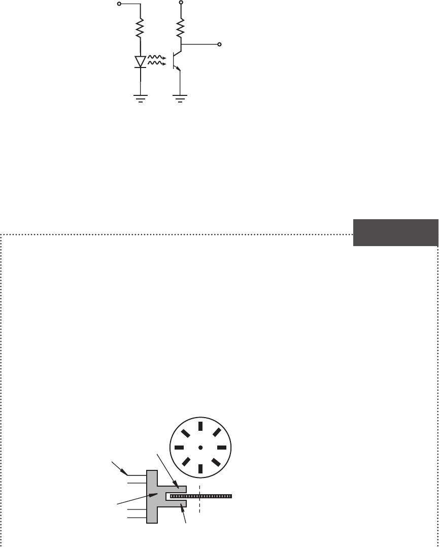
output. An LED-phototransistor pair, also known as a photo-interrupter, is at the heart of
the design, which is illustrated in the following figure. The pair, which is readily available in
a single package, produces a beam of light that can be broken or interrupted. A slotted disk
must be designed to attach to the shaft of the motor driving the scan head and to pass through
the gap in the photo-interrupter pair. Each slot in the disk provides a digital pulse as it inter-
rupts the light beam during rotation.
axis of rotation
of disk
top view o
f
slotted disk
leads
photo-interrupter
package
emitter
(LED)
side
detector
(phototransistor)
side
Angular Position of a Robotic Scanner
DESIGN
EXAMPLE 3.3
alc80237_ch03_073-116.indd 101alc80237_ch03_073-116.indd 101 1/3/11 3:47 PM1/3/11 3:47 PM
Confirming Pages
102 CHAPTER 3 Semiconductor Electronics
3.5 FIELD-EFFECT TRANSISTORS
Using what you have learned so far, you can design circuits for mechatronic systems
using BJTs and other discrete components. We now examine the field-effect tran-
sistor (FET) that operates on a different principle than the BJT but serves a similar
role in mechatronic system design. As we will see in Chapter 6, it is also an impor-
tant component in the design of digital integrated circuits.
Both the BJT and FET are three-terminal devices allowing us to draw analo-
gies between their function and how they are used in circuits. Before we look at the
details of how FETs work, we describe their general characteristics. Both BJTs and
FETs operate by controlling current between two terminals using a voltage applied
to a third terminal. In Section 3.4, we saw that the forward bias of the base-to-emitter
junction of the BJT allows charge carriers to enter a thin base region from the emit-
ter, where they are attracted to the collector, resulting in a large collector current
controlled by the much smaller base current. We concluded that the BJT is a cur-
rent amplifier. In contrast, with a FET, the electric field produced by a voltage on
one electrode controls the availability of charge carriers in a narrow region, called
a channel, through which a current can be made to flow. Therefore, a FET can be
described as a transconductance amplifier, which means the output current is con-
trolled by an input voltage.
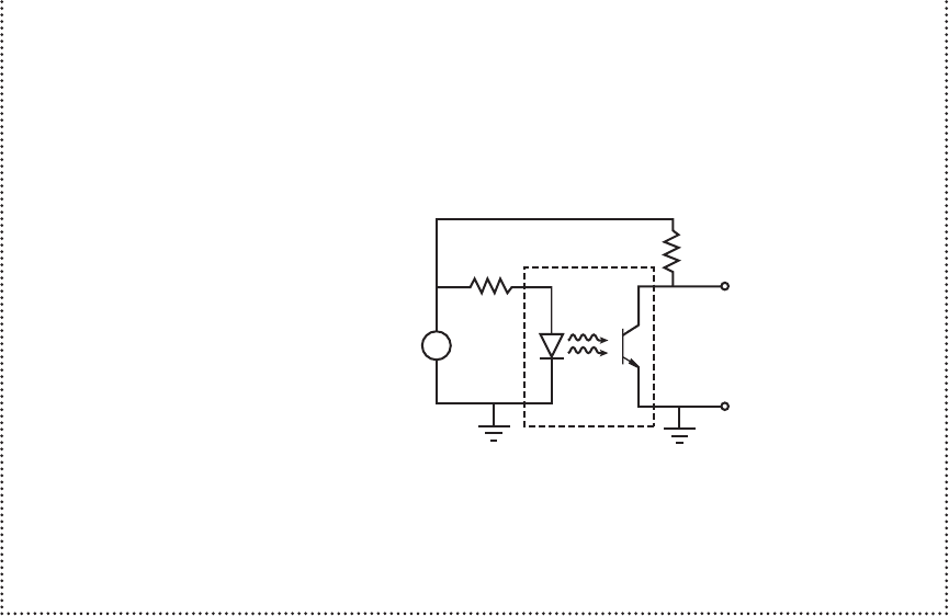
In order for the sensor to function properly, we must add the external components
shown in the following figure to provide a digital pulse each time a slot is encountered.
The emitter LED and its current limiting resistor R
1
are powered by a 5 V DC source. The
phototransistor detector and external resistor R
2
provide output signal V
out
. R
2
is called
a pull-up resistor because it pulls the output voltage ( V
out
) up from ground (0 V) to
5 V when the transistor is in cutoff. When the transistor is saturated, the output voltage
is near 0 V.
V
ou
t
+
5 V
+
–
R
1
= 200 Ω
R
2
= 1 kΩ
photo-interrupter package
As the slotted disk rotates, light passes through each slot producing a 0 V output and
then returns to 5 V when the segments between the slots interrupt the light. The result is a
train of pulses. The number of pulses produced provides the measure of angular rotation as
a digital approximation. For example, if the disk has 360 slots, each pulse would correspond
to 1 of rotation.
(concluded )
alc80237_ch03_073-116.indd 102alc80237_ch03_073-116.indd 102 1/3/11 3:47 PM1/3/11 3:47 PM
Confirming Pages
3.5 Field-Effect Transistors 103
The nomenclature describing the FET is as follows. The control electrode in
the FET, called the gate, is analogous to the base of the BJT. In contrast to the BJT
base, the FET gate draws no direct current (DC) because it is insulated from the
substrate to which it is attached. A conducting channel, whose conductivity is con-
trolled by the gate, lies between the drain, which is analogous to the BJT collector,
and the source, which is analogous to the BJT emitter. There are three families of
FETs: enhancement-mode metal-oxide-semiconductor FETs (MOSFETs), deple-
tion mode MOSFETs, and junction field-effect transistors (JFETs). Each of these
families is available in p-channel and n-channel varieties. Understanding the differ-
ent families and varieties of FETs is somewhat complicated when encountering them
for the first time, so we focus primarily on the widely used n-channel enhancement-
mode MOSFET. We will see that it is a close analogy to the npn BJT.
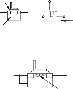
The cross section and schematic symbol for an n-channel enhancement-mode
MOSFET is illustrated in Figure 3.28 . This MOSFET has a p-type substrate and an
n-type source and drain that form pn junctions with the substrate. There is a thin sili-
con dioxide layer insulating the gate from the substrate. As illustrated in Figure 3.29 ,
when a positive DC voltage is applied to the gate, an electric field formed in the
substrate below the gate repels holes in the p-type substrate leaving a narrow layer
or channel in the substrate in which electrons predominate. This is referred to as an
n-channel in the p-type substrate. The substrate is usually connected to the source
internally so that the substrate-source pn junction is not forward biased. In the sche-
matic circuit symbol (see the right side of Figure 3.28 ), the arrowhead indicates the
direction between the p-type substrate and the n-channel.
3.5.1 Behavior of Field-Effect Transistors
Using an n-channel enhancement-mode MOSFET as our example, we explain the
details of its operation and discuss the characteristic curves analogous to the BJT.
If the gate is grounded ( V
g
0), no drain-to-source current I
d
flows for a positive
Figure 3.28 n-channel enhancement-mode MOSFET.
V
g
V
dd
V
ss
G
SD
V
gs
V
ds
I
d
+
_
+
_
nn
p
SiO
2
substrate
source drain
gate
Figure 3.29 Enhancement-mode MOSFET n-channel formation.
V = 0
ss
V > 0
dd
V > 0
g
+++++
n-channel
nn
p
alc80237_ch03_073-116.indd 103alc80237_ch03_073-116.indd 103 1/3/11 3:47 PM1/3/11 3:47 PM
Confirming Pages
104 CHAPTER 3 Semiconductor Electronics
drain voltage V
dd
because the drain pn junction is reverse biased and no conduct-
ing channel has formed. In this state, the MOSFET mimics a very large resistor
(~ 10
8
10
12
Ω), and no current flows between the drain and source. The MOSFET
is said to be in cutoff.
As V
gs
is gradually increased beyond a gate-to-source threshold voltage V
t
, the
n-channel begins to form. V
t
depends on the particular MOSFET considered but a
typical value is about 2 V. Then as V
ds
is increased from 0, conduction occurs in the
n-channel due to a flow of electrons from source to drain. The drain current I
d
, by con-
vention, is shown in the direction opposite to electron flow. As shown in Figure 3.29 ,
a subtle feature of the n-channel is that it is wider near the source than at the drain
because the electric field is larger due to the larger difference between V
g
and ground
at the source end and the smaller difference between V
g
and V
dd
at the drain end.
With a positive V
gs
larger than V
t
, as V
ds
is increased from 0, we enter the active
region, also called the ohmic region, of the MOSFET. In this region, as V
gs
is further
increased, the conduction channel grows correspondingly, and the MOSFET appears
to function like a variable resistor whose resistance is controlled by V
gs
. However,
when V
gs
V
t
reaches V
dd
, there is no longer an electric field at the drain end of
the MOSFET. Therefore, the width of the n-channel shrinks to a minimum value
close to the drain resulting in what is called pinch-off. This pinch-off limits a further
increase in drain current, and the MOSFET is said to be in saturation. In saturation,
the current is almost constant with further increases in V
ds
. The drain-to-source resis-
tance, called R
on
, is minimal (usually less than 5 Ω) as it enters the saturation region.
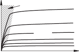
Figure 3.30 shows the characteristic family of curves for the n-channel
enhancement-mode MOSFET, which graphically illustrates the features just
described. The analogous npn BJT family of curves was shown in Figure 3.18 . By
comparing the characteristic curves, the saturation region of the MOSFET corre-
sponds to the active region of the BJT, so one must be careful when using these terms.
As we did with the npn BJT transistor, let’s look at some voltage and current
measurements from an actual MOSFET circuit, using an IRF620 power MOSFET.
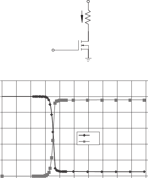
The circuit is shown in Figure 3.31a. For the experiment, the voltage on the gate
V
g
(which is also the gate-to-source voltage V
gs,
because the source is grounded)
was gradually increased from 0 to 10 V, more gradually in the ranges of interest.
Figure 3.31b shows the measurement results for the drain-to-source current I
ds
and
the drain-to-source voltage V
ds
. Notice that for this MOSFET, the threshold voltage,
Figure 3.30 n-channel enhancement-mode MOSFET characteristic curves.
I
d
V
ds
V
gs
active
region
saturation
region
alc80237_ch03_073-116.indd 104alc80237_ch03_073-116.indd 104 1/3/11 3:47 PM1/3/11 3:47 PM
Confirming Pages
3.5 Field-Effect Transistors 105
where conduction begins ( I
ds
> 0), is about 3.5 V. Also note that the drain-to-source
voltage V
ds
doesn’t drop to zero when the MOSFET is fully on. This is due to the
drain-to-source resistance R
on
of the device (see Question 3.22), which creates a
small voltage drop ( V
ds
I
ds
R
on
).
The cross section and schematic symbol for a p-channel enhancement-mode
MOSFET are illustrated in Figure 3.32 . As with the n-channel MOSFET, the arrow-
head indicates the direction of the substrate-channel pn junction. If the gate is nega-
tive with respect to the source ( V
sg
> 0), electrons in the n-type substrate are repelled,
forming a p-channel conducting layer beneath the gate. This allows a current to flow
from the source to the drain if V
sd
is positive. The p-channel enhancement-mode
MOSFET functions analogously to the pnp BJT.
MOSFETs are very useful in a variety of mechatronic applications. MOSFETs
can be used to make excellent high-current voltage-controlled switches. Also, some
MOSFETs are designed specifically as analog switches, where signals can be gated
Figure 3.31 MOSFET experiment.
V = 5 V
s
V
g
I
ds
100 Ω
+
_
V
ds
(a) test circuit
(b) results
0
01234567
Vgs (volts)
Ids (mA)
Vds (volts)
8910
1
2
3
4
5
6
0
10
20
Vds
Ids
30
40
50
60
alc80237_ch03_073-116.indd 105alc80237_ch03_073-116.indd 105 1/3/11 3:47 PM1/3/11 3:47 PM

Confirming Pages
Figure 3.33 Field-effect transistor schematic symbols.
n-channel enhancement-mode
MOSFET
p-channel enhancement-mode
MOSFET
B
S
D
G
B
S
D
G
n-channel depletion-mode JFET
S
D
G
p-channel depletion-mode JFET
S
D
G
106 CHAPTER 3 Semiconductor Electronics
(blocked or passed) in circuits. These examples are presented in Section 3.5.3. MOS-
FETs are also used in special circuits for driving DC motors. Because of their charac-
teristics, MOSFETs can be used as current sources as a result of the flat characteristics
of the saturation region. MOSFETs are also useful in the internal design of integrated
circuits (ICs) like microprocessors. The MOSFETs in ICs are often fabricated in
complementary (n-channel and p-channel) pairs, and the resulting ICs are known as
complementary metal-oxide-semiconductor (CMOS) devices. The symmetry of
the n-channel and p-channel transistors allows for compact fabrication on a single
IC and is useful in the internal design of logic devices (to be presented in Chapter 6).
3.5.2 Symbols Representing Field-Effect Transistors
Because you will come across FETs in numerous circuit designs, it is important to
recognize the subtleties of the schematic symbols for them. Because FETs (JFETs
and MOSFETs) have two different kinds of channel doping, and because the sub-
strate can be p-type or n-type, there are eight potential FET configurations. The sym-
bols for the four most important classes of FETs are shown in Figure 3.33 . The
terminal designations are G for gate, S for source, D for drain, and B for substrate.
Some of the principal characteristics of the schematic are
1 . The direction of the gate or substrate arrow distinguishes between p-channel
(arrow out) and n-channel (arrow in).
2 . A separation is shown between the gate and the source in the MOSFET but not
in the JFET. The separation represents the insulating layer of the metal oxide in
the MOSFET.
Figure 3.32 p-channel enhancement-mode MOSFET.
V
g
V
dd
V
ss
G
SD
V
sg
V
sd
I
d
_
+
_
+
pp
n
SiO
2
substrate
source drain
gate
alc80237_ch03_073-116.indd 106alc80237_ch03_073-116.indd 106 1/3/11 3:47 PM1/3/11 3:47 PM
Confirming Pages
Figure 3.34 MOSFET power switch circuit.
load
I
d
V
g
V
s
V
g
0
>V
t
V
dd
OFF
ON
flyback
diode
3.5 Field-Effect Transistors 107
3 . A broken line between the source and drain indicates an enhancement-mode
device in contrast to a solid line for a depletion-mode device. Enhancement-
mode FETs require a gate voltage for conduction, and depletion mode FETs
require a gate voltage to reduce the conduction. JFETs are available only in the
depletion mode, but MOSFETs are available in both varieties.
4 . The gate line is offset toward the source, so the source side can be easily
identified. Sometimes the gate line is shown centered; in this case there is no
way to distinguish the drain from the source unless they are labeled.
The substrate of a MOSFET may be connected to a separate terminal or inter-
nally connected to the source. If there is a separate substrate lead, it must not be
biased more positive than the source or drain for an n-channel device and must not
be biased more negative than the source or drain for a p-channel device. It should
always be connected to something (i.e., it should not be left “floating”).
3.5.3 Applications of MOSFETs
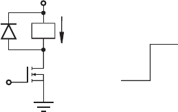
The first MOSFET application we consider is switching power to a load. This
circuit is analogous to the BJT switch presented in Section 3.4.3. An n-channel
enhancement-mode power MOSFET is used with the load on the drain side as
shown in Figure 3.34 . Note that this MOSFET switch is very easy to design
because the gate draws practically no steady state current. We must ensure that
V
g
0 for the MOSFET to be cutoff so that no current is delivered to the load.
When V
g
V
t
≈ V
dd
, the MOSFET enters saturation resulting in nearly full volt-
age V
s
across the load (because R
on
is small). The controlling parameter for the
MOSFET is gate voltage V
g
. Recall that with the BJT, the controlling parameter
is base current I
B
. With the BJT, one must ensure adequate base current to satu-
rate the BJT. Using the MOSFET, the current drawn by the gate is essentially 0,
so current sourcing is not a concern. However, one needs to calculate the drain
current I
d
and power dissipation to select a MOSFET capable of switching the
desired current for the load. Also, as with a BJT, if the load is inductive, a flyback
diode (see Figure 3.34 ) is necessary to prevent damage to the MOSFET when it
is switched off.
The second application we will consider is the use of a MOSFET as an analog
switch. Suppose you have a positive analog signal V
in
and you want to be able to
alc80237_ch03_073-116.indd 107alc80237_ch03_073-116.indd 107 1/3/11 3:47 PM1/3/11 3:47 PM

Confirming Pages
108 CHAPTER 3 Semiconductor Electronics
couple it to another circuit or device, or block it altogether. This is an easy applica-
tion for a MOSFET using the circuit shown in Figure 3.35 . If the control signal V
g
is zero, the MOSFET will be cutoff resulting in a huge drain to source impedance
(in megaohms) essentially blocking the analog signal ( V
out
0 V). The pull-down
resistor R is required to hold the V
out
terminal at ground in the off state. When the
control signal V
g
is larger than the largest value of the analog input signal V
in
plus
threshold voltage V
t
, the drain to source channel will conduct with a low resistance,
and the output signal will track the input ( V
out
V
in
).
Figure 3.35 MOSFET analog switch circuit.
V
g
V
in
V
g
0 V
> V (max)
in
V
out
R
OFF (V
out
= 0 V)
ON (V
out
= V
in
)
■ CLASS DISCUSSION ITEM 3.8
Analog Switch Limit
Considering the analog switch circuit shown in Figure 3.35 , why does the gate con-
trol signal need to be larger than the largest value of the analog signal?
Circuit to Switch Power
Among the general problems in a mechatronic system design is delivering electrical power
to different portions of the system. MOSFETs are useful devices for this task.
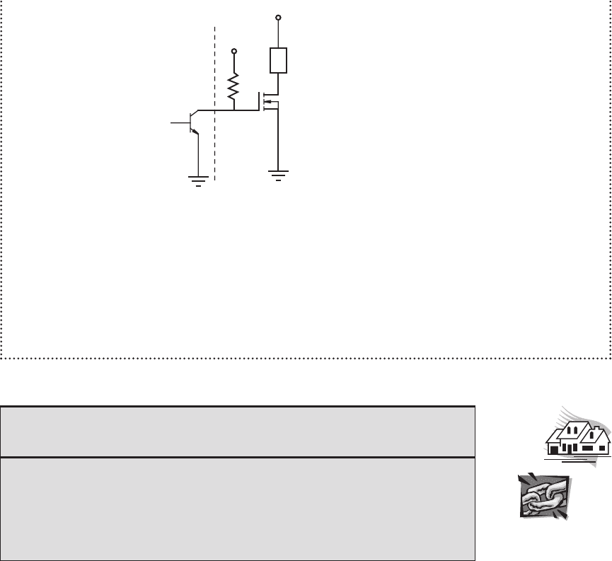
Suppose you have a digital device that produces a binary output, which means its out-
put can be one of two states. For the moment, assume that the output circuit consists of an
npn transistor that can be in cutoff or saturation, but with the collector as of yet not con-
nected to anything. As we will see later, this is called an open-collector-output device. All
you need to know for now is that the output transistor can be turned on and off. Also, it can
sink only a very small current, in the milliamp range. How then can we interface the binary
output to control the current to a load that may require a current of many amps? A solution
to this problem employing an n-channel enhancement-mode MOSFET power transistor is
shown in the following figure. The output circuit from the digital device is drawn to the left
of the dashed line, and the portion we are designing is to the right.
DESIGN
EXAMPLE 3.4
alc80237_ch03_073-116.indd 108alc80237_ch03_073-116.indd 108 1/3/11 3:47 PM1/3/11 3:47 PM
Confirming Pages
3.5 Field-Effect Transistors 109
V
s
load
power
MOSFET
open-
collector
output
5 V
R
p
digital
device
Resistor R
p
, connected to the collector lead to complete the digital output circuit, is
called a pull-up resistor because it “pulls up” the collector voltage to a DC power source
(in this case 5 V). It results in 0 V at the MOSFET gate when the output transistor is
on, and 5 V at the gate when it is off. To drive a load requiring a current larger than what
the digital output can provide, we use a power MOSFET to switch a different power
supply V
s
.
Now if you are given the specific current and voltage requirements for a load (e.g., a
motor), you can refer to manufacturer or supplier data to select the appropriate MOSFET to
do the job.
■ CLASS DISCUSSION ITEM 3.9
Common Usage of Semiconductor Components
Cite specific examples in your experience where and how each of the following
electrical components is used:
■ Signal and power diodes
■ Light-emitting diodes
■ Signal and power transistors
Internet Link 2.4 provides links to various resources and vendors for all types of
electronic components, including all of the devices presented in this book. Electron-
ics vendors provide a wealth of online information to make it easy to find data and
place orders for their products. Internet Link 3.2 provides links to the largest manu-
facturers of semiconductor components. The semiconductor manufacturers provide
a wealth of useful online information for all sorts of integrated circuits. Internet Link
3.3 is an excellent resource providing a thorough review of semiconductor physics,
devices, application circuits, and circuit analysis.
Internet Lin
k
2.4Electronic
component online
resources and
vendors
3.2Semicon-
ductor (IC)
manufacturers
and online
resources
3.3All about
circuits–Vol. III–
semiconductors
alc80237_ch03_073-116.indd 109alc80237_ch03_073-116.indd 109 1/3/11 3:47 PM1/3/11 3:47 PM
Confirming Pages
110 CHAPTER 3 Semiconductor Electronics
QUESTIONS AND EXERCISES
Section 3.3 Junction Diode
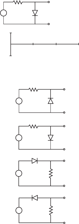
3.1. Sketch the output waveform for V
out
in the following circuit on axes as shown.
Assume the diode is ideal.
+
+
–
V
out
1 kΩ
V
in
= 10 cos(2πt)
10
–10
volts
0
V
out
1 s23
3.2. Sketch the output V
out
on a set of axes for circuits “a” through “f” with
V
in
1.0 sin(2 t ) V. Assume the diodes are ideal. Plot the output for one complete
cycle of the input (0 t 1s).
+
+
–
1 kΩ = R
V
in
V
out
(a)
+
+
–
R
V
in
V
ou
t
(b)
+
+
–
R
V
in
V
ou
t
(c)
+
+
–
R
V
in
V
out
(d)
alc80237_ch03_073-116.indd 110alc80237_ch03_073-116.indd 110 1/3/11 3:47 PM1/3/11 3:47 PM
