Alciatore D.G., Histand M.B. Introduction to Mechatronics and Measurement Systems
Подождите немного. Документ загружается.

Confirming Pages
V
B
V
E
V
C
I
C
I
B
I
E
V
BE
V
CE
> 0
V
CE
V
BE
> 0
+
–
+
–
base (B)
collector (C)
emitter (E)
n
n
p
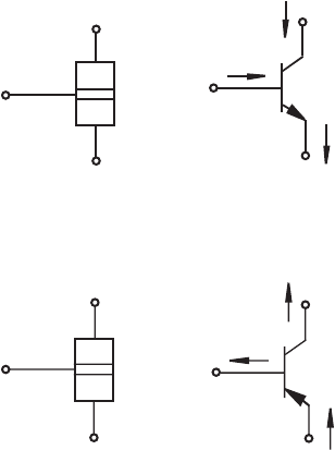
Figure 3.15 npn bipolar junction transistor.
Figure 3.16 pnp bipolar junction transistor.
V
B
V
E
V
C
I
C
I
B
I
E
–V
BE
V
CE
< 0
–V
CE
V
BE
< 0
+
–
+
–
base (B)
collector (C)
emitter (E)
p
p
n
3.4 Bipolar Junction Transistor 91
The most common type is the npn BJT, which we discuss in detail and use in our
examples. As shown in Figure 3.15 , it consists of a thin region or layer of p-type
silicon sandwiched between two regions or layers of n-type silicon. Three leads are
connected to the three regions, and they are called the collector, base, and emitter.
As denoted by the bold n in Figure 3.15 , the n-type silicon in the emitter is more
heavily doped than the collector, so the collector and emitter are not interchangeable.
The corresponding circuit schematic symbol is also shown in the figure with currents
and voltages defined and labeled. The construction, schematic, and notation for the
pnp BJT is shown in Figure 3.16 . The remainder of this section focuses on the npn
bipolar junction in Figure 3.15 .
V
CE
is the voltage between the collector and emitter, and V
BE
is the voltage
between the base and emitter. The relationships involving the transistor currents and
voltages follow:
I
E
I
C
I
B
+=
(3.10)
V
BE
V
B
V
E
–=
(3.11)
V
CE
V
C
V
E
–=
(3.12)
For the transistor to be on, the base-to-emitter junction must be forward biased
( V
BE
0.7V, so V
B
V
E
0.7V). When this is the case, a large collector current can
flow (I
C
> 0) with a small base current ( I
B
<< I
C
), and there will be a small voltage
drop ( V
CE
) in the collector-to-emitter circuit ( V
E
V
C
V
CE
).
alc80237_ch03_073-116.indd 91alc80237_ch03_073-116.indd 91 1/3/11 3:46 PM1/3/11 3:46 PM
Confirming Pages
92 CHAPTER 3 Semiconductor Electronics
T o understand how the npn BJT functions, we begin by considering the base-
to-emitter junction. Because this junction is forward biased ( V
B
> V
E
), electrons
diffuse from the emitter n-type region to the base p-type region. Because the base-
to-collector junction is reverse biased ( V
C
> V
B
), there is a depletion region that
would ordinarily prevent the flow of electrons from the base region into the col-
lector region. However, because the base region is manufactured to be very thin
and the emitter n-type region is more heavily doped than the base, most of the
electrons from the emitter accelerate through the base region with enough momen-
tum to cross the depletion region into the collector region without recombining with
holes in the base region. Remembering that conventional current is in the opposite
direction of electron motion, the result is that a small base current I
B
flows from the
base to the emitter and a larger current I
C
flows from the collector to the emitter.
The small base current controls a larger collector current, and therefore the BJT
functions as a current amplifier. This characteristic can be approximated with the
following equation:
I
C
= βI
B
(3.13)
which states that the collector current is proportional to the base current with an
amplification factor known as the beta ( ) for the transistor. Manufacturers often use
the symbol h
FE
instead of . For typical BJTs, beta is on the order of 100, but it can
vary significantly among transistors. Beta is also temperature and voltage dependent;
therefore, a precise relationship should not be assumed when designing specific tran-
sistor circuits.
Because of the BJT’s base-collector current characteristics, it can be used to
amplify current or to simply switch current on and off. This on-off switching is the
basis for most digital computers because it allows easy implementation of a two-
state binary representation. We focus on switch design and not amplifier design in
our mechatronic applications. Amplifier design requires a more in-depth study of
BJTs and is covered thoroughly in electrical engineering microelectronics textbooks.
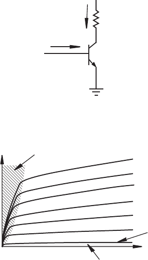
3.4.2 Common Emitter Transistor Circuit
If a BJT’s emitter is grounded and an input voltage is applied to the base, the result
is the common emitter circuit shown in Figure 3.17 . As the base current is gradu-
ally increased, the base-to-emitter diode of the transistor begins to conduct when
V
BE
is about 0.6 V. At this point I
C
begins to flow and is roughly proportional to
I
B
( I
C
I
B
). As I
B
is further increased, V
BE
slowly increases only to about 0.7 V
while I
C
rises exponentially. As I
C
rises, the voltage drop across R
C
increases and V
CE
drops toward ground. The collector cannot drop completely to ground; otherwise,
the base-to-collector pn junction would also be forward biased. When V
CE
reaches its
minimum, the transistor is said to go into saturation. In this mode, the collector cur-
rent is determined by R
C
, and the linear relation between I
C
and I
B
no longer holds.
The characteristics of the common emitter transistor circuit can be sum-
marized by plotting the collector current I
C
versus the collector-emitter voltage
V
CE
for different values of base current I
B
. The resulting family of curves (see
Figure 3.18 ) describes the common emitter characteristics for the transistor.
alc80237_ch03_073-116.indd 92alc80237_ch03_073-116.indd 92 1/3/11 3:46 PM1/3/11 3:46 PM
Confirming Pages
+
–
+
–
V
C
E
V
BE
I
B
I
C
R
C
Figure 3.17 Common emitter circuit.
Figure 3.18 Common emitter characteristics for a transistor.
I
C
V
CE
I
B
saturation
region
active
region
I
B
= 0
cutoff region
3.4 Bipolar Junction Transistor 93
The transistor has a cutoff region (where no collector current flows), an active
region (where collector current is proportional to base current), and a satura-
tion region (where collector current is strictly controlled by the collector circuit,
assuming sufficient base current). When designing a transistor switch, we need
to guarantee that the transistor is fully saturated when it is on. In full saturation,
V
CE
is at its minimum, which is about 0.2 V for a BJT. So in saturation, the base-
to-emitter junction is forward biased ( V
BE
0.7 V), there is a small drop from
the collector to the emitter ( V
CE
0.2 V), and the voltages at the leads of the
transistor are related as:
V
B
V
E
0.7 V (3.14)
V
C
V
E
0.2 V (3.15)
Example 3.4 shows how to determine how much base current and input voltage are
required to saturate a transistor. The power dissipated by the transistor ( I
C
V
CE
) is
smallest, for a given collector current, when it is fully saturated. If the transistor is
not fully saturated, it gets hot faster and can fail.
Probably the best way to understand the function of the BJT is to perform volt-
age and current measurements on actual circuits and plot the results. We’ve done
alc80237_ch03_073-116.indd 93alc80237_ch03_073-116.indd 93 1/3/11 3:46 PM1/3/11 3:46 PM
Confirming Pages
94 CHAPTER 3 Semiconductor Electronics
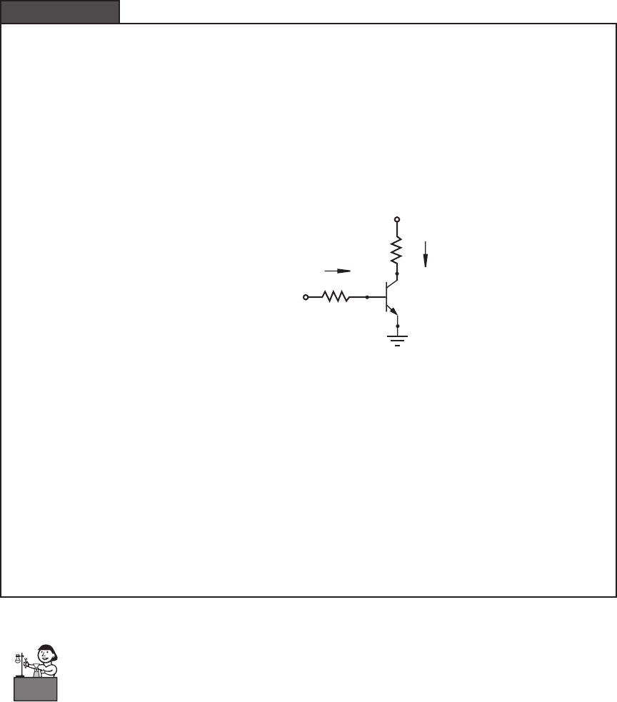
The 2N3904 is a small-signal transistor manufactured by many companies as a general pur-
pose amplifier and switch. If you examine the specifications online or in a discrete transistor
handbook, you can find a complete list of ratings and electrical characteristics. Here is some
of the information provided:
■ Maximum collector current (continuous) 200 mA
■ V
CE
(sat) 0.2 V
■ h
FE
100 (depending on collector current and many other things)
In the following circuit, what minimum input voltage V
in
is necessary to saturate the
transistor?
10 k
1 k
10 V
V
in
I
B
V
E
=
0 V
V
C
=
0.2 V
V
B
=
0.7 V
I
C
Because V
CE
(sat) for the 2N3904 is 0.2 V, when the transistor is fully saturated the collector
current is
I
C
10 V 0.2 V–
()
1k⁄Ω9.8 mA==
Because the DC current gain h
FE
is about 100, I
B
must be at least I
C
/100 or 0.098 mA.
Because V
BE
0.7 V, the base current can be related to the input voltage with
I
B
0.098 mA V
in
0.7 V–()10 k⁄Ω==
Therefore, the minimum required input voltage for saturation is
= 0.98 V + 0.7 V = 1.68 VV
in
min
Normally you would use a voltage larger than this (e.g., 2 to 5 times larger) to ensure that the
transistor is fully saturated, even with variances in parameters.
Guaranteeing That a Transistor Is in Saturation
EXAMPLE 3.4
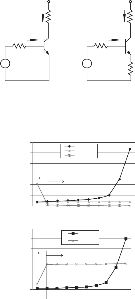
just that for the two circuits shown in Figure 3.19 , using a 2N3904 small-signal
transistor. Lab Exercise 5 also includes some experiences to help develop an under-
standing of how transistor circuits function. The first circuit ( Figure 3.19a ) is the
common emitter configuration that has been the topic of this section. The second
circuit ( Figure 3.19b ) has an additional resistor in the emitter circuit that results in
what is called emitter degeneration.
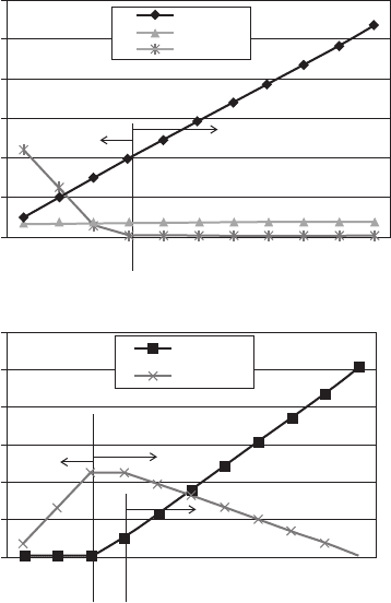
Figure 3.20 shows the results for the common emitter circuit ( Figure 3.19a ).
In Figure 3.20a , notice how the base-to-emitter forward bias voltage V
BE
and the
Lab Exercise
Lab 5Transistors
and photoelectric
circuits
alc80237_ch03_073-116.indd 94alc80237_ch03_073-116.indd 94 1/3/11 3:46 PM1/3/11 3:46 PM
Confirming Pages
+
E
B
C
+
+
V = 5 V
s
V
CE
V
BE
V
in
I
B
I
C
1k
_
_
1k
(a) common emitter
+
E
B
C
+
+
V
CE
V
BE
V
in
I
B
I
C
1k
_
_
1k
(b) emitter degeneration
1k
V = 5
V
s
Figure 3.19 Transistor experiments .
Figure 3.20 Common emitter experimental results .
0
2
4
6
8
10
12
active
region
saturation
region
Ib (mA)
Ic (mA)
(b) currents
0
2
4
6
8
10
12
Vin (V)
Vbe (V)
Vce (V)
active
region
saturation
region
(a) voltages
3.4 Bipolar Junction Transistor 95
alc80237_ch03_073-116.indd 95alc80237_ch03_073-116.indd 95 1/3/11 3:46 PM1/3/11 3:46 PM
Rev. Confirming Pages
Figure 3.21 Emitter degeneration experimental results .
0
2
4
6
8
10
12
Vin (V)
Vbe (V)
Vce (V)
active
region
saturation
region
(a) voltages
(b) currents
0
1
2
3
4
5
6
Ib (mA)
Ic (mA)
active
region
saturation
region
emitter
degeneration
96 CHAPTER 3 Semiconductor Electronics
collector-to-emitter voltage drop V
CE
do not change much after the transistor is satu-
rated, even when input voltage V
in
is increased well above the minimum required for
saturation. In Figure 3.20b , notice how the collector current I
C
does not increase in
the saturation region as the base current I
B
is increased above what is required for
saturation. As demonstrated in Example 3.4, it is important to fully saturate a transis-
tor by ensuring enough base current flows (by choosing an appropriate base resistor
for the available input voltage). However, it is also clear that increasing the input
voltage and base current significantly above the minimum required for saturation
does not provide any meaningful increase in collector current and will only result in
extra heat and energy loss in the base-to-emitter circuit.
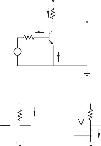
Figure 3.21 shows the results for the emitter degeneration circuit ( Figure 3.19b) .
In Figure 3.21a , notice how, just as with the common-emitter circuit, the base-to-
emitter forward-bias voltage V
BE
and the collector-to-emitter voltage drop V
CE
do
not change much after the transistor is saturated, even when input voltage V
in
is
increased well above the minimum required for saturation. In Figure 3.21b , notice
how the collector current I
C
response is very different from the response in the
common-emitter circuit. As before, saturation and maximum collector current occur
at a fairly low base current. However, as the base current is increased, the collector
alc80237_ch03_073-116.indd 96alc80237_ch03_073-116.indd 96 19/01/11 3:37 PM19/01/11 3:37 PM
Rev. Confirming Pages
+
E
B
C
+
+
+
V
C
V
ou
t
V
CE
V
BE
V
in
I
B
I
C
I
E
R
B
R
C
_
_
_
Figure 3.22 Transistor switch circuit.
Figure 3.23 Models for transistor switch states.
(b) ON
V
out
= 0
V
in
> 0.7 V
V
C
R
C
I
E
= I
B
+ I
C
(a) OFF
V
in
< 0.7 V
V
out
= V
C
V
C
R
C
I
C
= 0
0.7 V
+
–
3.4 Bipolar Junction Transistor 97
current drops. This effect is called emitter degeneration. The reason for this is that
the base current adds to the collector current, causing an increase in the emitter cur-
rent ( I
E
I
B
I
C
), creating a larger voltage drop across the emitter resistor ( I
E
R
E
).
This reduces the voltage difference across the collector resistor, resulting in less col-
lector current. The collector current actually decreases to zero as the voltage at the
emitter ( V
E
I
E
R
E
) approaches the collector supply voltage V
s
. With no voltage
difference across the collector resistor, no collector current will flow. For typical
mechatronics switching applications, the common-emitter configuration is more
appropriate because it is easy to saturate the transistor and ensure maximum collec-
tor current over a wide range of circuit parameters.
3.4.3 Bipolar Transistor Switch
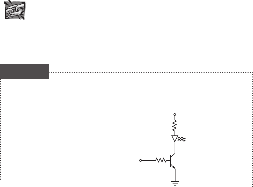
Figure 3.22 illustrates a simple transistor switch circuit. When V
in
is less than 0.7 V,
the BE junction of the transistor is not forward biased ( V
BE
< 0.7 V), and the tran-
sistor does not conduct ( I
C
I
E
0). You can therefore assume that the collector-
to-emitter circuit can be replaced by a very high impedance or, for all practical
purposes, an open circuit. This state, illustrated in Figure 3.23a , is referred to as the
cutoff or OFF state of the transistor. In cutoff, the output voltage V
out
is V
C
because
there is no current through or voltage drop across R
C
.
alc80237_ch03_073-116.indd 97alc80237_ch03_073-116.indd 97 19/01/11 3:37 PM19/01/11 3:37 PM
Confirming Pages
98 CHAPTER 3 Semiconductor Electronics
When the BE junction is forward biased ( V
BE
0.7 V), the transistor conducts.
Current passes through the CE circuit, and V
out
is close to ground potential (0.2 V
for a saturated BJT). This state, modeled by the forward-biased diode illustrated in
Figure 3.23b , is referred to as the saturated or ON state of the transistor. We assume that
there is enough base current to saturate the transistor. The resistor R
B
(see Figure 3.22 )
is required in this circuit to limit the base current because the BE junction essentially
behaves like a diode. The relationship between the base current and R
B
is given by
I
B
(V
i n
V
BE
) / R
B
(3.16)
When V
in
< 0.7, I
B
0 and V
BE
V
in
.
The circuit in Figure 3.22 can serve as a semiconductor switch to turn on or off
an LED, electric motor, solenoid, electric light, or some other load (represented by
R
C
in the figure). These loads require large currents, ranging from milliamps to many
amps, to function properly. When the input voltage and current are increased enough
to saturate the transistor, a large collector current flows through the load R
C
. The
magnitude of the collector current is determined by the load resistance R
C
and the
collector voltage V
C
. When the base-to-emitter voltage is below 0.7 V, the transistor is
off, and no current flows through the load. The transistors used in power applications,
called power transistors, are designed to conduct large currents and dissipate more
heat. Power transistors are the basis for interfacing low-output current devices such
as integrated circuits and computer ports to other devices requiring large currents.
Relays, which mechanically make and break connections, are an alternative to
transistors. They cannot switch as fast as transistors and don’t last as long, but they are
very easy to use and can switch DC as well as AC power. For more information, see
Section 10.3. AC current can also be switched with a TRIAC (triode for alternating
current), which is a semiconductor device. For more information, see Internet Link 3.1.
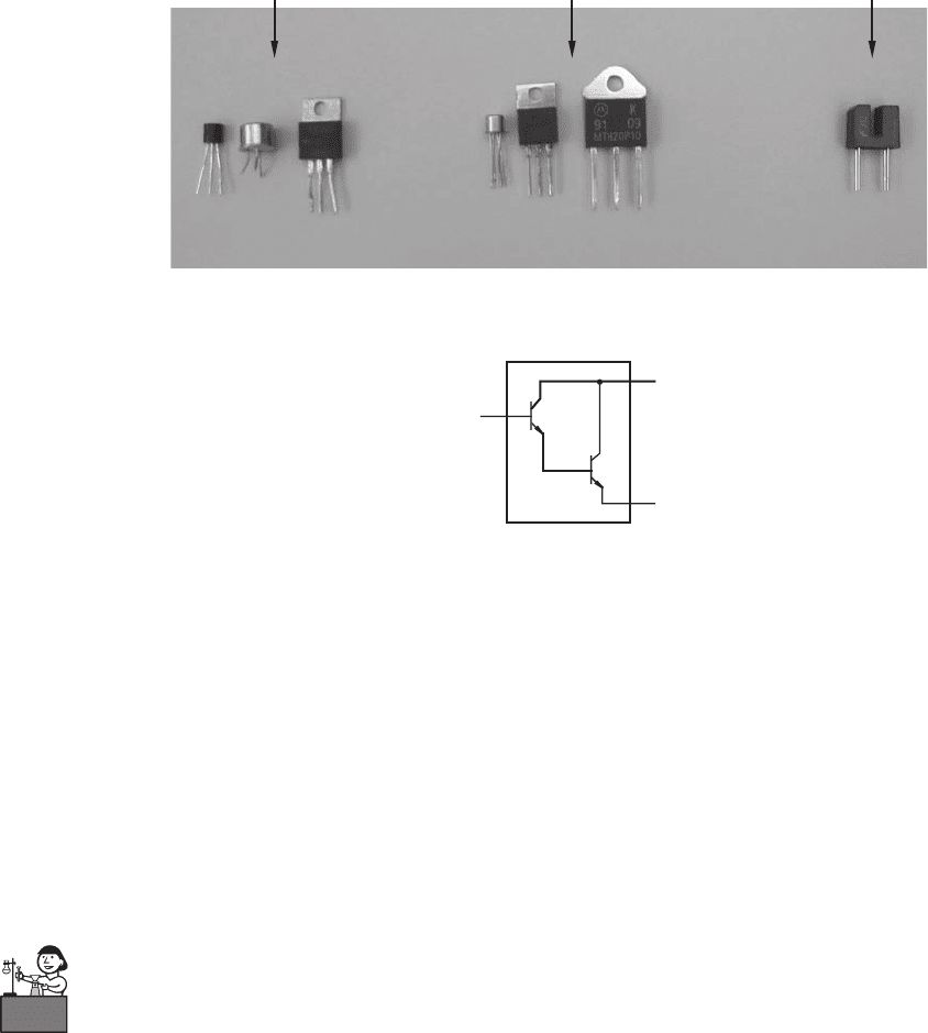
Our objective is to turn a dashboard LED on or off with a digital device having an output
voltage of either 0 V or 5 V and a maximum output current of 5 mA. The LED requires
20–40 mA to provide a bright display and has a 2 V voltage drop when forward biased.
We use a transistor switch circuit employing a small-signal transistor (e.g., 2N3904
npn) to provide sufficient current to the LED. The required circuit follows.
5 V
10 k
Ω
LED
100
Ω
digital device
output
LED Switch
DESIGN
EXAMPLE 3.2
Internet Lin
k
3.1TRIAC - triode
for alternating
current
alc80237_ch03_073-116.indd 98alc80237_ch03_073-116.indd 98 1/3/11 3:46 PM1/3/11 3:46 PM

Confirming Pages
3.4 Bipolar Junction Transistor 99
When the digital output is 0 V, the transistor is in cutoff, and the LED is OFF. When the
digital output is 5 V, the transistor is in saturation, and the base current is
5 V 0.7 V–()10
kΩ⁄ 0.43 mA=
which is within the specifications. The 100 Ω collector resistance limits the LED current to
a value within the desired range for the LED to be bright (20–40 mA):
(5 V − 2 V − 0.2 V) ⁄ 100 Ω = 28 mA
Lab Exercise 5 demonstrates how to wire and use various types of diode and
transistor circuits. Included are a basic transistor switch circuit, a motor driver circuit
with flyback protection (see Video Demo 3.2), and a photo-interrupter.
Let us summarize the guidelines for designing a transistor switch. The collec-
tor must be more positive than the base or emitter ( V
C
> V
B
> V
E
). To be ON, the
base-to-emitter voltage ( V
BE
) must be 0.7 V. The collector current I
C
is independent
of base current I
B
when the transistor is saturated, as long as there is enough base
current to ensure saturation. The minimum base current required can be estimated
by first determining the collector current I
C
and then applying I
B
min
≈ I
C
/
β.
For a
given input voltage, the input resistance must be chosen so that the base current
exceeds this value by a conservative margin (e.g., 5–10 times larger). The reasons
for this are that beta may vary among components, with temperature, and with
voltage; and the load resistance may change as current flows through it. It is also
important to calculate the maximum values of I
C
and I
B
to ensure that they fall
within the manufacturer’s specifications, and add or change series resistors if the
currents are too large.
3.4.4 Bipolar Transistor Packages
Transistor manufacturers offer their devices in a number of packages as illustrated
in Figure 3.24 . The small-signal transistor packages are often the TO-92, and the
power transistor packages are the TO-220. Surface mount technology is becom-
ing increasingly popular for use on production printed circuit boards, but such
devices are less useful for prototyping because of their small size. Figure 3.25 and
Video Demo 3.3 illustrate various common transistor packages. Included are BJTs,
metal-oxide-semiconductor field-effect transistors (MOSFETs, which are covered
in Section 3.5), and a photo-interrupter (covered in Section 3.4.6).
Lab Exercise
Lab 5Transistors
and photoelectric
circuits
Video Demo
3.2Turning a
motor on and off
with a transistor
Video Demo
3.3Transistors
CBE
BCE
C
B
E
TO-92
TO-220
SOT-23
(surface mount)
Figure 3.24 Bipolar transistor packages.
alc80237_ch03_073-116.indd 99alc80237_ch03_073-116.indd 99 1/3/11 3:46 PM1/3/11 3:46 PM
Confirming Pages
Figure 3.25 Various common transistor packages.
BJTs MOSFETs photo-interrupter
B
E
C
Figure 3.26 Darlington pair.
100 CHAPTER 3 Semiconductor Electronics
3.4.5 Darlington Transistor
The schematic in Figure 3.26 represents a transistor known as a Darlington pair,
which usually comes in a single package. The advantage of this combination is that
the current gain is the product of the two individual transistor gains and can exceed
10,000. They may often be found in power circuits for mechatronic systems.
3.4.6 Phototransistor and Optoisolator
A special class of transistor is the phototransistor, whose junction between the base
and emitter acts as a photodiode (see Section 3.3.3). LEDs and phototransistors are
often found in pairs, where the LED is used to create the light, and this light in turn
biases the phototransistor. The pair can be used to detect the presence of an object
that may partially or completely interrupt the light beam between the LED and tran-
sistor (see Lab Exercise 5).
An optoisolator is composed of an LED and a phototransistor separated by a
small gap as illustrated in Figure 3.27 . The light emitted by the LED causes current
to flow in the phototransistor circuit. This output circuit can have a different ground
reference, and the supply voltage V
s
can be chosen to establish a desired output volt-
age range. With no common ground, the optoisolator creates a state of electrical
isolation between the input and output circuits by transmitting the signal optically
rather than through an electrical connection. A benefit of this isolation is that the
Lab Exercise
Lab 5Transistors
and photoelectric
circuits
alc80237_ch03_073-116.indd 100alc80237_ch03_073-116.indd 100 1/3/11 3:46 PM1/3/11 3:46 PM
