Alciatore D.G., Histand M.B. Introduction to Mechatronics and Measurement Systems
Подождите немного. Документ загружается.

Confirming Pages
Questions and Exercises 71
+
V
s
R
1
R
2
L
C
I(t)
2.34. For each of these waveforms, what is the frequency in Hz and in rad/sec, the peak-to-
peak amplitude, and the DC offset?
a. 2.0 sin( t )
b. 10.0 cos(2 t )
c. 3.0 sin(2 t )
d. sin( ) cos( )
Section 2.7 Power in Electrical Circuits
2.35. If 100 volts rms is applied across a 100 Ω power resistor, what is the power
dissipated in watts?
2.36. If 100 volts peak-to-peak is applied across a 100 Ω power resistor, what is the power
dissipated in watts?
2.37. If standard U.S. household voltage is 120 volts rms, what is the peak voltage that
would be observed on an oscilloscope?
2.38. Write a function to represent a typical household voltage signal.
2.39. A circuit designer needs to choose an appropriate size resistor to be used in series
with a light emitting diode (LED). The LED manufacturer claims that the LED
requires 2 V to keep it on and 10 mA to generate bright light. Also, the current
should not exceed 100 mA. Assuming that a 5 V source is being used to drive the
LED circuit, what range of resistance values would be appropriate for the job? Also,
what resistor power rating would be required?
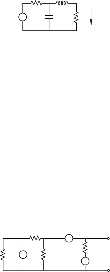
2.40. For the following circuit with R
1
1 kΩ, R
2
2 kΩ, R
3
3 kΩ, R
4
4 kΩ,
V
1
10 V, V
2
5 V, and V
3
10 V, find
a. V
out
b. the power produced by each voltage source
+
+
+
R
1
V
1
R
2
R
3
R
4
V
3
V
2
V
out
+
–
2.41. Solve the previous question with R
3
2 kΩ and R
4
1 kΩ, keeping everything else
the same.
2.42. Prove Equation 2.66 .
2.43. Derive the rms expressions in Equation 2.67 and show that Equation 2.68 is correct.
alc80237_ch02_011-072.indd 71alc80237_ch02_011-072.indd 71 1/4/11 3:43 PM1/4/11 3:43 PM
Confirming Pages
72 CHAPTER 2 Electric Circuits and Components
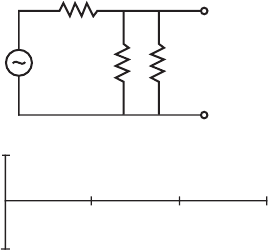
2.44. Sketch the output waveform for V
out
in the following circuit on the axes as shown:
+
+
−
V
ou
t
5 kΩ
10 kΩ
V
i
= sin(2π
t
)
10 kΩ
1
−
1
volts
0
V
out
13s2
2.45. Document a complete and thorough answer to Class Discussion Item 2.6 .
Section 2.8 Transformer
2.46. If you were to design a transformer for 24 V
rms
low-voltage lighting in a new kitchen,
what should the turns ratio of the primary to secondary windings be to provide a sat-
isfactory voltage source?
Section 2.9 Impedance Matching
2.47. If your audio stereo amplifier has an output impedance of 8 Ω, what resistance
should your speaker coils have to maximize the generated sound power?
Section 2.10 Grounding and Electrical
Interference
2.48. When making high-frequency voltage measurements with an oscilloscope, why is it
good practice to use BNC (coaxial) cable rather than two separate wires to the probe?
BIBLIOGRAPHY
Horowitz , P. and Hill , W. , The Art of Electronics, 2nd Edition, Cambridge University Press ,
New York, 1989 .
Johnson , D. , Hilburn , J. , and Johnson , J. , Basic Electric Circuit Analysis, 2nd Edition,
Prentice-Hall , Englewood Cliffs, NJ, 1984 .
Lerner , R. and Trigg , G. , Encyclopedia of Physics, VCH Publishers , New York, 1991 .
McWhorter , G. and Evans, A., Basic Electronics, Master Publishing, Richardson, TX, 1994 .
Mims , F. , Getting Started in Electronics, Radio Shack Archer Catalog No. 276-5003A, 1991 .
alc80237_ch02_011-072.indd 72alc80237_ch02_011-072.indd 72 1/4/11 3:43 PM1/4/11 3:43 PM
Confirming Pages
73
CHAPTER
3
Semiconductor
Electronics
T
his chapter presents semiconductor diodes and transistors, important for sens-
ing, interfacing, and display in mechatronic systems. ■
INPUT SIGNAL
CONDITIONING
AND INTERFACING
discrete circuits
- amplifiers
- filters
- A/D, D/D
OUTPUT SIGNAL
CONDITIONING
AND INTERFACING
- D/A, D/D
- amplifiers
- PWM
power transistors
- power op amps
GRAPHICAL
DISPLAYS
LEDs
- digital displays
- LCD
- CRT
SENSORS
- switches
- potentiometer
photoelectrics
- digital encoder
- strain gage
- thermocouple
- accelerometer
- MEMs
ACTUATORS
- solenoids, voice coils
- DC motors
- stepper motors
- servo motors
- hydraulics, pneumatics
MECHANICAL SYSTEM
- system model - dynamic response
DIGITAL CONTROL
ARCHITECTURES
- logic circuits
- microcontroller
- SBC
- PLC
- sequencing and timing
- logic and arithmetic
- control algorithms
- communication
CHAPTER OBJECTIVES
After you read, discuss, study, and apply ideas in this chapter, you will:
1. Comprehend the basic physics of semiconductor devices
2. Be aware of the different types of diodes and how they are used
3. Know the similarities and differences between bipolar junction transistors and
field-effect transistors
4. Understand how a transistor can be used to switch current to a load
alc80237_ch03_073-116.indd 73alc80237_ch03_073-116.indd 73 1/3/11 3:46 PM1/3/11 3:46 PM
Confirming Pages
74 CHAPTER 3 Semiconductor Electronics
5. Be able to design circuits using diodes, voltage regulators, bipolar transistors,
and field-effect transistors
6. Be able to select semiconductor components for your designs
3.1 INTRODUCTION
We will examine some extraordinary materials that scientists and engineers have
transformed into inventions that affect all aspects of life in the 21st century and
beyond. To understand these inventions, we need to understand the physical charac-
teristics of a class of materials known as semiconductors, which are used extensively
in electronic circuits today. We examine the physics of semiconductors, discuss how
electronic components are designed using different types of semiconductor materi-
als, learn the circuit schematic symbols for different semiconductor diodes and tran-
sistors, and use the devices in circuit design.
3.2 SEMICONDUCTOR PHYSICS AS THE
BASIS FOR UNDERSTANDING
ELECTRONIC DEVICES
Metals have a large number of weakly bound electrons in what is called their con-
duction band. When an electric field is applied to a metal, the electrons migrate
freely producing a current through the metal. Because of the ease by which large
currents can flow in metals, they are called conductors. In contrast, other materials
have atoms with valence electrons that are tightly bound, and when an electric field
is applied, the electrons do not move easily. These materials are called insulators
and do not normally sustain large electric currents. In addition, a very useful class
of materials, elements in group IV of the periodic table, have properties somewhere
between conductors and insulators. They are called semiconductors. Semiconduc-
tors such as silicon and germanium have current-carrying characteristics that depend
on temperature or the amount of light falling on them. As illustrated in Figure 3.1 ,
when a voltage is applied across a semiconductor, some of the valence electrons
easily jump to the conductance band and then move in the electric field to produce a
current, although smaller than that which would be produced in a conductor.
In a semiconductor crystal, a valence electron can jump to the conduction band,
and its absence in the valence band is called a hole. A valence electron from a nearby
atom can move to the hole, leaving another hole in its former place. This chain of
events can continue, resulting in a current that can be thought of as the movement of
holes in one direction or electrons in the other. The net effect is the same, so perhaps
Ben Franklin wasn’t completely wrong when he thought currents were the move-
ment of positive charges, the common convention used today.
The properties of pure semiconductor crystals can be significantly changed by
inserting small quantities of elements from group III or group V of the periodic table
into the crystal lattice of the semiconductor. These elements, known as dopants, can
alc80237_ch03_073-116.indd 74alc80237_ch03_073-116.indd 74 1/3/11 3:46 PM1/3/11 3:46 PM
Confirming Pages
Figure 3.1 Valence and conduction bands of materials.
conductance
band
valence
band
insulatorconductor
semiconductor
small
energy
gap
+
I
V
semiconductor with voltage applied
large
energy
gap
3.3 Junction Diode 75
be diffused or implanted into semiconductors. A thin crystal of silicon, often called a
chip, can have a minute pattern of dopants deposited on and diffused into its surface,
resulting in devices that are the basis of all modern electronics.
Properties really get interesting when different amounts and different types of
dopants are added to semiconductors. Consider what happens if dopants are embed-
ded in the crystal lattice of silicon. Silicon has four valence electrons that form sym-
metrical electron bonds in the crystal lattice. However, if arsenic or phosphorous
from group V is added to the crystal lattice, one of the five valence electrons in
each dopant atom remains freer to move around. In this case, the dopant is called a
donor element because it enhances the electron conductivity of the semiconductor.
The resulting semiconductor is called n-type silicon due to the electrons available
in the crystal lattice as charge carriers. Conversely, if the silicon is doped with boron
or gallium from group III, holes form due to missing electrons in the lattice where
the so-called acceptor dopant atoms have replaced silicon atoms. This is because
the dopant atom only has three valence electrons. A hole can jump from atom to
atom, effectively producing a positive current. What really happens is that elec-
trons move to occupy the holes, and this effectively looks like holes moving. The
resulting semiconductor is called p-type silicon due to the holes, which are effec-
tively positive charge carriers. In summary, the purpose for doping a semiconduc-
tor such as silicon is to elevate and control the number of charge carriers in the
semiconductor. In an n-type semiconductor, the charge carriers are electrons, and
in a p-type semiconductor, they are holes. As we will see shortly, the interaction
between n-type and p-type semiconductor materials is the basis for most semicon-
ductor electronic devices.
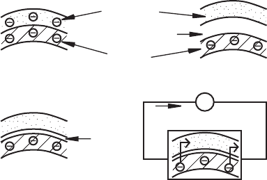
3.3 JUNCTION DIODE
Contemporary electronic devices are produced by creating microscopic interfaces
between differently doped areas within semiconductor material. If a p-type region of
silicon is created adjacent to an n-type region, a pn junction is the result. The p-type
alc80237_ch03_073-116.indd 75alc80237_ch03_073-116.indd 75 1/3/11 3:46 PM1/3/11 3:46 PM
Confirming Pages
Figure 3.2 pn junction characteristics.
p
n
cathodeanode
pn
+
V
forward biased or conduction
—
—
—
p
n
+
+
+
+
+
V
reverse biased
—
—
—
no field applied
internal contact
potential
field applied
electron
flow
pn
—
——
—
—
—
—
—
—
—
depletion
region
—
—
—
—
—
—
holes electrons
76 CHAPTER 3 Semiconductor Electronics
side of the diode is referred to as the anode, and the n-type side is called the
cathode. As illustrated in the top of Figure 3.2 , at the pn junction, electrons from
the n-type silicon can diffuse to occupy the holes in the p-type silicon, creating
what is called a depletion region. A small electric field develops across this thin
depletion region due to the diffusion of electrons. This results in a voltage differ-
ence across the depletion region called the contact potential. For silicon, the con-
tact potential is on the order of 0.6–0.7 V. The positive side of the contact potential
is in the n-type region, and the negative side is in the p-type region due to the
diffusion of the electrons. Note that we still have not connected the junction to an
external circuit.
Now, as shown in the bottom left of Figure 3.2 , if a voltage source is connected
to the pn junction with the positive side of the voltage source connected to the anode
and the negative side connected to the cathode forming a complete circuit, the diode
is said to be forward biased. The applied voltage overcomes the contact potential
and shrinks the depletion region. The anode in effect becomes a source of holes and
the cathode becomes a source of electrons so that holes and electrons are continu-
ously replenished at the junction. As the applied voltage approaches the value of the
contact potential (0.6–0.7 V for silicon), the current increases exponentially. This
effect is quantitatively described by the diode equation:
I
D
I
0
e
qV
D
kT
----------
1–
⎝⎠
⎜⎟
⎛⎞
=
(3.1)
where I
D
is the current through the junction, I
0
is the reverse saturation cur-
rent, q is the charge of one electron (1.60 10
19
C), k is Boltzmann’s constant
(1.381 10
23
J/K), V
D
is the forward bias voltage across the junction, and T is the
absolute temperature of the junction in Kelvin.
If, as shown in the bottom right of Figure 3.2 , the anode is connected to the
n-type silicon and the cathode to the p-type silicon, the depletion region is enlarged,
inhibiting diffusion of electrons and thus current; and we say the junction is reverse
biased. A reverse saturation current ( I
0
) does flow, but it is extremely small (on
the order of 10
9
to 10
15
A).
alc80237_ch03_073-116.indd 76alc80237_ch03_073-116.indd 76 1/3/11 3:46 PM1/3/11 3:46 PM
Confirming Pages
I
+–
+–
anode cathode
p
n
schematic
symbol
example
device
IN314
forward-biased
current flow
Figure 3.3 Silicon diode.
small
signal
diode
light-emitting diodes
(LEDs)
2-digit, 7-segment
LED display
power
diode
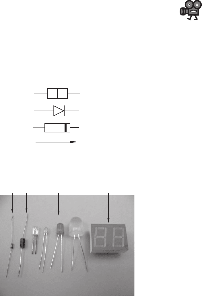
Figure 3.4 Examples of common diodes.
3.3 Junction Diode 77
Therefore, a pn junction passes current in only one direction. It is known as a
silicon diode and is sometimes referred to as a rectifier. The schematic symbol for
the silicon diode is included in Figure 3.3 . Figure 3.4 and Video Demo 3.1 show
examples of various common diodes. Included are a small signal diode, a small
power diode, and various types of light-emitting diodes. LEDs are described more in
Section 3.3.3, and seven-segment displays are presented in Section 6.12.1. The diode
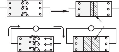
is analogous to a fluid check valve, which allows fluid to flow only in one direction
as illustrated in Figure 3.5 . We will soon see that pn junctions also occur in more
advanced devices like transistors and integrated circuits. As we will see, the on-off
action of the pn junction provides the basis for all digital devices.
Video Demo
3.1Diodes
alc80237_ch03_073-116.indd 77alc80237_ch03_073-116.indd 77 1/3/11 3:46 PM1/3/11 3:46 PM
Confirming Pages
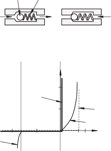
Figure 3.5 Diode check valve analogy.
open
ball spring
closed
Figure 3.6 Ideal, approximate, and real diode curves.
V
I
ideal
diode
real
diode
failure
0.7 V
*
*
failure
reverse
bias
region
forward
bias
region
breakdown
region
real
diode
approximation
of real diode
_
50 V
_
100 V 1 V
20 mA
10 mA
78 CHAPTER 3 Semiconductor Electronics
As described by Equation 3.1, the current-voltage characteristic curve for a
semiconductor diode is exponential and is shown graphically in the first quadrant of
Figure 3.6 (the curve labeled “real diode”). There is a dramatic nonlinear increase
in current as the forward bias voltage approaches 0.7 V. Note the different scales
used on the positive and negative sides of the voltage axis. In a first analysis, we
approximate the behavior of the semiconductor diode using what we call an ideal
diode model. The current-voltage characteristic curve for the ideal diode is shown
by the dark solid lines in Figure 3.6 . This model implies that the diode is fully on
for any voltage greater than or equal to 0. Also, when reverse biased, the reverse
saturation current is assumed to be 0. Later in actual circuit design, a good first
approximation for the real diode is given by the dashed lines as this replicates the
real voltage drop of 0.6 to 0.7 V measured across the silicon diode when it is for-
ward biased. In summary, an ideal diode has zero resistance when forward biased
and infinite resistance when reverse biased. For analytic purposes, it can be replaced
by a short circuit if it is forward biased and an open circuit if it is reverse biased. A
real diode requires about 0.7 V of forward bias to enable significant current flow.
When a real diode is reverse biased, it can withstand a reverse voltage up to a limit
known as the breakdown voltage, where the diode will fail as the reverse current
alc80237_ch03_073-116.indd 78alc80237_ch03_073-116.indd 78 1/3/11 3:46 PM1/3/11 3:46 PM
Confirming Pages
3.3 Junction Diode 79
increases precipitously. We will see in the next section that there is also a class of
diodes, called zener diodes, designed for use in the reverse bias region for special
applications.
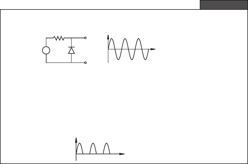
A diode is useful as a rectifier, where it passes only the positive half or the nega-
tive half of an AC signal. Example 3.1 illustrates how to analyze a simple ideal diode
circuit called a half-wave rectifier. Rectifier circuits are used in the design of power
supplies, where AC power must be transformed into DC power for use in electronic
devices and digital circuits.
The important specifications that differentiate diodes are the maximum forward
current and the maximum reverse bias voltage where breakdown occurs. The instan-
taneous surge current and average current are usually both specified, and the values
calculated for a circuit must not exceed these limits. You must also confirm that
reverse bias voltages in your circuit do not exceed the specified breakdown value.
Rectifier and power diodes are capable of carrying very large currents. They are
designed to be attached to heat sinks in order to efficiently dissipate heat produced in
the junction. Diodes require nanoseconds to switch between their on and off states.
This switching time is fast enough for most applications, but when designing high-
speed circuits it may pose a constraint.
Given the following circuit containing a diode, we will illustrate how to determine the output
voltage V
out
given a sinusoidal input V
in
.
+
+
V
in
R
V
in
V
out
t
—
A good approach to solving this problem is to analyze separately the response when
V
in
> 0 and then when V
in
< 0. When V
in
is positive, the diode is reverse biased and therefore
equivalent to an open circuit. No current flows through the resistor, and the output V
out
equals
V
in
. When V
in
is negative, the diode is forward biased, and it is equivalent to a short circuit.
Therefore, there is no voltage drop across the diode and V
out
is 0 V. Combining these two
cases, the resulting output waveform retains the positive peaks in the sine wave and loses
the negative peaks (see the following figure). Because only the positive half of the wave
remains, this circuit is known as a half-wave rectifier. Question 3.6 at the end of the chapter
deals with a full-wave rectifier.
V
out
t
Half-Wave Recti er Circuit Assuming an Ideal Diode
EXAMPLE 3.1
alc80237_ch03_073-116.indd 79alc80237_ch03_073-116.indd 79 1/3/11 3:46 PM1/3/11 3:46 PM
Confirming Pages
80 CHAPTER 3 Semiconductor Electronics
■ CLASS DISCUSSION ITEM 3.1
Real Silicon Diode in a Half-Wave Rectifier
In Example 3.1, we assumed that the diode was ideal. The first approximation to
a real diode assumes that 0.7 V is required to forward bias the diode. Using the
current-voltage relation shown by the dashed curve in Figure 3.6 , show how the
output of the half-wave rectifier would be different.
■ CLASS DISCUSSION ITEM 3.2
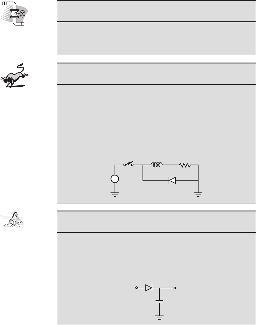
Inductive “Kick”
The following inductive circuit illustrates a common application of a diode to
reduce current arcs (sparks) between the switch contacts when the switch is opened.
Diodes used in this way are called flyback, freewheeling, or snubber diodes. Arcs
can damage the switch and can create electromagnetic interference (EMI) that can
affect surrounding circuits. Why does a switch arc when it is used to open an induc-
tive circuit? What is the purpose of the diode? Consider the current flow in the
inductor and how it changes as a function of time. Start with the switch closed and
then describe what happens when it is opened.
+
V
s
inductive load
(e.g., relay coil)
switch
■ CLASS DISCUSSION ITEM 3.3
Peak Detector
The following circuit is known as a peak detector. When a time-varying signal V
in
is applied at the input, the output V
out
retains the maximum positive value of the
input signal. Under what condition does the capacitor charge? Sketch an arbitrary
input signal and the resulting ideal output. What behavior would you expect from
an actual circuit where the capacitor is “leaky”; that is, the capacitor’s charge gradu-
ally dissipates? Draw the resulting V
out
for the “real” (nonideal) capacitor.
V
in
V
out
alc80237_ch03_073-116.indd 80alc80237_ch03_073-116.indd 80 1/3/11 3:46 PM1/3/11 3:46 PM