Zuo-Guang. Ye Advanced Dielectric Piezoelectric and Ferroelectric Materials: Synthesis, Characterisation and Applications
Подождите немного. Документ загружается.

Handbook of dielectric, piezoelectric and ferroelectric materials10
are: the maximum temperature 1365°C, temperature gradient 20 °C/cm, and
growth rate 0.4 mm/h.
The crystal-growth systems have been scaled up to grow 75mm (3 inch)
diameter crystals. Figure 1.6 shows the progress of crystal growth from 50
400 450 500 550 600
Temperature (°C)
(a)
102.0
101.5
101.0
100.5
100.0
99.5
99.0
98.5
98.0
Wt %
400 450 500 550 600 650
Temperature (°C)
(b)
100.5
100.0
99.5
99.0
98.5
98.0
97.5
Wt %
1.4
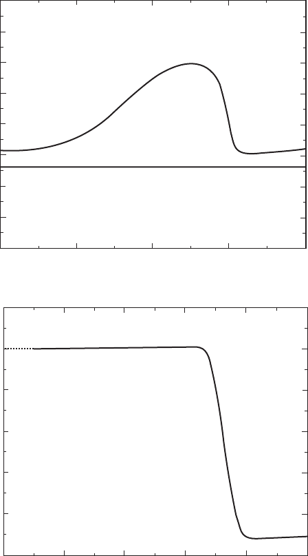
(a) PbO starts to absorb oxygen to form Pb
3
O
4
at 430° C. Pb
3
O
4
reaches maximum at 520°C. Pb
3
O
4
releases oxygen and forms PbO
as temperature continues to ramp up. (b) Pb
3
O
4
releases oxygen and
forms PbO above 600°C.
WPNL2204
Bridgman growth and properties 11
to 75 mm (2 to 3 inch) diameters. The system can deliver the following
crystal-growth conditions:
• Maximum hot-zone temperature 1600°C.
• Temperature gradient near liquid-solid interface 10–20°C/cm.
• Furnace temperature programmable with control accuracy better than
± 0.1°C at 1500°C.
• Crucible moving rate controlled by a stepping motor.
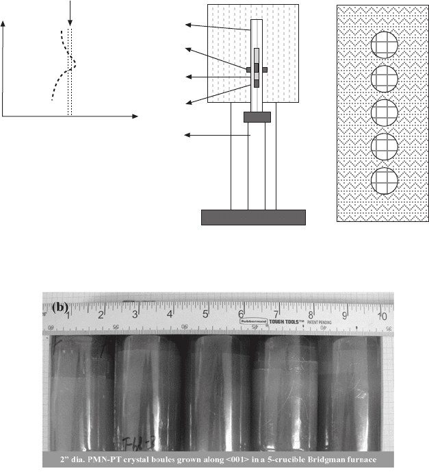
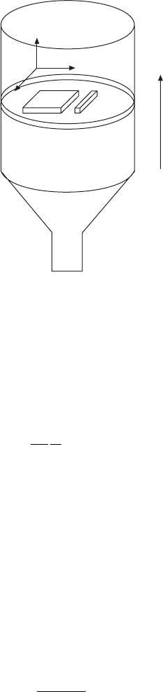
a
b
c
d
e
Temperature
Top view
Crystal-growth sytem
a. Ceramic tube liner; b. Heater; c. Crucible; d. Seed; e. Levitation mechanism.
US patent 6,972,730 B2
(a)
(b)
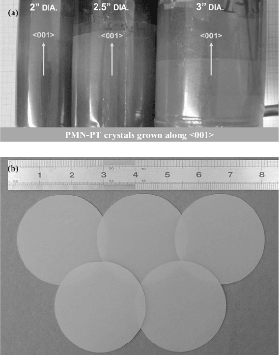
1.5
(a) Multi-crucible Bridgman growth system and (b) as-grown
PMN–PT crystal boules with 50 mm (2 inch) diameter by <001>
seeding. There are some (001) cracks perpendicular to the growth
direction in the vicinity of MPB. However, the useful segments are
crack-free.
WPNL2204
Handbook of dielectric, piezoelectric and ferroelectric materials12
• A data acquisition system monitors all parameters.
• A uninterruptible power supply (UPS) protects the control system.
• A standby natural gas electrical generator protects against power black-
out.
1.2.4 Procedures of crystal growth
The normal crystal-growth procedures are listed below:
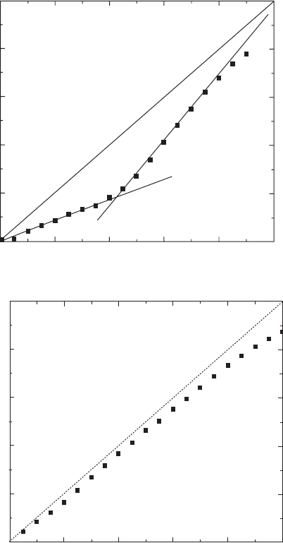
(a)
(b)
1.6
Crystal growth capacity scaled up: (a) <001>-seeded PMN–PT
crystal boules from 50 to 75 mm (2-3 inch) diameter (b); 75 mm
(3-inch) diameter (001) wafers of PMN–PT single crystal.
WPNL2204
Bridgman growth and properties 13
• Prepare the precursors free of PbO.
• Place a <001> seed of PMN–PT crystal at the bottom of the platinum
crucible, load the precursor into the crucible, and seal the top of the
crucible with a platinum lid.
• Assemble the loaded crucible into a ceramic buffer tube and fill the gap
between the crucible and the ceramic tube with alumina or zirconia
powders.
• Load the assembly into the corresponding chamber in the growth furnace
and adjust the vertical position to the initial growth site in the chamber.
• Heat up the furnace to 1350–1370°C at a rate of 100°C/h to melt the
loaded precursors.
• Soak for 2–8 h at the melting temperature, then start crystal growth by
moving down the assembly at a rate of 0.4–0.8 mm/h.
• When crystal growth is complete, ramp down the furnace temperature at
a rate of 60°C/h to room temperature.
• Unload the crucible.
1.2.5 Interface control
General speaking, one of the key parameters of the Bridgman crystal growth
is the precise control of the shape and position of liquid/solid interface. The
interface shape can be controlled to be flat or a little convex to the melt side.
However, it is difficult to keep a constant crystal-growth rate by holding the
furnace temperature unchanged. In other words, the growth rate drifts (non-
linear) to some degree due to the so-called ‘end-effect’ caused by the limited
crucible length. Experimental results indicated that the shorter the crucible
the stronger the end-effect, and that the smaller diameter of the seed, the
more severe the end-effect. Figure 1.7(a) and 1.7(b) illustrate the difference
in the end-effects for the same crucible diameter and length but different
seed diameters. It is clear that the smaller-diameter seed shows a larger drift
in growth rate. This end-effect strongly affects crystal quality and property
uniformity. In the worst case, the acceleration of the growth rate (Fig. 1.7a)
may cause constitutional supercooling that disturbs the steady growth, leading
to inclusions, micro-cracks and even unexpected nuclei.
1.3 Imperfection
In the early stage of the crystal growth, there were several typical macro-
defects such as inclusions, voids and cracks. After modification and
optimization of furnace structure and growth parameters these defects were
eliminated. In addition, the compositional homogeneity was improved by
zone leveling and by increasing growth length.
WPNL2204
Handbook of dielectric, piezoelectric and ferroelectric materials14
However, some special imperfections related to domain structures need to
be better understood. One is the oxygen deficiency in as-grown PMN–PT
crystals. The crystal becomes dark gray instead of light yellow. Although the
dark gray color can be bleached by post-annealing (e.g. 600 °C for 10 h, in
air) the domain structures remain cloudy and irregular and the physical
Crucible diameter: 41
mm
Seed diameter: 15
mm
0 20406080100
Moving length (%)
(a)
100
80
60
40
20
0
Growth length (%)
Crucible diameter: 41
mm
Seed diameter: 31
mm
0 20406080100
Moving length (%)
(b)
100
80
60
40
20
0
Growth length (%)
1.7
The influence of end-effect on growth rate for different seed
diameters. Small-diameter seed leads to a stronger non-linear
growth rate at a constant crucible moving rate.
WPNL2204
Bridgman growth and properties 15
properties vary from the normal state. It is difficult to observe the detailed
domain structure using transmission electron microscopy (TEM) because
domain changes during sample preparation. Another one is the line defect,
dislocations that were observed on (111), (211) and (001) faces by chemical
etching
25
.
.
So far, there have been few reports on the influence of dislocation
density and dislocation orientations on piezoelectric properties.
Both defects mentioned above impact piezoelectric properties that
depend on the domain structure. It is almost certain that these types of defect
play a role as domain wall pinning centers to modulate or to control the
domain structure. Thus, physical properties would vary from the normal
state.
1.4 Property characterization
For a PMN–PT crystal grown from stoichiometric melt, PT content increases
along the length of the crystal due to compositional segregation. Since properties
of PMN–PT crystals are closely related to the composition
27
, variations in
piezoelectric properties are expected along the growth direction
28
. This section
reports on the systematic characterization of property variations, and their
interrelationships for a whole PMN–31%PT crystal boule grown by a normal
Bridgman method
29
.
1.4.1 Specimen preparation
To characterize property variations along the growth direction of PMN–PT
crystals, two types of specimen were prepared (Fig. 1.8). (i) Crystal plates of
7 × 7 × 0.7 mm
3
(17 pieces) and (ii) crystal bars of 7 × 0.7 × 0.7 mm
3
(17
pieces) were sectioned from one crystal boule. All of the six faces of the plates
and bars were oriented within 0.5° of the {001} planes. To ensure relative
compositional homogeneity within a specimen, the large faces of the crystal
plates, and the length direction of the crystal bars, were chosen to be normal
to the growth direction <001>. In addition, so as to minimize compositional
differences between plates and bars, each plate had a corresponding bar
sectioned from the same location within the wafer (Fig. 1.8).
1.4.2 Poling
Crystal specimen surfaces were ultrasonically cleaned before deposition of
gold electrodes by sputtering (Hummer 8 Coater, Anatech). Plates were poled
in the thickness direction (<001>), and bars along their length (<100>). The
poling field was ~5kV/cm, and the poling current was monitored to
completeness at room temperature. All of the properties were determined at
room temperature 24h after poling.
WPNL2204
Handbook of dielectric, piezoelectric and ferroelectric materials16
1.4.3 Instruments and methods
Dielectric properties
The dielectric constant K of crystal plates was calculated from geometry and
capacitance measurements
30
(HP 4294A, Agilent Technologies) at different
frequencies, according to
K
d
A
C =
1
0
ε
1.1
where K is the free (
K
33
T
, 1kHz) or clamped (
K
33
S
, 5MHz) dielectric constant,
ε
0
is the permittivity of free space, d is the specimen thickness, A is the
electrode area and C is the capacitance.
Piezoelectric properties
The longitudinal piezoelectric charge coefficient d
33
for crystal plates was
measured on a Berlincourt-type quasi-static d
33
meter (0.25N, 110Hz; model
ZJ-3B, Institute of Acoustic, Chinese Academy of Science). Values for the
longitudinal piezoelectric voltage coefficient g
33
were calculated, according
to
31
:
g
d
K
33
33
0
33
T
=
()ε
1.2
Stable d
33
values for the bars were not obtained from the meter (to be discussed
later). Instead, the values were calculated from k
33
,
s
33
E
and
K
33
T
(see below).
Growth
direction
(001)
(010)
(100)
1.8
Orientation of crystal plates and bars.
WPNL2204

Bridgman growth and properties 17
Elastic properties
Elastic constants were calculated from resonance measurements on the bars.
The frequencies for the maximum resistance f
p
and maximum conductance
f
s
of the crystal bars were determined on the impedance analyzer. The short-
circuit compliance
s
33
E
was calculated, according to
32,33
.
s
fl k
s
k
33
E
p
22
33
2
33
D
33
2
=
1
4
1
1 –
=
1
1 – ρ
1.3
where ρ is the crystal density (8.2g/cm
3
), l is the bar length (7mm) and k
33
is the electromechanical coupling factor for the longitudinal vibration.
Electromechanical coupling
The rod extensional electromechanical coupling factor k
33
(longitudinal
excitation) was determined by one of two methods depending on specimen
geometry. For the crystal plates, the coupling factor k
33,Calc
was estimated
from the free and clamped dielectric constants
34
:
k
K
K
33,Calc
2
33
s
33
T
= 1 –
1.4
For the crystal bars, the coupling factors k
33
and k
31
(transverse excitation)
were determined from the aforementioned resonance frequencies f
p
and f
s
32,33
.
k
f
f
ff
f
33
2
s
p
ps
p
=
2
tan
2
–
ππ
1.5
d
33
and g
33
calculations
From the values of k
33
, and
s
33
E
obtained for crystal bars and
K
33
T
from
crystal plates, d
33
was calculated according to
32
:
dksK
33,Calc
33
33
E
33
T
=
1.6
The more accurate
K
33
T
values obtained from crystal plates were used in the
d
33,Calc
calculation. The width-to-thickness ratio was 10:1 for plates compared
with 1:10 for bars. Similarly, the corresponding piezoelectric voltage coefficient
g
33,Calc
was calculated from Eq. (1.2).
1.4.4 Property variations
As mentioned above, the PT content for melt-grown crystals increases along
the growth direction due to compositional segregation. Accordingly, the
WPNL2204
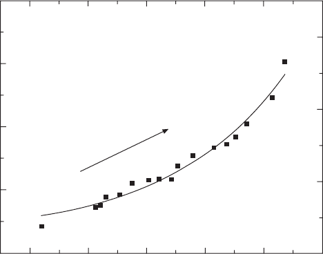
Handbook of dielectric, piezoelectric and ferroelectric materials18
ferroelectric–paraelectric transition temperature (T
C
) increases with increasing
PT content
35,36
. Thus T
C
can be used as an indicator for the composition of
PMN–PT specimens
37
. In this section, T
C
is reported as the temperature for
maximum
K
33
T
.
Dielectric constant
Figure 1.9 illustrates the dependence of
K
33
T
at room temperature on PT
content, as judged from T
C
data. Specimen 0 was close to the base of the
crystal and specimen 16 was close to the MPB. The subsequent specimens,
1 through 15, encompass the compositional range commonly used in
piezoelectric applications. For this set of specimens, T
C
increased from 121
to 142°C, which corresponded to a PT range of 26.5–32%.
K
33
T
increased
from 4400 to 7000 at room temperature with increasing PT content.
Electromechanical coupling factor and elastic compliance
k
33
and
s
33
E
values obtained for the crystal bars increased slightly with increasing
T
C
(Fig. 1.10). For example, k
33
increased from 0.84 to 0.92 (9.5%) as T
C
increased from 121°C to 142°C (i.e., 26.5% to 32% PT), with the majority
of k
33
values greater than 0.87 (Table 1.1), even though
K
33
T
and d
33
increased
significantly. In addition, k
33
appeared to approach an asymptotic value of
Plate
K
33
, 1 kHz, 0.5 V, 25 °C
T
Growth direction
R
2
= 0.976
120 125 130 135 140 145
T
C
(°C)
16
15
14
13
12
11
10
9
8
7
6
5
4
3
2
1
0
8000
7000
6000
5000
4000
K
33
T
1.9
Dielectric properties for specimens selected along the growth
direction.
WPNL2204
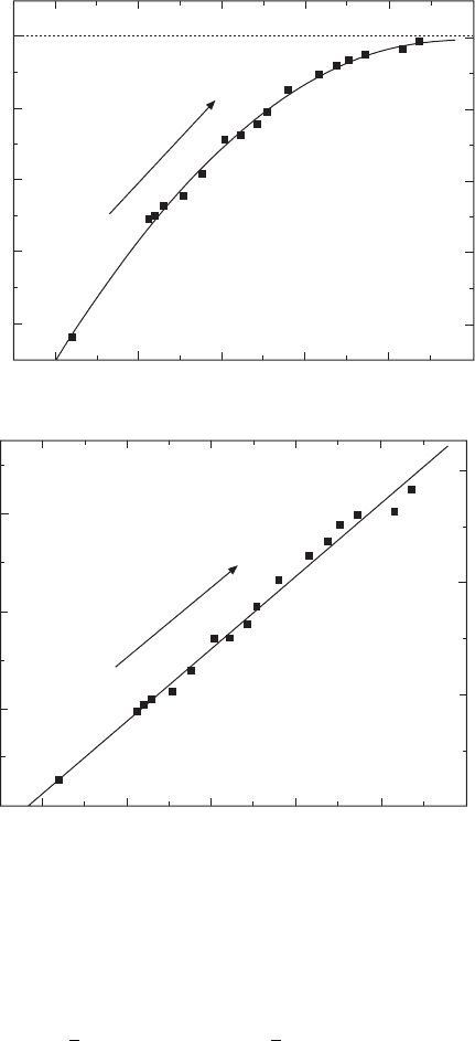
Bridgman growth and properties 19
~0.92. The calculated values of k
33
for plates from
K
33
T
and
K
33
S
data (Eq.
(1.4)) exhibited a similar trend to the k
33
values obtained from the bars by the
resonance method (Eq. (1.5)) (Table 1.1). The data obtained by calculation
and measurements (
k
33,Calc
= 0.921 and
k
33
= 0.896, respectively) are in
good agreement (<3%), giving confidence to the two independent methods
of determination for k
33
.
The
s
33
E
values obtained for crystal bars by the resonance method (Eq.
(1.3)) increased significantly from 32.6×10
–12
m
2
/N to 62.6×10
–12
m
2
/N, as
Growth direction
R
2
= 0.993
16
0
120 125 130 135 140 145
T
C
(°C)
(a)
0.92
0.90
0.88
0.86
0.84
k
33
Growth direction
16
R
2
= 0.989
60
50
40
30
120 125 130 135 140 145
T
C
(°C)
(b)
0
s
33
(× 10
–12
m
2
/N)
E
1.10
(a) Measured coupling factor and (b) calculated compliance for
bars selected along the crystal growth direction.
WPNL2204