Qin Y. Micromanufacturing Engineering and Technology
Подождите немного. Документ загружается.


MICRO-ELECTROPLATING
TECHNOLOGY
Electroplating is the key step in the fabrication of
metallic micro-components and tools such as
masks and molding tools . Established routine
processes are often referred to by simply giving
the name of the plating solution. However, every
user performs the basic process with differences in
electrolyte formulation and operation due to spe-
cific fabrication environments such as the plating
apparatus or specific material properties. Never-
theless, some general aspects in micro-electroplat-
ing will be pointed out next. From the standpoint
of a lithographic pattern, an ideal plating solution
has the following properties:
*
the resist structures are not changed (no swell-
ing, no thermal loading introduced);
*
the mechanical stress remains very low (a few
tens of MPa);
*
the grain structure does not change with height;
*
small and large areas grow at the same rate.
Some limiting aspects arise from the desire to
plate fairly thick layers in excess of 10 mm. This is
usually referred to as electroforming and many
commercial solutions can already be excluded.
The complexity of LIGA electroplating can best
be described using a sketch of the current-density
vs. voltage relationship (Fig. 13-9) [24].
At the onset of the net current density (1 and 2),
therateislimitedbythekineticsatthesurface.The
growth rate depends exponentially on the voltage,
so this is not a robust working point. Furthermore,
this corresponds to very low growth rates and unac-
ceptably long plating times. In region 4, the current
density is limited by diffusion of some species of
which the concentration at the cathode becomes
zero. To keep the diffusion zone small, both strong
convection and high ion concentrations in the elec-
trolyte are usually employed. Both aspects will raise
the diffusion-limited current density.
From the electroplating point of view, the lith-
ographic pattern is a nuisance. First, it distorts the
flow across the surface (Fig. 13-10(a)). On the one
hand, eddy currents may form and on the other
hand, convection into the structures, particularly
for high aspect ratios, may be completely inhib-
ited. In the latter case, the diffusion length corre-
sponds to the total resist height while, for good
convection, the diffusion length may be as small as
a few micrometers. This means that locally, the
current-density-potential relationship will vary
TABLE 13-3
Deep X-ray Software Packages Available: (a) http://www.ipal.sandia.gov/ip-
details.php?ip=4874; (b) http://www.kit.edu; and (c) tabata@se.ritsumei.ac.jp
Program & Platform Status Possibility
LEX-D
a
Dos Commercial Source: bending magnet
Optics: mirror, double
mirror, beam-stop
Dose: primary and
secondary
Development: 4 dimensions
DoseSim
b
Windows Freeware Source: bending magnet
Optics: mirror, double
mirror, beam-stop
Dose: primary
Development: 1 dimension
X3D
c
LINUX Freeware Source: bending magnet
Optics:
Dose: primary
Development: 4 dimensions
CHAPTER 13 Deep X-Ray Lithography 211
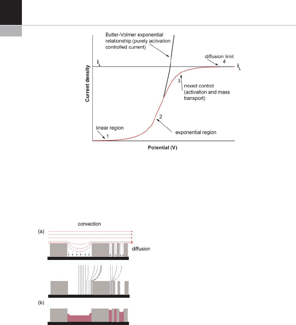
significantly. Second, the pattern distorts the
homogeneity of the electrical field, with stronger
fields corresponding to greater potentials on the
current-density-potential curve. This effect is
sketched in Fig. 13-10(b).
The ar t of elec troplating therefore involves
finding th e right chemic al composition tha t gives
the desired properties of the deposited layers and
mak ing/keeping the s olution stable against
changes associated with the electrochemical reac-
tions during plating. The lithographic pattern
introduces the requirement of low sensitivity to
local variations in potential and local var iations
in mass transport. The use of additives alters the
per formance of the plating process drastically.
Additives may be employed to change the
current-density-potential curve, where a leveler
typically makes the curve near to the operating
poi nt flatter, an inhibitor reduces the current
density at high voltages and a brightener reduce s
the potential for the same current density by
facilitating the nucleation of new grains. The
finer grains usual ly are rela ted to a great er hard-
nes s of the deposit. The electroplati ng procedures
used in the LIGA pr ocess chain are gold plating
for X-ray mask fabrication and nickel plating for
molding tools and metallic micro-components.
Further alloys may be deposited in resist molds
such as Ni-Co, Ni/P or Ni-Fe. Different plating
solution properties (bath temperature; composi-
tion; thickness accuracy; aspect ratio), which
produce a range of hardnesses of between 280
and 680 Vicker s, are listed in Table 13-4.
FIGURE 13-10 (a) Mass-transport phenomena in micro-
electroplating. The lithographic pattern may have a strong
influence on the length of the diffusion zone which, in turn,
will result in locally differing current densities, and (b) inho-
mogeneous field distribution due to the lithographic pat-
tern. Isolated small features focus the field lines and grow
faster than wider structures. The same effect leads to higher
rates near to resist edges.
FIGURE 13-9 General current-density-potential relationship [24].
212 CHAPTER 13 Deep X-Ray Lithography
The parts are typically ‘overplated’ to ensure
complete filling; an electroplating step is not able
to deliver a homogeneous thickness all over the
substrate and a polished surface, which is sometimes
needed. The top surface (electroplating front) is typ-
ically lapped and polished to the final part thickness
and aspect. Other techniques are also available:
1. Ultra-precision milling. This involves cutting
with a milling tool while the workpiece is
rotating. Using natural-diamond cutting
tools, a broad range of materials such as, for
example, non-ferrous met als (NiCo, NiP, Ni,
Au, etc.) or plastics, can be machined with a
surface roughness of below 5 nm R
a
. Only the
diamond can be sharpened to the required
level of accuracy. Cutting-edge sharpness
and roundness are crucial to the manufactured
quality of the workpiece.
2. Turning. This involves cutting with a rotating
milling tool while the workpiece is fixed.
Actually, only hard Au can be turned using
this technique;
3. Grinding and polishing. The polishing can be
effected electrolytically or chemically. All of the
techniques should meet the following criteria:
A. to deliver a good thickness-accuracy
(5 mm);
B. to avoid burr formation;
C. to deliver a specified surface quality (for
example, optical quality).
DESIGN RULE – MASK
TECHNOLOGY
A complete LIGA process database does not yet
exist. Nevertheless, the LIGA centers (CAMD,
BESSY, IMT) have accum ulated working desi gn
rules that enable them to advise customers on the
feasibility of their needs. As an example, numer-
ous parameters influence the quality of the final
parts in terms of lateral dimensions, and rough-
ness of the side wall, some of the most important
being listed here [25,26]:
*
Secondary radiation. Diverg ence of the elec-
trons and photons; fluorescence emitted by
the membrane, the absorber and the substrate;
secondary electrons emitted by the membrane,
the absorber and the substrate; and the Fresnel
diffraction; it will deposit a certain dose in the
unwanted parts of the resist.
*
Thermal distortion. The mask, resist and sub-
strate get heated during irradiation. This
leads to thermal distortion which affects the
TABLE 13-4
F&S Plating Solution Characteristics
Property Nickel Nickel/Cobalt Nickel/Iron
Composition 100 80/20 95/5
Bath temp. 40
C40
C52
C
Plating rate 12 mm/h (1 A/dm
2
)12mm/h (1 A/dm
2
)10mm/h (1 A/dm
2
)
Hardness (Vickers) 280–330 (0.1) 450–500 (0.1) 580–630 (0.1)
Thickness accuracy 50 mm 50 mm 100 mm
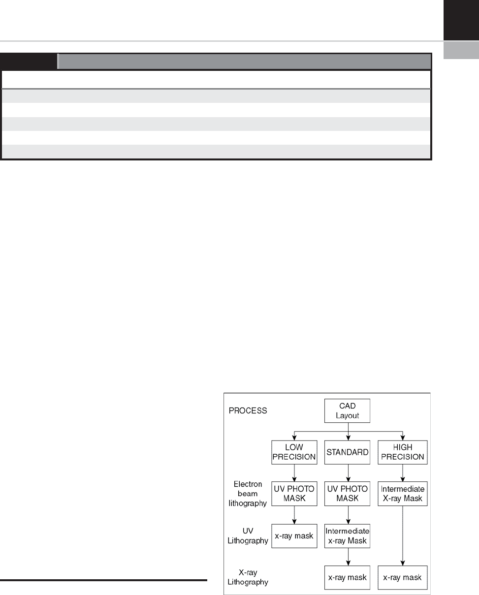
FIGURE 13-11 Different mask technology.
CHAPTER 13 Deep X-Ray Lithography 213
accuracy of the copy. Cooling of the mask and
the substrate is very important.
*
Swelling and thermal expansion of the resist.
X-ray masks are not available from commercial
mask shops as is the case for Cr masks. Therefore
the LIGA centers have developed their own tech-
nology to produce them. A variety of options exist
(see Fig. 13-11 ) requiring different tools using
different mask membranes providing different
performances for different costs (see Table 13-5).
Nevertheless, a standard exists; it is limited to the
characteristics of the support ring. X-ray masks
consist of absorber patterns (generally Au)
supported by highly X-ray transparent membranes,
the characteristics of which are given in Table 13-5.
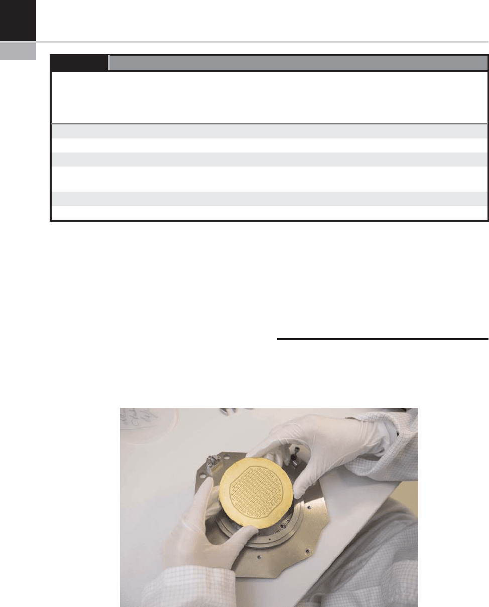
In Fig. 13-12 is shown a standard X-ray mask
(the membrane being a polished carbon mem-
brane, the layout area having a diameter of
80 mm).
METROLOGY
Micro-system technology requires 3D coordinate
measurements to be performed with measurement
precision and accuracy to within 0.1 mm. Two-
dimensional parts can be measured using
TABLE 13-5
Typical Mask-Blank Characteristics
Material Typical
Thickness
(mm)
Young’s
Modulus
(GPa)
Thermal
Expansion
Coefficient
(10
–6
/K)
Thermal
Conductivity
(W/mK)
Density
(g/cm
3
)
Price
Titanium 2 116 9 22 4.5 ++
Silicon 100 240 2.3 157 2.32 –
Beryllium 500 318 12 230 1.85 ++
Polished
carbon
150 11 8.8 96 1.8 –
Vitreous carbon 200 28 2.6 6.3 1.4 –
Diamond 30 30 1.2 1000 3.51 ++
FIGURE 13-12 A standard X-ray mask (25 m m Au absorber supported by a 160 mm polished carbon membrane).
214 CHAPTER 13 Deep X-Ray Lithography

one-dimensional measurement devic es. Three-
dimensional parts require 2D information, or a
picture, to describe them. A gear, for instance,
requires multiple measurements, including hub
diameter, pitch, addendum and dedendum circles,
involutes, top- and bottom-surface finish, side-
wall finish, side-wall angle and tooth thickness,
radius of curvature, and circularity. In addit ion,
for reliability, information about the internal
structure of the part is of great importance.
Metrology for micro-features is one of the most
active areas in dimensional metrology. Different
techniques are possible [27]; the most commonly
used being the employment of a coordinate-
measurement machine (CMM) equipped with an
optical-fiber probe [28,29].
UNIQUE FEATURES OF THE LIGA
PROCESS
Features charac terizing this process are listed
below:
1. As a result of their high energy, these
X-rays are c apable of deeply penetrating
thick (e.g. hundreds of micrometers or
even millimeters) layers of polymeric resist,
allowing the formation of tall micro-
structures in one exposure step. Very pre-
cise shape definition of parts, both laterally
in terms of dimensional control and in term
of the straightness and planarity of side
walls, are available.
2. The short wavelengths of X-ray photons pro-
vide high resolution for patterning due to low
diffraction effects. Smallest lateral dimension
of a few micrometers with structural details
in the sub-micrometer range can be manu-
factured.
3. The very small vertical angular divergence of
the X-ray beam achieves high accuracy in pat-
tern transfer from the mask. Due to their
excellent collimation, the X-rays penetrate
thick resists with extremely low horizontal
run-out (less than 0.1 mm/100 mm thickness),
thereby producing the substantially vertical
walls for which LIGA structures are well
known.
4. The almost parallel (well-collimated) light of X-
ray beams produced by synchrotron radiation
sources also allows printing with a large depth-
of-field. A large working gap between the mask
and the substrate can then be used in non-tra-
ditional pattern transfer as for the manufacture
of slanted structures or for pattern formation
on substrates presenting a large topography.
5. The vertical side walls are optically smooth
with a typical local roughness of the order of
10 nm an d longer-range waviness such as
slope errors or steps determined solely by the
accuracy of mask writing.
MARKET SITUATION OF DEEP
X-RAY LITHOGRAPHY
As mentioned earlier, the LIGA technique offers the
possibility to manufacture micro-structures with a
number of unique features. With these properties,
LIGA is on the leading edge of micro-fabrication.
This is a well-known issue to most participants in
the micro-sector. However, most of them consider
LIGA to be very expensive, to employ much time
from design-to-realization, and to invoke a number
of quality problems. They therefore try to avoid
LIGA, and only consider LIGA if the alternative
fabrication methods fail to fulfill the requirements.
These requirements, however, are often very chal-
lenging, even for LIGA, resulting in long develop-
ment times, high failure rates, and, of course, high
cost. This reinforces the above-described percep-
tion, resulting in a sort of vicious circle.
The LIGA road-map (see Fig. 13-13)defined
by IMT (Institut f
€
ur Mikrostrukturtechnik
FIGURE 13-13 Road-map to commercialization.
CHAPTER 13 Deep X-Ray Lithography 215
Karlsruhe Institute of Technology) consists of
continuous process innovation and the ability
to continually improve internal processes in the
direction of greater economy, productivity and
cost effectiveness, so that products can be offered
at lesser cost. Products that are complex and
intricately designed are often produced initially
in a prototype, low volume mode. This is espe-
cially true if the end product is very expensive. A
project named MODULIGA (modular produc-
tion method using the LIGA process) [30] linked
together the a ctivitie s of the German LIGA cen-
ters:IMT,IMM(Institutf
€
ur Mikrotechnik,
Mainz), and BESSY (Berliner Elektronenspei-
cherring-Gesellschaft f
€
ur Synchrotronstrahlung,
Berlin). The LIGA proce ss steps were standard-
ized and interface specifications were defined to
establish a modular production method. The aim
of a project named LIGA 4H (High aspect ratio,
High structure height, High dimensional accu-
racy and high sidewall quality), was to obtain a
stable manufacturing process. The next step
consists of increasing the production and of
decreasing the cost, and theoretically it should
be a s imple procedure then to move from the low
volume prototype production to high volume
production by simply adding equipment and
labour. However, the transition is much more
complex. A fully automated fabrication line
(FELIG) for dire ct LIG(A) parts in a cleanroom
environment has been built up to demonstrate
the high throughput potential of LIGA at the
ANKA synchrotron.
COMMERCIAL APPLICATIONS
Three examples are now given of commercial pro-
ducts representing the different uses of the pro-
cess. For a more complete review of applications,
see [4].
Polymer Compound Refractive X-ray
Lenses – Direct Resist Structure [5]
For hard X-rays the refractive index r in matter is
slightly less than unity. This implies a focal length
F (given as F = R/2Nr where R is the radius of the
lens) of a single concave lens (N = 1) in the range
of so me 10 meters. A compound refractive lens,
consisting of a linear arrangement of N single
lenses (see Fig. 13-14), significantly reduces the
focal length and thus can overcome this problem.
For 14 keV photons a focal spot of 0.32 mm
FIGURE 13-14 Compound refractive lens for focusing X-rays in one direction.
216 CHAPTER 13 Deep X-Ray Lithography

(FWHM) was achieved using a focal distance of
242 mm.
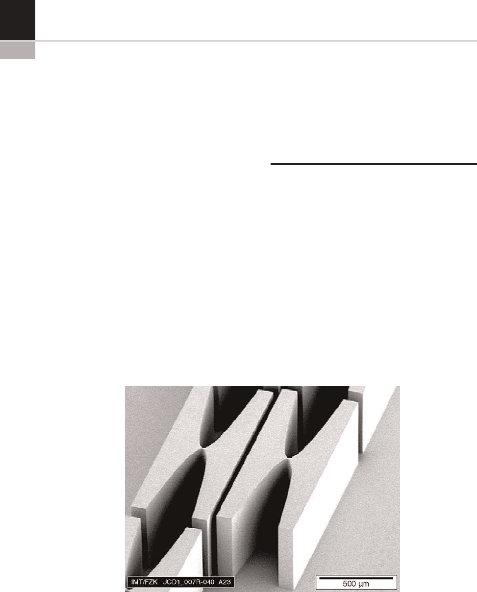
Micro-spectrometer [31] –Mold
The spectrometer, as shown in Fig. 13-15, con-
sists of a molded base-plate where the central
hollow area, the gating profile, the location of
the input fiber and the 45
mirror surface, are
produced with a single pressing. The molded
part is then placed in a vacuum chamber and
an aluminium film is deposited on both the grat-
ing surface and the mirror surface. This is then
assembled into the complete spectrograph by the
fitting of the input fiber, the central hollow
being filled with a polymer of different refractive
index t o that of the molding and a l id of the same
refractive index as that of the base that is glued
into place. The assembly is then aligned with,
and glued to, the diode array.
Micro-gears – Direct Metal Parts [32]
The search for the perfect product is one of the
major preoccupations of the luxury watch-
making industry. The combination of lithogra-
phy with electroforming offers unparalleled
machining precision and extended design f ree-
dom for the manufacture of fine parts. The SU-
8-based UV LIGA technology undoubtedly
attracts interest, in particular when competing
technologies fail to meet the precision and
quality requirements. Deep X-ray lithography
enables greater precision, better side-wall quality
and fewer restrictions, as almost any design can be
realized. As an example, the quality of the produc-
tion of gearwheels (thickness: 180 mm) in nearly
pure, but sufficiently hard, gold was addressed.
From a fabrication point of view, dimensional
quality refers to all of the parts that can be pro-
duced, the deep X-ray LIGA process showing a
process reproducibility of better than 1 mm in the
case of the example gearwheel. In Fig. 13-16, the
reproducibility of the measurement process of a
gear (in PMMA) used as a reference is presented:
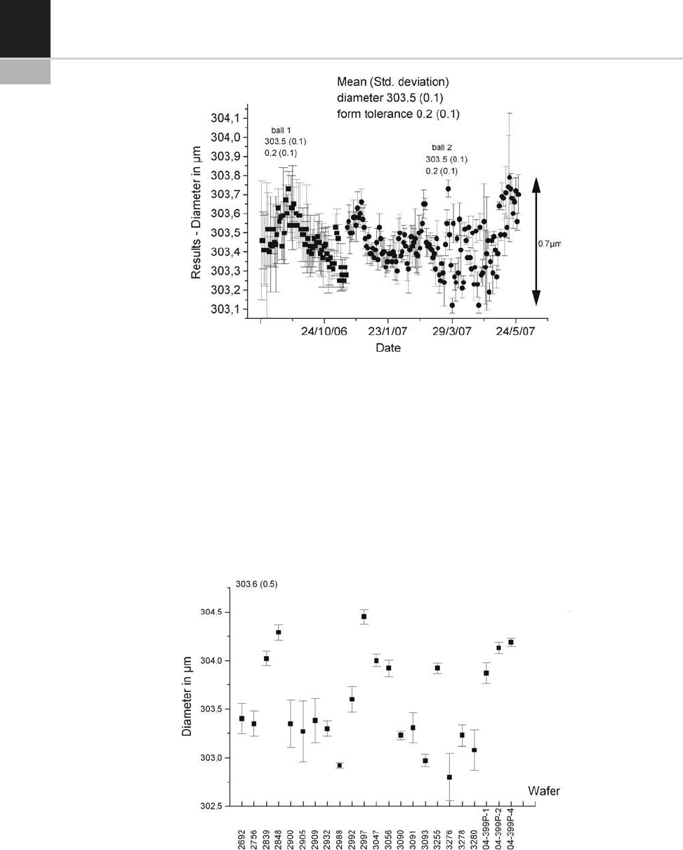
it is excellent, the standard deviation being 0.1 mm
In Fig. 13-17, the variation between about 20
wafers is presented. The diameter range min-max
is 2 mm. The FT for all the measurements is better
than 0.5 mm The process shows a reproducibility
of better than 1 mm (standard deviation:
0.5 mm). Measur ements of side-wall roughness
R
a
were performed using an atomic-force micro-
scope: all the data (R
a
) obtained are of better than
50 nm accuracy.
CONCLUSIONS
Being invented in the 1980s, the potential of LIGA
became evident in t he 1990s when numerous
examples of structures and devices were pre-
sented. The lead in MEMS technologies, how-
ever, was taken by silicon micro-machining,
and not by LIGA, despite its technical superior-
ity for many applications. The main reasons for
this are the required technical infrastructure,
FIGURE 13-15 Microspectrometer.
CHAPTER 13 Deep X-Ray Lithography 217
process knowhow, and cost issues. Silicon-
based technologies could exploit the vast tech-
nology base developed for chip-making, with
billions of dollars invested. LIGA, on the other
hand, was new a nd confined to research labo-
ratories. Furthermore , as a key process step,
LIGA required access to a synchrotron-radia-
tion facility, again a research laboratory provi-
sion, and often unacceptable for industries
establishing manufacturing plants. Neverthe-
less, and this is a demonstration of the technical
strength and superiority of LIGA, several indus-
trial LIGA products have been launched by
industries and synchrotron-radiation facilities
are currently widely used for micro-fabrication.
In addition to the described efforts to make
LIGA acceptable as a manufacturing technology
for a large variety of industrial products, cut-
ting-edge r esearch in, and with, LIGA remains a
topic of serious interest. The goals include
FIGURE 13-16 Reproducibility of the measurement process of a gear.
FIGURE 13-17 Variation between about 20 wafers.
218 CHAPTER 13 Deep X-Ray Lithography

research into new materials, new replication
techniques, and new lithographic approaches
exploiting the short-wavelength nature of
X-rays. Questions such as ‘how small can we
really get?’ and ‘can we overlap our top-down
technologies with the typical bottom-up approach
in nano-technology? At which dimensions?’ are
currently being addressed. Making devices much
smaller than is possible today will open up entirely
new fields in research and applications.
REFERENCES
[1] E.W. Becker, W. Ehrfeld, P. Hagmann, A. Maner,
D. M
€
unchmeyer, Fabrication of microstructures with
high aspect ratios and structural heights by synchro-
tron radiation lithography, galvanoforming, and
plastic moulding (LIGA process), Microelectronic
Engineering 4 (1986) 35–36.
[2] R.K. Kupka, F. Bouamrane, C. Cremers, et al., Micro-
fabrication: LIGA-X and applications, Appl. Surf. Sci.
164 (2000) 97–110.
[3] J. Hruby, LIGA technologies and applications, MRS
Bulletin 26 (4) (2001) 337–340.
[4] C.K. Malek, V. Saile, Applications of LIGA technol-
ogy to precision manufacturing of high-aspect-ratio
micro-components and -systems: a review, Micro-
electronics J. 35 (2004) 131–143.
[5] V. Nazmov, E. Reznikova, J. Mohr, A. Snigirev,
I. Snigireva, S. Achenbach, V. Saile, Fabrication and
preliminary testing of X-ray lenses in thick SU-8 resist
layers, Microsystem Technologies 10 (2004) 716–721.
[6] C. Becnel, Y. Desta, K. Kelly, Ultra-deep X-ray
lithography of densely packed SU-8 features: I. An
SU-8 casting procedure to obtain uniform solvent
content with accompanying experimental results,
J. Micromech. Microeng. 15 (2005) 1242–1248.
[7] L.J. Guerin, The SU8 Homepage, http://www.geoci-
ties.com/guerinlj/.
[8] C. Cremers, F. Bouamrane, L. Singleton, R. Schenk,
SU-8 as resist material for deep x-ray lithography,
Microsyst. Technol. 7 (2001) 6–11.
[9] M. Stewart, H. Tran, G. Schmid, T. Stachowiak,
D. Becker, G. Willson, Acid catalyst mobility in resist
resin, J. Vac. Sci. Technol. B 20 (2002) 2946–2952.
[10] H. Winick, Synchrotron Radiation Research, Chap-
ter 2: Properties of synchrotron radiation, Plenium
Press, New York (1980).
[11] G. Margaritondo, Introduction to Synchrotron Radi-
ation, Chapter 2.2: Bending magnet radiation,
Oxford University Press, New York, Oxford (1988).
[12] D. Attwood, Univ. California (Berkeley), Intro Syn-
chrotron Radiation, Bending Magnet Radiation,
EE290F (Feb. 8, 2007).
[13] A. El-Kholi, P. Bley, J. G
€
ottert, J. Mohr, Examination
of the solubility and the molecular weight distribu-
tion of PMMA in view of an optimised resist system
in deep etch x-ray lithography, Microectronic Engi-
neering 21 (1983) 271–274.
[14] M. Gad-el-Hak, The MEMS Handbook, CRC Press,
New York, USA (2001).
[15] O. Schmalz, M. Hess, R. Kosfeld, Structural changes
in poly(methyl methacrylate) during deep-etch X-ray
synchroton radiation litography. Part II: Radiation
effects on PMMA, Die Angewandte makromoleku-
lare Chemie 239 (1996) 79–91.
[16] W. Glashauser and G.V. Ghica, German patent,
3039110 (1982).
[17] J.S. Greeneich, Developer characteristics of poly-
(methyl electron resist methacrylate), J. Electrochem.
Soc. 122 (1975) 970–976.
[18] Z. Liu, F. Bouamrane, M. Rouilliay, R. Kupka,
A. Labeque, S. Metgert, Resist dissolution rate and
inclined-wall structures in deep x-ray lithography, J.
Micromech. Microeng. 8 (1998) 293–300.
[19] P. Meyer, A. El-Kholi, J. Mohr, C. Cremers,
F. Bouamrane, S. Metgert, Study of the development
behavior of irradiated foils and microstructure, SPIE
3874 (1999) 312–320.
[20] P. Meyer, A. El-Kholi, J. Schulz, Investigations of the
development rate of irradiated PMMA microstruc-
tures in deep X-ray lithography, Microelectronic
Engineering 63 (2002) 319–328.
[21] F.J. Pantenburg, S. Achenbach, J. Mohr, Influence of
developer temperature and resist material on the
structure quality in deep x-ray lithography, J. Vac.
Sci. Technol. 16 (1998) 3547–3551.
[22]P.Meyer,J.Schulz,L.Hahn,DoseSim:MS-
Windows Graphical User Interface for using synchro-
tron X-ray exposure and subsequent development in
the LIGA process, Review of Scientific Instruments
74 (2) (2002) 1113–1119.
[23] S. Hafizovic et al., X3D: 3D X-ray lithography and
development simulation for MEMS, Transducers’03
(2003) 1570–1573.
[24] M. Paunovic and M.Schlesinger, Fundamentals of
Electrochemical Deposition. The Electrochemical Soci-
ety Series, John Wiley and Sons 2nd edition (2006).
[25] S.K. Griffiths, J.M. Hruby, A. Ting, The influence of
feature sidewall tolerance on minimum absorber
thickness for LIGA x-ray masks, J. Micromech.
Microeng. 9 (1999) 353–361.
[26] S.K. Griffiths, Fundamental limitations of LIGA x-ray
lithography: sidewall offset, slope and minimum feature
size, J. Micromech. Microeng. 14 (2004) 999–1011.
[27] D. Chinn, P. Ostendorp, M. Haugh, R. Kershmann,
T. Kurgess, A. Claudet, T. Tucker, Three dimen-
sional imaging of LIGA-made microcomponents, J.
of Manufacturing Science and Engineering 126
(2004) 813–821.
CHAPTER 13 Deep X-Ray Lithography 219

[28] S. Cao, U. Brand, T. Kleine-Bestent, W. Hoffmann,
H. Schwenke, S. B€utefisch, S. B€uttgenbach, Recent
developments in dimensional metrology for micro-
system components, J. Microsystem Technologies 8
(2002) 3–6.
[29] U. Brand, J. Kirchhoff, A Micro-CMM with metrol-
ogy frame for low uncertainty measurements, mea-
surement science and technology, Meas. Sci. Tech-
nol. 16 (2005) 2489–2497.
[30] L. Hahn, P. Meyer, K. Bade, H. Hein, J. Schulz,
B. L
€
ochel, H. Scheunemann, D. Schondelmaier,
L. Singleton, MODULIGA: the LIGA process as a
modular production method-current standardization
status in Germany, Micr. Tech. 11 (2005) 240–
245.
[31] C. M
€
uller, J. Mohr, Microspectrometer fabricated by
the LIGA process, Interdisciplinary Science Reviews
18 (3) (1993) 273–279.
[32] P. Meyer, J. Schulz, L. Hahn, V. Saile, Why you will use
the deep X-ray LIG(A) technology to produce
MEMS? Microsystem Technologies 14 (9–11) (2008)
1491–1497.
220 CHAPTER 13 Deep X-Ray Lithography
