Qin Y. Micromanufacturing Engineering and Technology
Подождите немного. Документ загружается.


due to their achievable focus diameter opens up
new fields of use in micro-mechanics and micro-
electronics, such a s the replacement of thermo-
sonic ribbon bonding for high power electronics.
REFERENCES
[1] L. Bosse, N. G
€
obbels, A. Olowinsky, A. Gillner, R.
Poprawe, Production cell for laserjoining of micro-
systems with modular Pick-&-Join-tools, Proc. Third
Int. WLT-Conf. on Lasers in Manufacturing LIM
(2005) 785–789.
[2] G. Humpston, D.M. Jacobson, Principles of Solder-
ing, ASM Int, Materials Park (2004).
[3] C.F. Bohmann, The laser and microsoldering, SME
Technical + Paper No. 10: AD74-810 (1974).
[4] F. Burns, C. Zyetz, Laser microsoldering, Electronic
Packaging & Production(1981).
[5] D. Chang, Experimental investigation of laser beam
soldering, Welding J. 65 (10) (1986) 33–41.
[6] F.G. Meyer, Laserl
€
oten unter besonderer Ber
€
ucksich-
tigung der SM-Technologie und des L
€
otens an schwer
zug
€
anglichen Stellen, DVS-Verlag D
€
usseldorf (1989)
122 70–71.
[7] R. Vanzetti, A.S. Dustoomian, Intelligence comes to
laser soldering, Electronics(July 1986) 75–77.
[8] F.G. Meyer, B.H. Klimt, Laser soldering of surface
mounted devices, Proc. SPIE 744 (1987) 8–90.
[9] R. Keeler, Lasers for high-reliability soldering – for
soldering military, computer, and other high-rel pro-
ducts lasers surpass mass-soldering methods, Elec-
tronic Packaging & Production 27 (10) (1987).
[10] M. Haag, M. Brandner, Diodenlaser – innovatives
Werkzeug f
€
ur die Produktion, Proc. LaserOpto 3
(2000) .
[11] L. Bosse, A. Koglin, A. Olowinsky, V. Kolauch, M.
Nover, Laser beam soldering – an attractive alterna-
tive to conventional soldering technologies, Proc.
SPIE 4977 (2003) 473–480.
[12] L. Bosse, A. Gillner, R. Poprawe, Temperature con-
trolled selective soldering with laser radiation, Proc.
of the 6th International Symp. on Laser Precision
Microfabrication (2005).
[13] L. Bosse, A. Schildecker, A. Gillner, R. Poprawe,
High quality laser beam soldering, Microsystem
Technologies 7 (2002) 215–219.
[14] L. Bosse, A. Gillner, R. Poprawe, Adapted time-
power profile for laser beam soldering with solder
paste, Proc. SPIE 4406 (2001) 76–81.
CHAPTER 12 Laser Beam Micro-Joining 201

13
Deep X-Ray Lithography
Pascal Meyer, Joachim Schulz and Volker Saile
INTRODUCTION
By far the leading technology for the manufactur-
ing of MEMS devices is silicon micro-machining
with its various derivatives. However, many
applications of micro-systems have requirements
in respect of materials, geometry, aspect ratio,
dimensions, shape, accuracy of micro-structures,
and number of parts that cannot be fulfilled easily
by mainstream silicon-based micro-machining
technologies. LIGA, a German acronym for Lithog-
raphy (Lithographie), Electroplating (Galvanofor-
mung ), and Mol ding (Abformung) enables the
highly precise manufacture of high aspect ratio
micro-structures with large structural thickness
ranging from hundreds to thousands of micr ons.
Thes e tall micro-structu res can be produced in a
variety of materials with well-defined geometry
and dimensions, very straight and smooth side
walls, and tight tolerances. LIGA technology is
also well suited for the mass fabric ation of parts,
particularly in polymers. Many micro-syst ems
benefit from the unique char acteristics and
advantages of the LIGA process in terms of prod-
uct performance. In this chapter the strengths of
the manufacturing method and its mai n fields of
application are emphasized, with examples taken
from various groups worldwide, especially in
micro-mechanics and micro-optics.
Several micro-fabrication technologies are
available at the present time and are used to fab-
ricate micro-components and -systems. The most
successful micro-machining technologies have
been developed as extensions of standard IC and
micro-electronics planar silicon-based processing.
Others are based on advanced precision engineer-
ing and laser structuring. However, individual
technologies including Si micro-machining or laser
structuring are far from being sufficient to fulfill
the needs of the variety of problems posed by:
*
the great variety of functions of most of the
devices to be made;
*
the conditions of the surroundings in which
they will operate;
*
the optimum cost/performance ratio for the
targeted application.
Interest in a number of non-Si-based machin-
ing methods stems from major deficiencies of IC-
based machining techniques:
*
the need for using application-specific materi-
als to optimize the functions and performance
of various devices;
*
the need to reduce cost by choosing low cost
materials;
*
the difficulty in constructing truly 3D objects
with planar-based processing, which con tinues
to be a challenge.
Precision and ultra-precisi on mechanical,
electro-discharge, LIGA-based, and laser-based,
micro-machining techniques, to mention the most
current, are such alternative techniques, each with
its specific application domains and relative mer-
its. LIGA-based processing, a sequence of micro-
fabrication steps combining a step of deep X-ray
lithography (DXRL), also called by some authors
‘deep etch X-ray lithography’, and subsequent
additive processing of plating-through-mask and
molding, has moved from the position of emerging
from micro-fabrication technology to become
CHAPTER
202

a well-established non-silicon alternative micro-
fabrication technology for MEMS.
LIGA technology provides unique advantages
over other manufacturing methods in the fabrica-
tion of micro-structures. LIGA-based technolo-
gies are used and are being further developed in
a number of R&D institutes around the world.
Spin-off companies and commercial companies
have also evolved around large-scale synchrotron
facilities. Also, commercial applications of the
LIGA process are on the market. LIGA technol-
ogy has been developed over the rather long time
span of two decades [1–4]. During this time other
high aspect ratio technologies such as UV photo-
lithography in thick resist, for example as SU-8,
often referred to as UV -LIGA, and Deep Reactive
Ion Etching (DRIE) of silicon have also evolv ed
and challenged LIGA successfully in some specific
application areas. For planning the role of LIGA
in future manufacturing, a review of potential
applications may serve as a useful basis. The basic
LIGA process and some aspects of the process are
recalled here to illustrate its strengths and discuss
still existing challenges.
THE LIGA PROCESS AND ITS
STRENGTHS
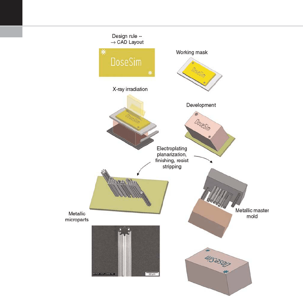
The basic LIGA process is described in Fig. 13-1 .
In the first step of the process, an X-ray-sensitive
polymer (resist) layer of up to several mi llimeters
thickness is coated onto a conductive or non-
conductive substrate. Typically polymethylmetha-
crylate (PMMA) is used as positive resist and an
epoxy-based resist SU-8 [5–9] as negative resist. A
pattern from a mask is then transferred into the
thick resist layer via a 1:1 shadow-proximity print-
ing scheme using hard X-rays from a synchrotron
radiation source. After exposure, selective disso-
lution of the chemically modified irradiated parts
of the positive resist (or dissolution of the non-
irradiated parts of the negative resist) in a chemical
developer results in a polymeric relief replica of the
mask pattern.
Then, depending on the material, number of
parts selected for the final product, accuracy,
quality and price, different fabrication routes
can be chosen, which may include further steps
of mi cro-replication through electroforming and/
or a variety of molding techniques (injection
molding, embossing, casting, compression mold-
ing, etc.). The polymeric micro-structure can be
used:
*
simply as it is;
*
as a lost mold for the formation of ceramic
micro-parts;
*
as an electroplating template to generate metal-
lic micro-parts;
*
as an ele ctroplating template to prod uce a
metallic master-mold, which can then be used
many times to mold cost-effective replicas in
other materials, primarily polymers. When
producing large numbers of electroplated com-
ponents, the molded polymer parts are used as
lost molds for a second plating pro cess.
The unique processing feature that enables the
manufacture of thick micro-structures character-
ized by very steep walls and very tight tolerances is
the creation of a high precision resist template by
deep X-ray lithography using X-ray photons from
a synchrotron radiation source.
LIGA MANUFACTURING STEPS
Resist Technology
The resist technology consists of applyin g a resist
onto a substrate, the substrates that can be used
depend on the product to be made (for example, a
mold insert), but they should meet the following
criteria:
*
a high planarity;
*
the substrate and resist should have good adhe-
sion;
*
the substrate surface should be conductive if an
electroplating step is needed;
*
the resist developer should not etch the sub-
strate.
Concerning the resist, a distinction should be
made between positive and negative resist. In the
first case, the radiation will da mage the polymer
by reducing its molecular weight; the most com-
monly used being polymethylmetacrylate
(PMMA); the irradiates parts becom ing soluble
CHAPTER 13 Deep X-Ray Lithography 203
in a developer. In the case of a negative resist, the
radiation will ‘damage’ the polymer by increasing
its molecular weight (curing/cross-linking); the
irradiated volume being insoluble in a developer;
the most commonly used of which is an epoxy-
based resin: the SU-8. In the first case, it is neces-
sary to know the dose to apply to the resist so that
it becomes soluble in the developer; while the
developer must have a negligible influence on
the non-irradiated parts; in the second case, it is
necessary to know the dose to apply to the resist so
that the exposed part becomes insoluble in the
developer. PMMA is still the resist of choice for
many applications; this resist offering very high
resolution and stable processing parameters. Its
sensitivity is low, which means high exposure
costs. SU-8 is a very attractive resist; its sensitivity
is high, reducing exposure times by a factor of 100
FIGURE 13-1 Illustration of basic LIGA process steps.
204 CHAPTER 13 Deep X-Ray Lithography

compared to PMMA. However, SU-8 actually
offers an unreliable performance due to the high
sensitivity of processing parameters’ fluctuation.
Resist Deposition
Concerning PMMA, two possibilities exist:
1. Gluing a commercially available PMMA sheet
with a glue consisting of PMMA dissolved in
methylmetacrylate (MMA). Prior to gluing,
the PMMA sheet is cut and milled to the
desired dimensions, the stress so induced
being removed by annealing under controlled
ramping conditions (the max temperature is
slightly above the glass transition tempera-
ture of the PMMA used). The positioning of
the sheet and the dispersing of the glue can
be made using a robotic dispenser combined
with a pick-and-place machine. This method
is generally used for PMMA thicknesses greater
than 100 mm.
2. Casting. A resin consisting of PMMA dis-
solved in MMA is mixed with di-benzoylper-
oxide and dimethylaniline, and is applied to
the substrate and hardened under a pressure
of 4 bar at room temperature for 4 h; the
dispensing can be effected using a robot dis-
penser. Subsequently, the resist-coated sub-
strate is annealed under ramping conditions.
This method is generally used for PMMA
thicknesses of less than 100 mm.
The SU-8 is spin coated. Expe rimental results
indicate that the coating qualities of SU8 are
affected by several factors, including the spinning
speed, the photoresist viscosity, the initial accel-
eration and the duration. After the resist has been
applied to the substrate, it must be soft baked to
evaporate the so lvent and densify the film.
Irradiation Technology
LIGA technology needs a synchrotron beam-
line to perform the resist exposure, a scanner
to move the sample through the line shaped
beam, and a c omputer program to c alculate the
dose.
Synchrotron Source – Scanner. At the heart
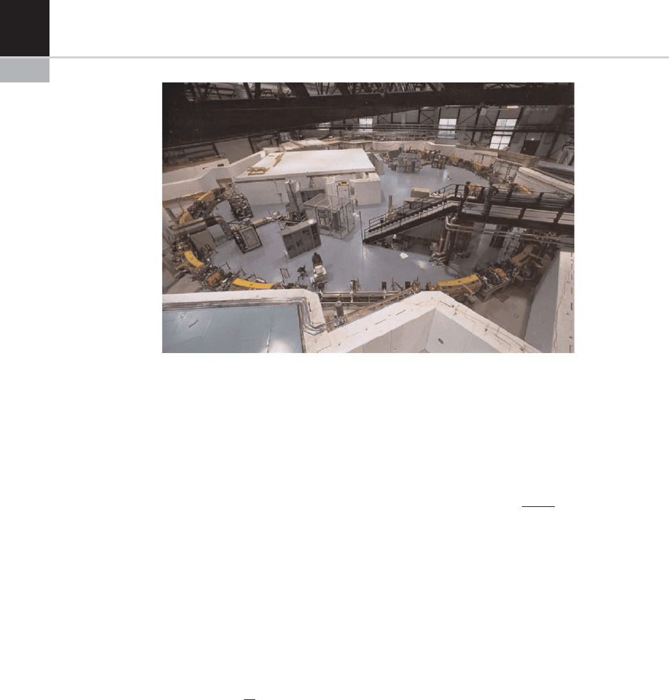
of a synchrotron (see Figs. 13-2 and 13-3) is a
storage ring: a huge donut -shaped vacuum cham-
ber. Electrons are accelerated and confined to
travel around the storage ring at nearly the
speed of light [10–12]. Because the electrons are
constantly forced to travel in a closed loop they
are accelerated, and accelerated electrons lose
energy in the form of synchrotron light. A
synchrotron produces light of exceptional quality
and brightness: a million times more intense
than that of a hospital X-ray machine. A
FIGURE 13-2 Schematic view of a synchrotron (source: Soleil).
CHAPTER 13 Deep X-Ray Lithography 205
charged particle that is constrained to move in a
curved path experie nces centripetal accelera-
tion. Due to this acceleration, the particle radi-
ates energy according to the Maxwell equations.
A non-relativistic partic le emits radiation pri-
marily at its frequency of revolution. However,
as the speed of the particle approaches the speed
of light, the radiation pattern is distorted by
relativistic effects a nd changes to a narrow cone
of radiation with angular spread. The total
energy E for a particle of mass at rest m
0
moving
at velocity n is:
E ¼ gm
0
c
2
ð1Þ
with
g ¼ 1
ffiffiffiffiffiffiffiffiffiffiffiffiffiffiffiffiffiffiffiffi
1
v
2
c
2
s
ð2Þ
The opening angle Dw of the radiation cone can
be expressed, for high values of g, as:
Dw ffi g
1
ð3Þ
Synchrotron radiation sources produce
photons with a continuum of energies, from the
infrared to the X-ray region. The spectral range of
photons produced by electrons (energy E
e
(GeV))
in a bending magnet (radius of curvature: R
b
,
magnet field: B (T)) can be characterized with
the critical energy E
c
, where:
E
c
¼
3h
--
cg
3
2R
b
ð4Þ
In practical units, the critical photon energy is
also given by:
E
c
ðKeVÞ¼0:6650E
2
e
ðGeVÞBðTÞð5Þ
E
c
is defined in terms of the spectral power radi-
ated by a relativistic particle: half of the power
spectra is radiated at energies below E
c
and the
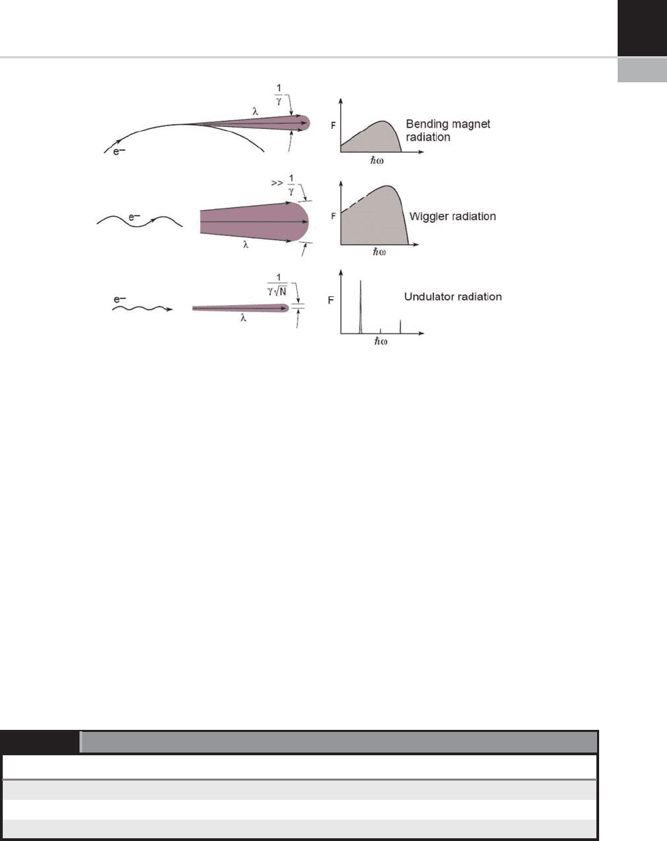
other half at energies above it. A wiggler (a series
of magne ts designed to periodically horizontally
deflect the charged particle) and an undulator (a
series of magnets designed to periodically verti-
cally deflect the charged particle) are also used to
produce synchrotron radiation, the differences of
which are indicate d in Fig. 13-4.
Presented in Ta ble 13-1 is a non-exhaustive
list of synchrotrons with install LIGA beam-
lines.
For example, the synchrotron ANKA in Karls-
ruhe (Germany) is a third-gene ration, medium-
FIGURE 13-3 View of the synchrotron ANKA.
206 CHAPTER 13 Deep X-Ray Lithography
energy source, with an electron beam energy of
2.5 giga electron volts. The X-rays are sent into
the various beam-lines (the straight lines branch-
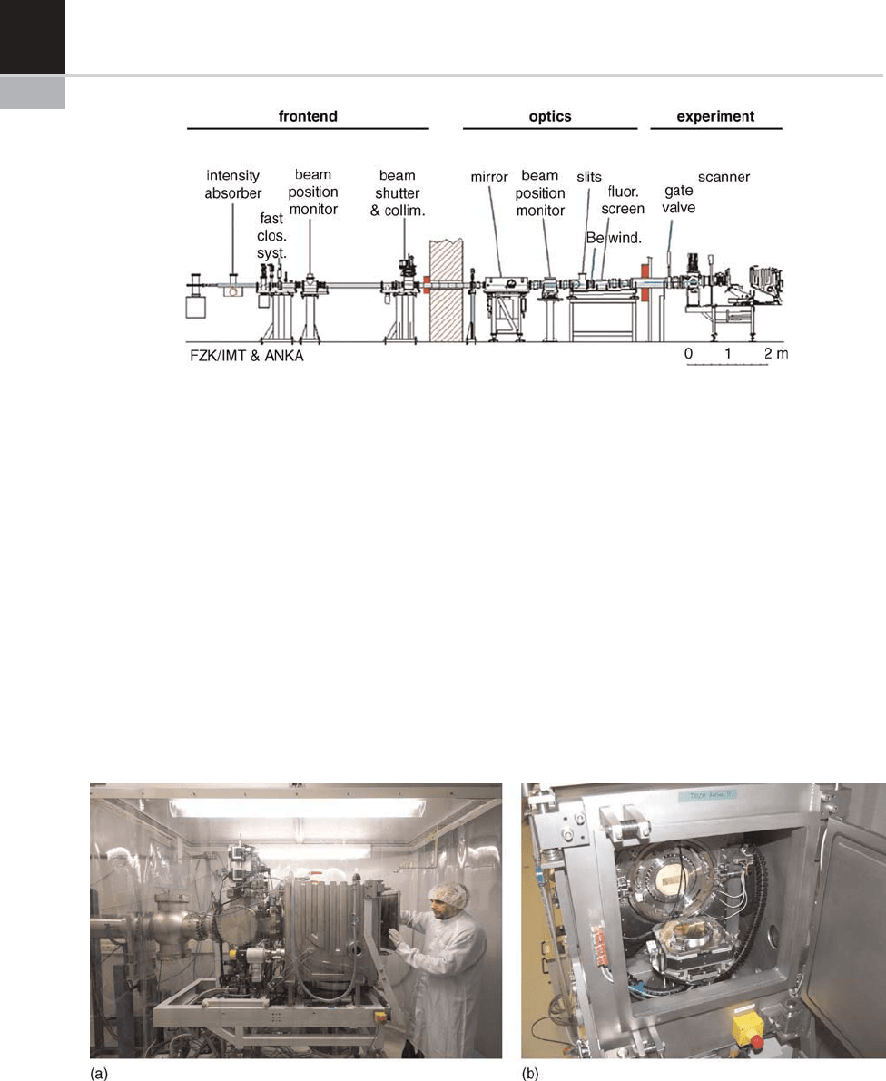
ing out of the synchrotron). A typical LIGA beam-
line is presented in Fig. 13-5. All of the beam-lines
are equipped with a scanner (see Fig. 13-6), and
optical elements which modify the spectrum of
the source. In fact, the synchrotron spectrum
should be adapted to the needs of the user. The
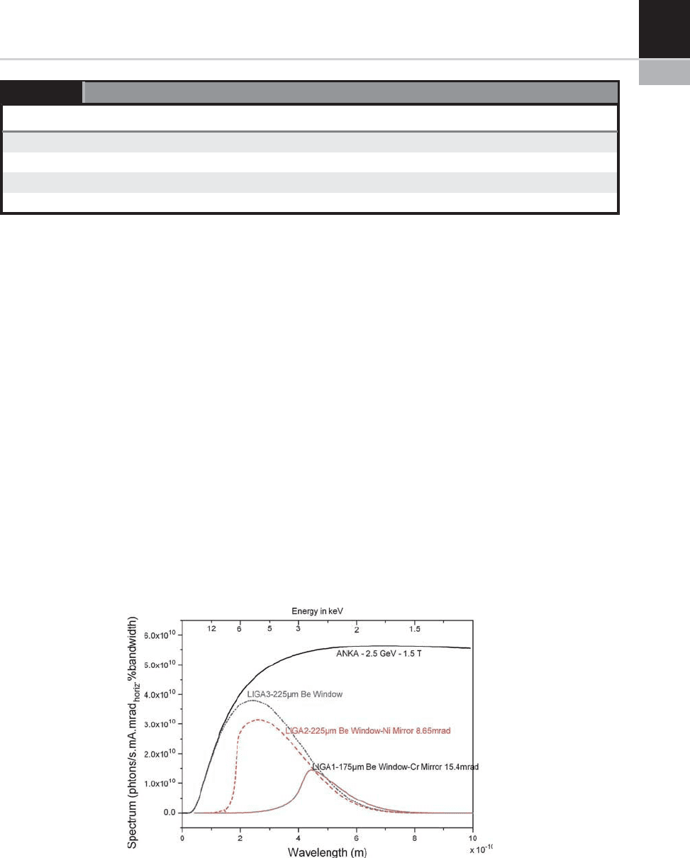
synchrotron ANKA has three LIGA beam-lines
(LIGA1, LIGA2, LIGA3) sited on a bending mag-
net (1.5 T) with different optics. The characteris-
tics of the beam-lines are given in Table 13-2. The
spectra of the lines after the front end wind ow and
optics are given in Fig. 13-7. The X-rays produced
are highly parallel and to conserve this property
for the lithography aspect, the diffraction (Fres-
nel) effect should be as low as possible and also the
absorption of the photons should take place only
in the designed volume. In X-ray lithography,
typically X-rays in the 0.5–5 10
10
m region are
used, which interact with matter by the photoelec-
tric effect, the Com pton effect, and Rayleigh
scattering. The total effect depends on the cross-
section of the different possibilities of interaction.
The primary dose, which is about 95% of the
deposited dose, is due to the photoelectric effect
in PMMA. Incident photon energy will be dissi-
pated ultimately by secondary electrons generated
by impact ionization; the distance over which the
energy is spread should be as small as possible.
The resolution limit of X-ray lithography is a
TABLE 13-1
Synchrotron Location and Operating Energy (this is a Non-Exhaustive List)
Name BESSY ANKA ELETTRA CAMD AURORA
Country/City Germany/Berlin Germany/Karlsruhe Italy/Trieste USA/Baton Rouge Japan/Kyoto
Operating energy (GeV) 1.7 2.5 1.7 1.3 0.575
Nb. of LIGA beam-lines 2 3 1 4 4
FIGURE 13-4 Different sources of synchrotron radiation with some of their characteristics.
CHAPTER 13 Deep X-Ray Lithography 207
function of diffraction in the mask-to-sample gap,
and the effective range of the photo and auger
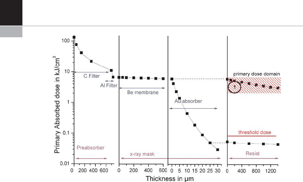
electrons related when an X-ray is absorbed. In
Fig. 13-8, it is shown how the spectrum (source
synchrotron ANKA; beam-line LIGA3) is attenu-
ated during the exposure of a 1400 mm PMMA
sample. The carbon and aluminum filters absorb
the low energy radiation to prevent overexposure
of the top surface; the primary dose to be depos-
ited in the resist should be situated in the region
D
bottom
to D
top
. This region has been determined
by many tests and is the best compromise between
exposure and development time. The mask mem-
brane (beryllium) is quasi-transparent, as it is
required. The absorber thickness should be a
minimum, defined by the threshold dose at which
the resist starts to dissolve.
PMMA Degradation. During X-ray irradiation
of PMMA, synchrotron light is absorbed in the
exposed PMMA area, which results in a chemical
modification; a scission of the polymer chain leads
to a radiation-induced degradat ion of the molec-
ular weight and becomes soluble in an organic
developer. By increasing the dose of radiation,
the average molecular weight decreases from an
initial value M
WDose¼0ðÞ
(about 1.5 10
6
g/mol) to a
minimum limiting value of between 2500 g/mol
and 3000 g/mol at a very high dose of radiation.
The degradation mechanism of radiation-excited
PMMA depends on the chemical structure of the
FIGURE 13-6 (a) Side and front (scanner open) view of the Jenoptik scanner – beam-line: ANKA-LIGA3, and (b) side
and front (scanner open) view of the Jenoptik scanner – beam-line: ANKA-LIGA3.
FIGURE 13-5 Schematic diagram of an X-ray lithography beam-line (ANKA-LIGA2).
208 CHAPTER 13 Deep X-Ray Lithography
resist and the exposure energy. The radiochemis-
try of PMMA is a complex mixture of consecutive
reactions including excitations, fissions, cross-
linking, recombinations, disproportions, rearran-
gements and transfer reactions. The most impor-
tant step of degradation is the scission of the
methyl ester group, which is responsible for the
major amoun t of the gases evolved. The rem ain-
ing polymer chain stabilizes after hydrogen
abstraction by formation of a double bond or by
chain scission. Radio-chemical degradation of
PMMA is categorized into two schemes:
1. About 80% of the main-chain scissions have
been observed after preceding side-chain deg-
radation. The radiation-excited polymer mol-
ecule splits off an ester side-chain. The
remaining chain radical stabilizes after hydro-
gen abstraction by the formation of a double
bond, or reacts by way of a main-chain scis-
sion. In the case of stabilization by hydrogen
abstraction, the molecule has one ester side-
chain less than before irradiation.
2. The remaining 20% of the main-chain scis-
sions are due to the direct decomposition of
the polymer into two macro-molecules.
Recombination of these fragments results in
the primary polymer molecule.
PMMA Development. The dissolution rate is a
function of molecular weight, which is related to
the initial PMMA molecular weight, the dose
and the main-chain scission yield [13–21]. This
reduction of the average molecular weight
causes the solubility of the resi st in the developer
to increase dramatically. A developer suitable
for PMMA in X-ray lithography, commonly
referred to as the GG developer, is composed
of 15 vol% deionized water, 60 vol% 2-(2-
butoxyethoxy)ethanol, 20 vol% tetrahydro-1-4-
oxazine and 5 vol% 2-aminoethanol. For X-ray
lithography process simulation to calculate
TABLE 13-2
Some Characteristics of the Three LIGA Beam-lines of the Synchrotron ANKA
Beam-line LIGA1 LIGA2 LIGA3
Window 175 mm beryllium 225 mm beryllium 350 mm beryllium
Optics single Cr mirror single Ni mirror no optics
Dedicated to X-ray lithography deep X-ray lithography Ultra-deep X-ray lithography
Structure height up to 100 mm 100 to 600 mm 600 to 2500 mm
FIGURE 13-7 Spectrum of the three LIGA beam-lines at ANKA, Germany.
CHAPTER 13 Deep X-Ray Lithography 209
high aspect ratio micro-structures and realistic
MEMS devices of the size order of mm, a mac-
roscopic resist dissolution and an easily m easur-
able approach are required, rather than to
describe the very complicated problem of micro-
scopic resist dissolution. In chemistry, many
models concerning polymer dissolution may be
found. Due to the fact that a dose profile is
deposited during X-ray lithography and the GG
developer consists of four components, these
models cannot be applied easily. The dissolution
rate is described by t he following equation (all
other parameters being constant):
RD
ðÞ
¼ R
0
þ C M
W Dose¼DðÞ
b
ð6Þ
R
0
corresponds to the development r ate of an
unexposed resist M
WDose¼0ðÞ
(R
0
is negligible
in the case of the PMMA-GG system), and C
and b are characteristic constants of the polymer
and solvent.
In reality, the relationship between the dissolu-
tion rate a nd the dose is influenced by a large
number of parameters related to chemical reac-
tion at the liquid (GG developer) – solid (PMMA)
interface, e.g. the PMMA molecule weight, the
developer temperature and the development
apparatus.
Special Computer Programs for X-ray
Lithography. Different computer programs have
been developed, which meet the requirements of a
LIGA X-ray beam-line [22,23]. The code cur-
rently pe rmits the computation of synchrotron
radiation from bending magnets, the effects of
the optical properties of materi als, and the nec-
essary parameters for the resist expos ure. The
basic calculations ne eded for synchrotron beam-
line design ar e related to the spectral character-
istics and to the mod eling of the optical elements
(mirrors,filters,beam-stop).Forexample,the
following calculations are performed: the dose
rate, th e dose profile from the top to the bottom
of the re sist, the exposure do se (the parameter
which should be given to the scanner which
moves the sample) and the time needed to develop
an irradiated resis- sample. In Table 13-3 are
listed computer programs especia lly dedicated
to deep X-ray l ithography.
FIGURE 13-8 Primary absorbed dose along the X-ray trajectory, including a 1400 mm thick PMMA foil X-ray mask with a
550 mm beryllium membrane and carbon and aluminum filters. The source is ANKA; the beam-line is LIGA3.
210 CHAPTER 13 Deep X-Ray Lithography
