Qin Y. Micromanufacturing Engineering and Technology
Подождите немного. Документ загружается.

Basic Tools for Hot Embossing
The requirements and concepts underlying the
design of tools for hot embossing were described
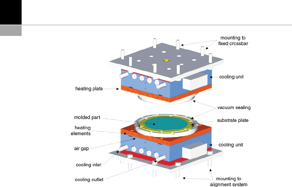
above. An example of a hot embossing tool with
an optimized heating and cooling concept was
developed at the Institute of Microstructure Tech-
nology at the research center of Karlsruhe. In this
case, thermal mass is reduced, while the stability
and evenness of the surfaces needed for molding
micro-structures on large areas of a thin residual
layer are maintained (Fig. 5-14).
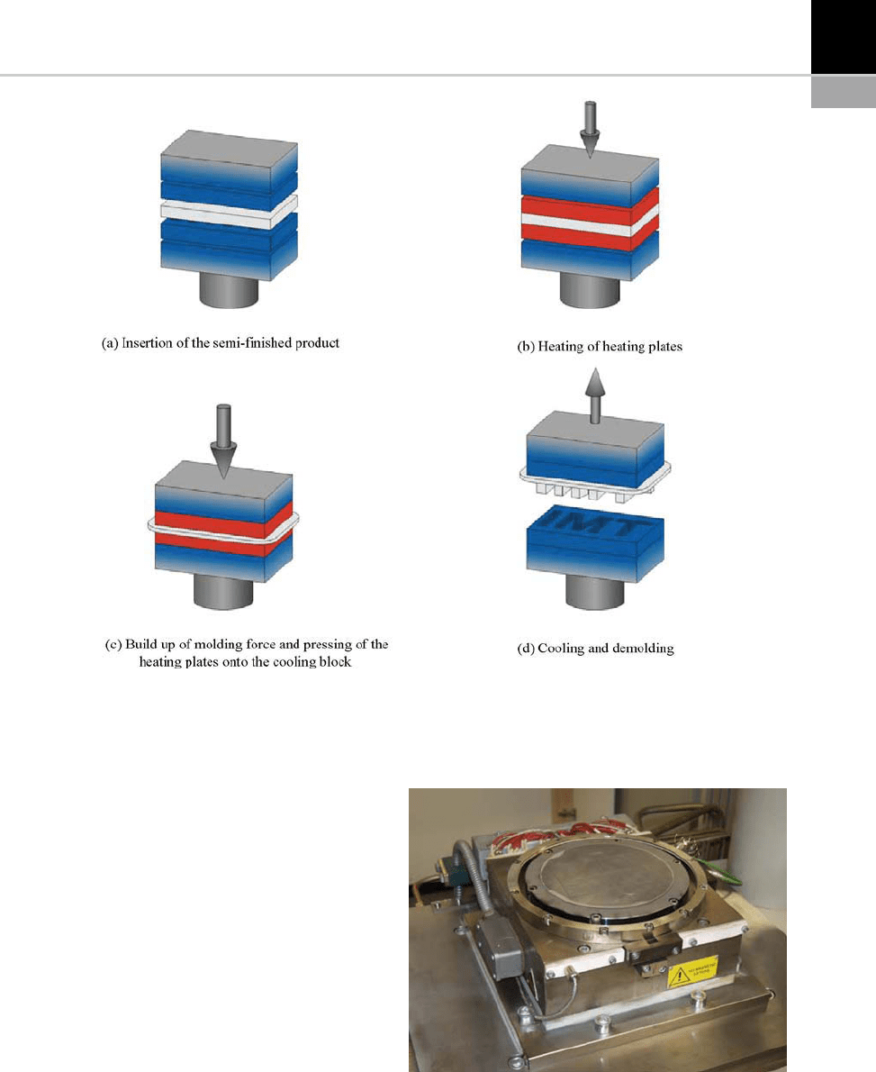
The functioning of this tool is illustrated in
Fig. 5-15. To reduce the heated masses by the
largest possible extent, the hot and cold areas of
the tool are separated thermally. Hence, such a
tool is divided into a heating plate and a so-called
cooling block (Fig. 5-15). In the basic state of the
tool, both functional units are insulated thermally
by an air gap produced with the help of springs
(Fig. 5-15(a)). This air gap is retained when melt-
ing the polymer. The contact force is generated by
the springs only (Fig. 5-15(b)). Due to thermal
insulation, the relatively thin heating plate and
the mold insert can be heated rapidly. In the dis-
placement- and force-controlled embossing pro-
cess, the molding force presses the heating plate
onto the massive cooling block, which results in a
mechanically stable set-up, by means of which
homogeneously thin residual layers may be pro-
duced even on large areas (Fig. 5-15(c)). As soon
as the heating plate is in contact with the cooling
block, heat is removed from the heating plate to
the comparably large and permanently cooled
cooling block. As the cooling block acts like a heat
sink, the heating plate and the mold insert can be
cooled down rapidly. Subsequently, the compo-
nents can be demolded (Fig. 5-15(d)). Except for
the vacuum chamber, the tool halves are designed
symmetrically and consist of a water-cooled cool-
ing block and a heating plate each. The heating
plate is lifted off the cooling block by prestressed
disc spring packages. Mold inserts of 250 mm in
diameter can be fixed onto the heating plate, and
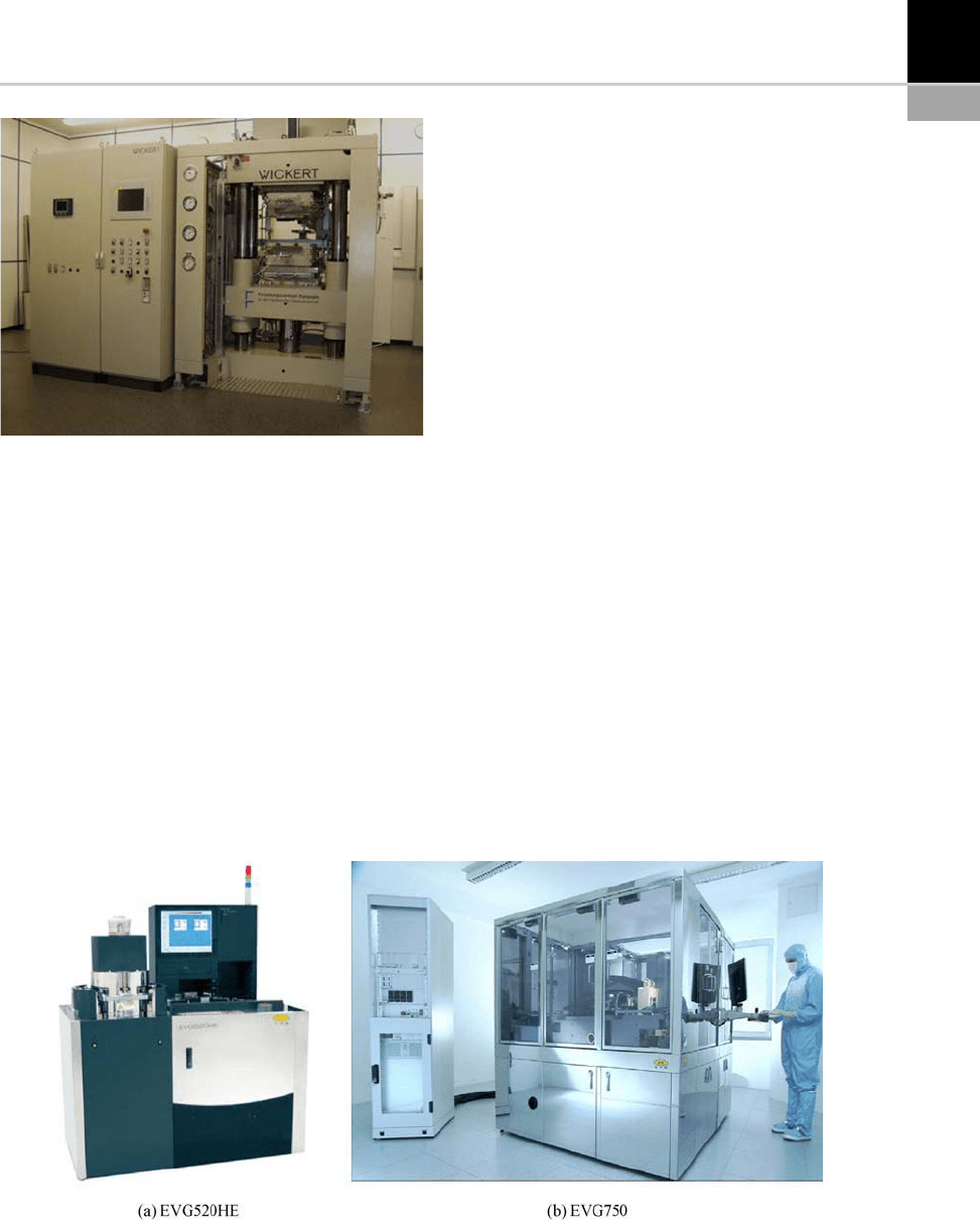
FIGURE 5-12 Hot embossing machine Wickert WMP1000.
FIGURE 5-13 Nano-imprint machine EVG520HE and EVG750.
CHAPTER 5 Hot Embossing 81
the maximum molding temperature is 300
C. In
this tool, the heating plate can be clamped to the
cooling block using a magnetic clamping system.
A tolerance-free opening movement of the hot
embossing machine thus allows for offset-free
demolding. As in conventional hot embossing
tools, substrate plates roughened by lapping or
sand blasting may be used for demolding. The
demonstration tool is presented in Fig. 5-16.
For precise temperature control, the heating
plates of the basic tool are divided into four zones
each, which are controlled separately and may be
set to various temperatures. In this way, a highly
homogeneous temperature distribution can be
achieved in the mold insert. In the hot embossing
process, three different temperat ures can be input
for each tool half: the molding temperature is the
temperature to which the heating plates are
heated, while the embossing temperature is the
temperature at which the embossing force starts
to build up. At the demolding temperature,
demolding of the embossed component starts.
The molding temperature is measured directly in
the individual zones of the heating plates, and the
embossing and demolding temperatures are mea-
sured in the mold insert and substrate plate,
respectively. As the mold insert cools quickly
when the embossing force is generated, it may
be reasonable to select a molding temperature
far above the embossing temperature. As a result
of the thermal inertia of the heating plate and the
cooling block, cooling of the polymer melt is then
slowed slightly: this allows the fabrication of very
thin components of low stress.
The heating concept based on a spring was also
implemented by Schift et al. [18] for the molding
of wafer-type substrates. A clamped stack of the
stamp and substrate was preassembled in an align-
ment system, and it was not in contact with the
heating plate, under action of the spring system.
The gap was closed by the acting of force, pressing
the stack onto the heating plate. After embossing,
the force was set to a low value which results in
the separation of the stack from the heating plate
under action of the springs. The molded part is
cooled and can be demolded manually.
FIGURE 5-14 Schematic view of a basic molding tool with reduced thermal mass.
82 CHAPTER 5 Hot Embossing
Micro-structured Mold Inserts
For every replication process a mold or so-called
master is necessary to copy the structures of the
mold into a molding material. The mold is split
into the tool and the mold insert with the micro-
structured surface. In theory every micro-struc-
tured surface can be used as a mold insert. A
precondition is that the mold material and the
micro-structures will withstand the temperature
and mechanical load during molding. Neverthe-
less, for successful molding, and especially
demolding, the mold insert has to fulfill the fol-
lowing requirements:
*
The yield stress of the mold material at the
maximum molding temperature has to be
FIGURE 5-15 Schematic view of the process steps of hot embossing with the basic molding tool.
FIGURE 5-16 Lower half of a basic molding tool with a
moldable surface area of up to 250 mm diameter.
CHAPTER 5 Hot Embossing 83
significantly higher than the stress effect ed by
the molding force.
*
To avoid any bending and to ensure the greatest
possible evenness of the mold, the residual
stress inside the mold, caused by the fabrication
process, should be reduced to a minimum.
*
The mold material should show chemical resis-
tance against the polymer.
*
There should be a high heat conductivity of the
mold material to reduce the heating and cooling
times.
*
For cost effectiveness the lifetime of the mold
should be extende d over many cycles.
*
To support successful demolding, the surface
roughness, especially of vertical sidewalls,
should be reduced to an unavoidable minimum.
*
Demolding angles are advantageous because
they facilita te demolding. In contrast, under-
cuts prevent the successful demolding of
micro-structures. Even small undercuts in the
sub-micron range can increase de molding
forces significantly.
Regarding the requirements, especially the
requirement of high yield stress, it is obvious that
mold inserts, fabricated in metals, are well suited.
The technique of micro-structuring of metals is
therefore essential for mold fabrication, but also
glass or polymers like UV-transparent PDMS or
high temperature resistant PEEK can be used for
selected replication tasks. Nevertheless, regarding
the lifetime of a mold insert, high stiffness molds
fabricated from metals are widel y used for repli-
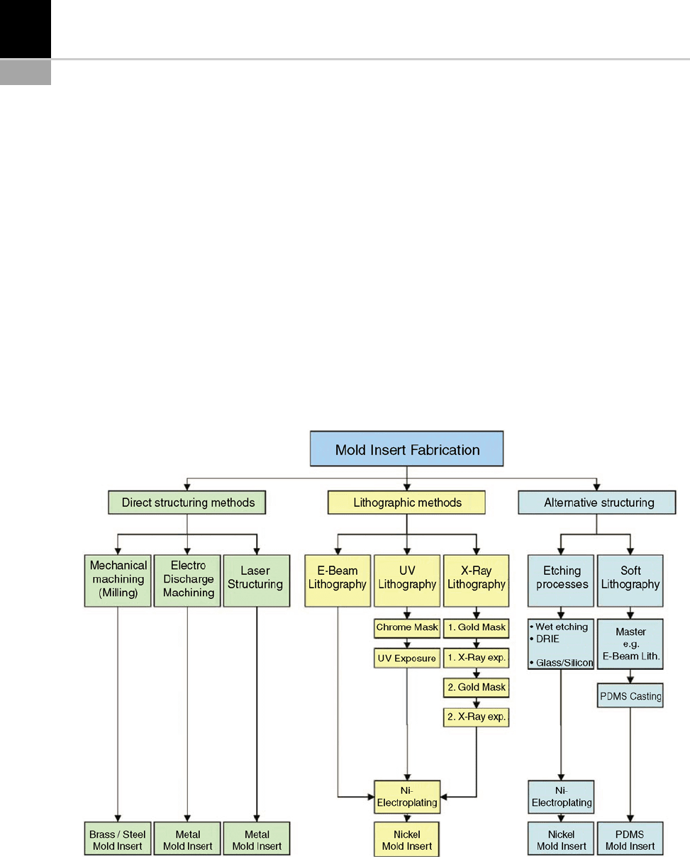
cation. An overview of the different mold fabri-
cation processes is shown in Fig. 5-17.
The structuring processes can be split into two
groups: direct structuring methods like mechani-
cal machining, electric discharge machining
(EDM) or laser structuring [19]; and lithographic
methods like E-beam lithography and UV-lithog-
raphy. For structures with high aspect ratios,
FIGURE 5-17 Overview of the mold fabrication processes.
84 CHAPTER 5 Hot Embossing
X-ray lithography is also used to structure the
mold inserts. All lithographic processes require
the step of electroforming to obtain a metal mold
insert. Each structuring method has different
characteristics and is therefore suitable for differ-
ent kinds of applications.
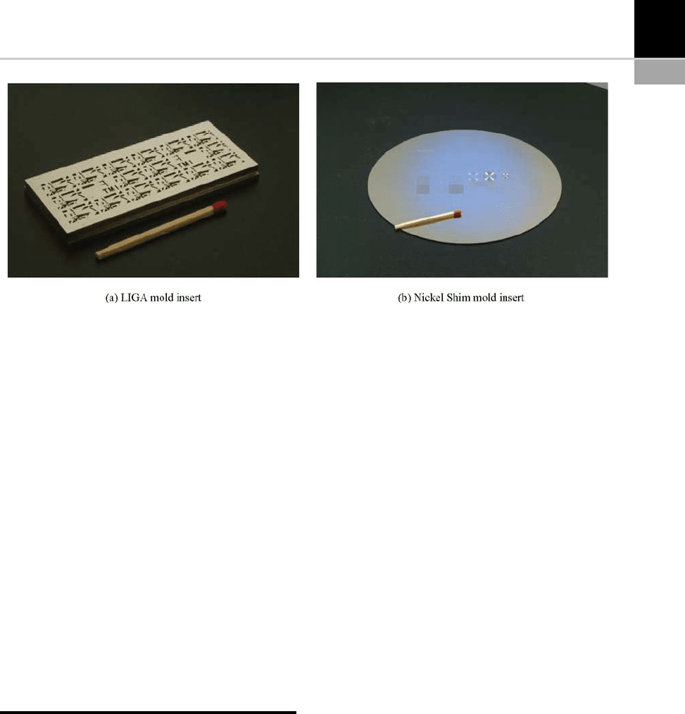
Representative of the large number of suitable
mold inserts are two electroplated mold inserts
shown in Fig. 5-18: a typical LIGA mold insert
with high aspect ratio structures with dimensions
of 28 66 mm
2
and a thickness of 5 mm and as
an alternative for larger structured areas a 4 inch
nickel shim mold insert with a typical thickness of
approximately 300 up to 500 mm.
The height of the structures is 750 mm. Nickel
shims are characterized by a thickness in the range
of several hundred micrometers and are well suited
for the replication of structures with low aspect
ratios on large areas, typically 4 or 6 inches.
APPLICATIONS
This section presents some applications where hot
embossing plays an important role for their fabri-
cation.
Micro-optical Devices
Micro-optical devices are one of the main appli-
cations in micro-system technology. The devices
that can be replicated by hot embossing are
manifold, beginning at micro-optical compo-
nents like lenses, mirrors, optical benches or
waveguides, up to micro-systems like micro-
spectrometers, DFB-laser systems, optical
switches, fiber connectors, photonic crystals or
anti-reflection films [20–21].Becauseofthe
requirements regarding structure sizes, surface
quality and accuracy of lateral distances, the
mold inserts for hot embossing are typically fab-
ricated by lithographic processes.
Optical Waveguides. For optical interconnec-
tion the replication of polymeric waveguides
opens a new field of applications. Depending
on the application, monomode or multimode
waveguides with different sizes are required,
beginning with lateral dimensions of approxi-
mately 6 mm [22] up to 500 mm [23]. Suffici ent
for most applications is an aspect ratio in the
vicinity of unity, but typically a guiding path
over several millimeters or c entimetres is desired.
The design refers typically to free -standing rect-
angular shapes without any additional support-
ing structures, which makes it necessary to
reduce internal stress inside the structures to
avoid any deformation of the shape of the wave-
guides. Several techniques allow the modifica-
tion of the refractive index of the material, for
example the UV-radiation of PMMA, which
makes this m aterial suitable for the replication
of waveguides. Representative for a variety
of polymer waveguides, replicated rectangular
FIGURE 5-18 Electroplated LIGA mold insert, structured by X-ray lithography.
CHAPTER 5 Hot Embossing 85
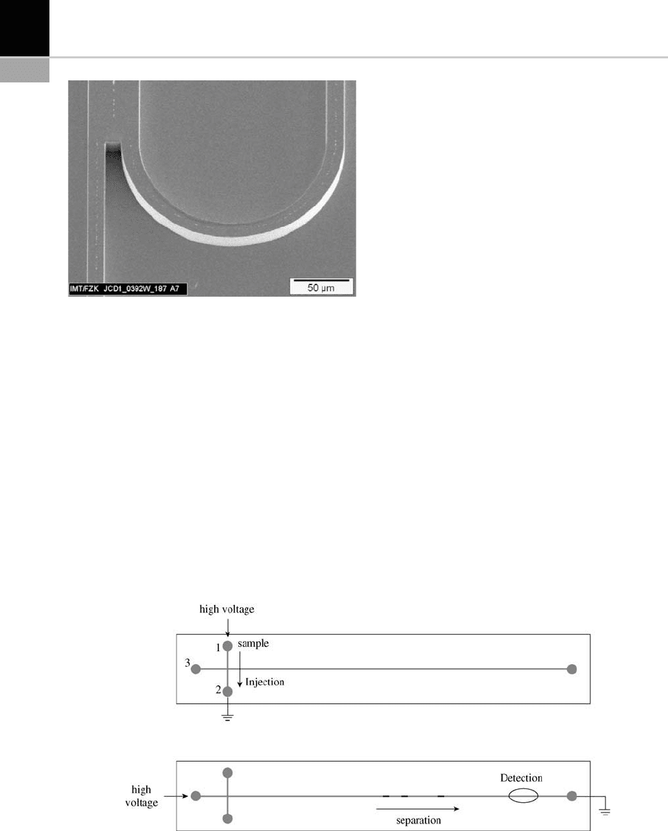
waveguides and further optical splitters are pre-
sented in Fig. 5-19.
The electroplated nickel shim mold was fabri-
cated by UV-lithography and replicated into
PMMA. The refractive index of the molded wave-
guides was modified after replication by UV-
radiation. The basic optical waveguide elements
allow further the development of interactions
between waveguides for subsequent applications
Micro-fluidic Devices
Micro-fluidic systems are part of life science tech-
nology and diagnostic and therapeutic biomedical
engineering. Passive micro-components like cap-
illary micro-channel structures and so-called
wells, reservoir areas or miniaturized sample
chambers can be part of micro-total analysis sys-
tems or lab-on-a-chip systems [24]. Representa-
tive for passive micro-fluidic systems are, for
example, capillary electrophoresis chips. Active
micro-fluidic components like pumping systems
or valve systems are mostly part of complex total
analysis systems.
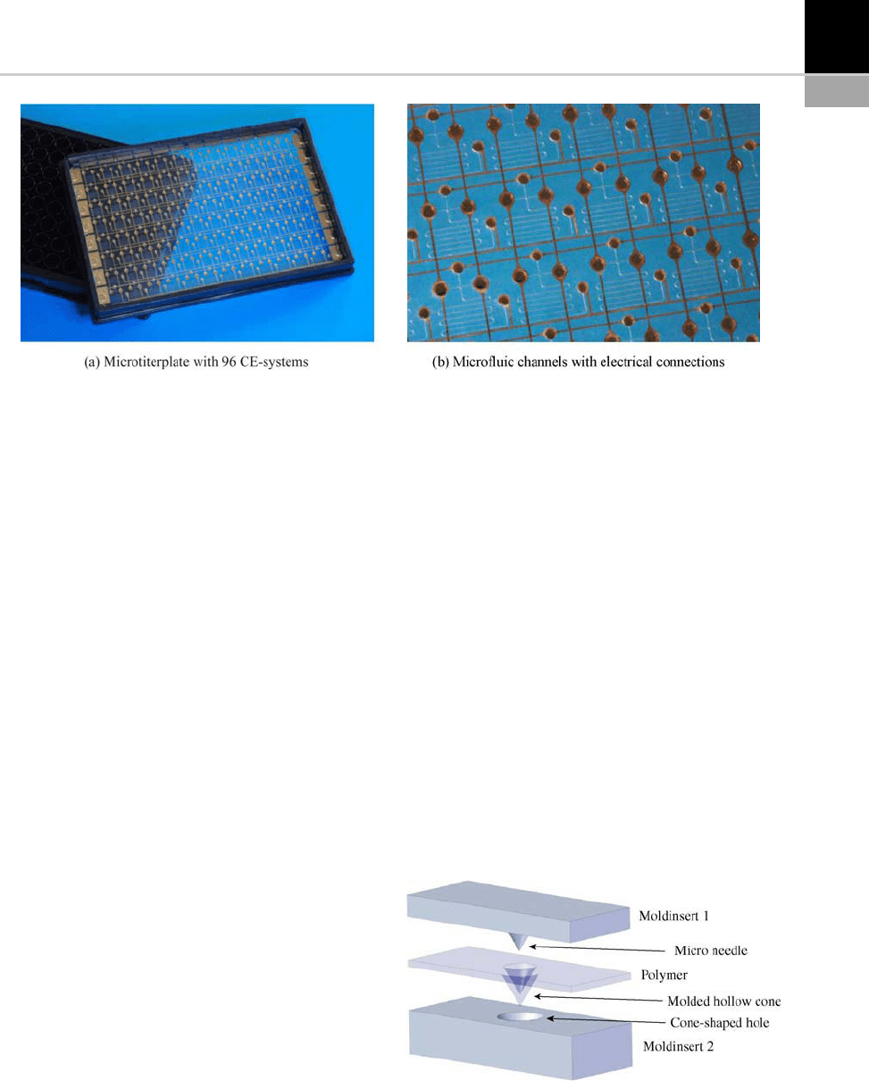
Capillary Analysis Systems. The functioning of
a capillary electrophoresis system can be
explained principally by Fig. 5-20. The system
consists of two intersecting micro-channels with
wells at the beginning (buffer) and at the end
(waste). The first shorter channels will contain
the sample material which should be analyzed,
the longer channels contain a buffer solution. To
achieve a flow an injection of the sample fluid into
the buffer fluid is made at the intersection point; a
difference in potential has to be obtained by elec-
trodes integrated in the wells. By electric switch-
ing the sample volume located in the intersection
area can be injected into the longer separation
channel. In this channel the plug is separated into
its components, depending on molecule size and
electric charge [25]. Characteristic for micro-flu-
idic structures are grooves typically with an aspect
ratio in the vicinity of unity and a flow path of up
to several centimeters which can be arranged in a
FIGURE 5-19 Molded optical waveguides with a cross-
section and height of approximately 6 mm [22].
FIGURE 5-20 Principle of a capillary electrophoresis system.
86 CHAPTER 5 Hot Embossing
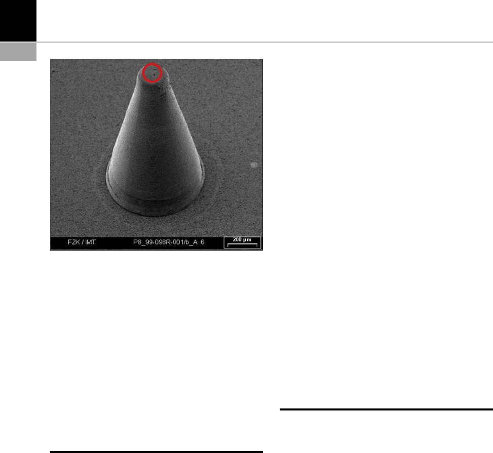
shape of a meander to achieve compact systems.
For easy handling of these struc tures it is recom-
mended to arrange such CE systems onto stan-
dardized platforms, for example microtiterplates
with an area of 125 mm 85 mm. On this area,
for example, 96 CE syst ems could be integrated
(Fig. 5-21).
The principle refers to an intersection of two
micro-channels where a small volume of the sam-
ple fluid is injected into the long fluid channel
with a buffer fluid inside. During the flow the
sample volume will be separated into its compo-
nents, which can be detected at the end of the flow
path. The injection and the flow are supported by
a high voltage differe nce be tween the buffer and
the waste with electrical connections.
Micro-needles
Another application for the hot embossing tech-
nique is an example of a medical technique, in
particular in drug delivery. Micro-needles are
one of the minimal invasive drug delivery systems
entering the body through the skin. Therefore the
outer layer of the skin (stratum corneu m) with a
typically thickness in a range between 10 and
20 mm has to be disrupted. The thickness of this
layer determines the minimum height of the nee-
dles. The biocompatibility of selected polymers
and the fabrication of an array of micro-needles
for the drug delivery make this application well
suited for polymer replication processes. One of
the requirements is a hollow needle which makes
it necessary to integrate a fluid channel inside the
polymer needles.
A suitable fabrication method is the replication
of micro needles by double-sided, positioned hot
embossing. In this case a cone shaped needle on
the one side hits a cone shaped hole in the
other side of a two-sided molding mold insert
(Fig. 5-22). The ach ievable accuracy regarding
the homogeneous thickness of the sidewalls
depends here on the o verlay accuracy of both
mold halves. The advantage of this method is
that only a thin residual l ayer on the tip of the
cone has to be disrupted. This can be done easily,
for example, by laser structuring. The fabrica-
tion of the mold inserts, the positive cone and
the negative cone-shaped hole can be done by
mechanical machining.
FIGURE 5-21 Microtiterplate with 96 CE systems [24,25].
FIGURE 5-22 Double-sided molding of micro-needles.
CHAPTER 5 Hot Embossing 87
To achieve hollow cone-shaped needles dou-
ble-sided positioned molding of a cone-shaped
needle into a cone-shaped hole is required.
Finally, the residual layer of the needle has to
be eliminated. In this case the residual layer is
beside the carrier layer of the needle, also located
in the tip of the cone. To achieve a fluid channel
through the needle, the residual layer has to be
removed. A molded micro-needle with a fine hole
in the tip is shown in Fig. 5-23.
THE OUTLOOK
The examples presented above are only part of
a pool of applications, but they underline the
relevance of the hot embossing or thermal
nano-imprint process as an established r epli-
cation technology. Further developments in
hot embossing and nano-imprinting will be sup-
ported by new applications, e specially if large
series are required. Here the kind of automation
and standardization of, e.g., molding formats
will also help to establish this technology in
the industry as replication technology. Espe-
cially, the cycle times have to be minimized in
future, which corresponds to an efficient heat-
ing and cooling system. Optimized molding
tools are therefore a key issue for cost-effective
molding. In combination with already well-
established handling systems in macroscopic
processing the process times can be minimized
and hot embossing can be established as an
industrial replication technology. A cost-effec-
tive replication also requires large molding
areas. These molding areas correspond to the
fabrication methods of the mold inserts which
are limited individually. To overcome these lim-
its, molding tools with multiple mold inserts
can be used. These aspects are mainly in the
foreground of interest for a cost-effective use
of hot embossing. Independently of the poten-
tial to optimize the cost effectiveness, hot
embossing will stil l be a well-suited process
for the first replications of prototypes. In this
case the f uture may shift the replication to
structures with smaller structure sizes in the
nano-range in combination with high aspect
ratios, e.g. larger than 5. Further, those struc-
tures will be replicated over large areas such as
8 inches or more. Nevertheless, all replication
processes are inspired by the requirements of
the further applications and these applications
will finally determine the structure sizes, the
molding areas and the kind of automation.
REFERENCES
[1] H. Becker, C. G
€
artner, Polymer microfabrication
technologies for microfluidic systems, Anal. Bioanal.
Chem. 390 (2008) 89–111.
[2] H. Becker, U. Heim, Hot embossing as a method for
the fabrication of polymer high aspect ratio struc-
tures, Sensors and Actuators 83 (2000) 130–135.
[3]M.Heckele,W.Bacher,K.D.Mueller,Hot
embossing–the moulding technique for plastic
microstructures, Microsy stem Technologies 4
(1998) 122–124.
[4] M. Heckele, W.K. Schomburg, Review on micro
moulding of thermoplastic polymers, J. of Microme-
chanics and Microengineering 14 (2004) R1–R14.
[5] R. Bartolini, W. Hannan, D. Karlsons, M. Lurie,
Embossed hologram motion pictures for television
playback, Applied Optics 9 (10) (1970) 2283–
2290.
[6] M.T. Gale, J. Kane, K. Knop, Zod images: emboss-
able surface-relief structures for color and black-and-
white reproduction, J. of Applied Photographic
Engineering 4 (2) (1978) 41–47.
FIGURE 5-23 Molded micro-needles with a through-hole
on top of the cone-shaped needle.
88 CHAPTER 5 Hot Embossing

[7] E.W. Becker, W. Ehrfeld, P. Hagmann, A. Maner, D.
M€unchmeyer, Fabrication of microstructures with
high aspect ratios and great structural heights by syn-
chrotron radiation lithography, galvanoforming and
plastic moulding (ligaprocess), Microelectron. Eng 4
(1986) 3556.
[8] M. Harmening, W. Bacher, P. Bley, A. El-Kholi,
H. Kalb, B. Kowanz, W. Menz, A. Michel and
J. Mohr, Moulding of three-dimensional microstruc-
tures by the liga process. In Proc. MEMS’ 92, Tra-
vem
€
unde, Germany, p. 202. IEEE (1992).
[9] Jenoptik Mikrotechnik, http://www.jo-mt.de (2008).
[10] Wickert Press, http://www.wickert-presstech.de
(2008).
[11] Fresnel Optics, http://www.fresnel-optics.de (2008).
[12] K.D. Mueller, Herstellung von beweglichen metal-
lischen Mikrostrukturen auf Siliziumwafern, Sci-
entific report FZKA 6254. Forschungszentrum
Karlsruhe (1999).
[13] Ch. Mehne, Grossformatige Abformung mikrostruk-
turierter Formeinstze durch Heisspr
€
agen, PhD thesis,
University of Karlsruhe, Institute for Microstructure
Technology (2007).
[14] B. Rapp, M. Worgull, M. Heckele, A.E. Guber,
Mikro-Heissstanzen-Erzeugung von Durchloch-
strukturen in ebenen Kunststoffsubstraten, In Con-
ference in Microsystem Technology, Freiburg i. Br,
Germany (2005).
[15] H. Tan, A. Gilbertson, S.Y. Chou, Roller nanoim-
print lithography, J. Vac. Sci. Technol. B 16 (6)
(1998) 3926–3928.
[16] EVG, http://www.EVGroup.com (2008).
[17] Ch. Schaefer, S. Farrens, T. Glinser, P. Lindner,
N. Roos, State of the art automated nanoimprinting
of polymers and its challenges, In 7th International
Conference on the Commercialization of Micro and
Nano Systems (COMS) (September 8–12, 2002).
[18] H. Schift, S. Bellini, J. Gobrecht, F. Reuther,
M. Kubenz, M.B. Mikkelsen, K. Vogelsang, Fast
heating and cooling in nanoimprint using a spring-
loaded adapter in a preheated press, Microelectronic
Engineering 84 (2007) 932–936.
[19] J. Fleischer, J. Kotschenreuther, The manufacturing
of micro moulds by conventional and energy-assisted
processes, Int. J. Adv. Manuf. Technol(2006).
[20] C.J. Ting, M.C. Huang, H.Y. Tsai, C.P. Chou, C.C.
Fu, Low cost fabrication of large-area anti-reflection
films from polymer by nanoimprint/hot-embossing
technology, Nanotechnology 19 (2008) 1–5.
[21] J. Seekamp, S. Zankovych, A.H. Helfer, P. Maury,
C.M. Sotomayor Torres, G. B
€
ottger, C. Liguda, M.
Eich, B. Heidari, L. Montelius, J. Ahopelto, Nanoim-
printed passive optical devices, Nanotechnology 13
(2002) 581–586.
[22] M. Bruendel, Herstellung photonischer Komponen-
ten durch Heisspr
€
agen und UV-induzierte Brechzahl-
modifikation von PMMA, PhD thesis, University of
Karlsruhe (TH), Institute for Microstructure Tech-
nology (2008).
[23] H. Mizuno, O. Sugihara, T. Kaino, N. Okamoto, M.
Hosino, Low-loss polymeric optical waveguides with
large cores fabricated by hot embossing, Optics
Letters 28 (23) (2003) 2378–2380.
[24] A.E. Guber, M. Heckele, D. Herrmann, A. Muslija,
V. Saile, L. Eichhorn, T. Gietzelt, W. Hoffmann, P.C.
Hauser, J. Tanyanyiwa, A. Gerlach, N. Gottschlich,
G. Knebel, Microfluidic lab-on-a-chip systems based
on polymers-fabrication and application, Chemical
Engineering J 101 (2004) 447–453.
[25] A. Gerlach, G. Knebel, A.E. Guber, M. Heckele,
D. Herrmann, A. Muslija, Th. Schaller, Microfabri-
cation of single-use plastic microfluidic devices for
high-throughput screening and DNA analysis,
Microsystem Technologies (2002) 265–268.
CHAPTER 5 Hot Embossing 89

6
Micro-Injection-Molding
Guido Tosello and Hans Nørgaard Hansen
INTRODUCTION
The essential condition for the marke t success of
micro-systems is the cost-effective production of
micro-structures on a large scale. In recent years
plastic molding techniques such as injection mold-
ing, which is a suitable process for medium- and
large-scale fabrication, have been adapted for the
necessities of micro-components fabrication.
Injection molding is a process technology that
has been well established in the production of
polymer parts in the macro-dimensional range
for decades. Therefore, vast know- how and
machine technology is available to be made use
of in micro-injection molding as well.
Moreover, the fabrication costs of mol ded
micro-parts are only slightly affected by the com-
plexity of the design. Once a mol d insert has been
made, several thousands parts can be molded with
little effort. The cost of raw material in most cases
is negligibly low, because only small material
quantities are required for micro-components.
Therefore, parts fabricated by micro-injection
molding, even from high end materials, are suit-
able for applications requiring low cost and dis-
posable components [1]. The result is that plastic
products manufactured by micro-injection mold-
ing have made successful entry into the market. In
fact, peculiar characteristics such as production
capability, disposability, biocompatibility, opti-
cal properties, just to mention a few, pose plastics
as the best choice for numerous micro-products.
Fields of application of micro-molded products
are: micro-optics (waveguides, micro-lenses,
fiber connectors), micro-mechanics (micro-gears,
micro-actuators, micro-pumps, micro-switches),
information storage and data carrier devices
(CDs, DVDs, sensor discs), micro-fluidic systems
(blood analysis, DNA analysis), medical technol-
ogy (hearing aid, components for minimal inva-
sive surgery).
When downscaling systems, products, and
their components, the limits of conventional
manufacturing techniques are reached. This initi-
ated the improvement of conventional techniques
and the further development of new ones, as in the
case of the micro-injection molding process. Lat-
eral dimensions in the micrometer range, struc-
tural details in the sub-micrometer dimensional
level and high aspect ratio (aspect ratio = depth/
width) of 10 and above are achieved. There are a
variety of applications already known for the
micro-molding of thermoplastic polymers an d
many more are expected to arise in the future.
MICRO-INJECTION MOLDIN G
SCENARIO
Injection molding is one of the most versatile and
important operations for the mass production of
complex plastic parts. Injection-molded parts
typically have good dimensional tolerance and
require almost no finishing and assembl y opera-
tions. In addition to thermoplastics and thermo-
sets, the process is also being extended to such
materials as fibers, ceramics, and powder materi-
als, with polymer as binders. Among all the
polymer-processing methods, injection molding
accounts for 32% by weight of all the polymeric
CHAPTER
90
