Power electronic handbook
Подождите немного. Документ загружается.

13 DC–DC Converters 247
S
V
S
D
R
L
E
+
v
O
–
(a)
(b)
0
v
O
V
S
0DTT t
i
O
t
FIGURE 13.2 DC chopper with RLE load: (a) circuit diagram and
(b) waveforms.
V
S
+
v
O
–
L
D
S
Load
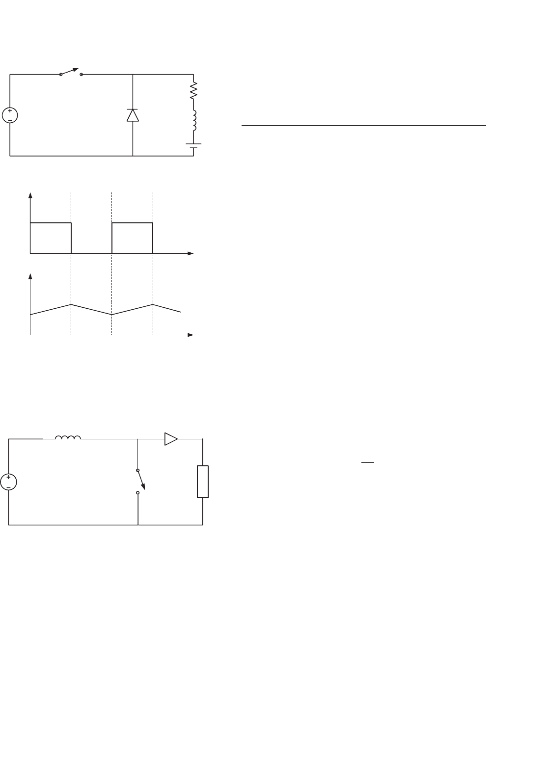
FIGURE 13.3 The dc step-up chopper.
The dc choppers can also provide peak output voltages
higher than the input voltage. Such a step-up configuration is
presented in Fig. 13.3. It consists of dc input source V
S
, induc-
tor L connected in series with the source, switch S connecting
the inductor to ground, and a series combination of diode D
and load. If the switch operates with a duty ratio D, the output
voltage is a series of pulses of duration (1−D)T and amplitude
V
S
/(1 −D). Neglecting losses, the average value of the output
voltage is V
S
. To obtain an average value of the output voltage
greater than V
S
, a capacitor must be connected in parallel with
the load. This results in a topology of a boost dc–dc converter
that is described in Section 13.4.
13.3 Step-down (Buck) Converter
13.3.1 Basic Converter
The step-down dc–dc converter, commonly known as a buck
converter, is shown in Fig. 13.4a. It consists of dc input voltage
source V
S
, controlled switch S, diode D, filter inductor L,
filter capacitor C, and load resistance R. Typical waveforms
in the converter are shown in Fig. 13.4b under assumption
that the inductor current is always positive. The state of the
converter in which the inductor current is never zero for
any period of time is called the continuous conduction mode
(CCM). It can be seen from the circuit that when the switch S
is commanded to the on state, the diode D is reverse biased.
When the switch S is off, the diode conducts to support an
uninterrupted current in the inductor.
The relationship among the input voltage, output voltage,
and the switch duty ratio D can be derived, for instance,
from the inductor voltage v
L
waveform (see Fig. 13.4b).
According to Faraday’s law, the inductor volt–second product
over a period of steady-state operation is zero. For the buck
converter
(V
S
−V
O
)DT =−V
O
(1 −D)T (13.3)
Hence, the dc voltage transfer function, defined as the ratio of
the output voltage to the input voltage, is
M
V
≡
V
O
V
S
= D (13.4)
It can be seen from Eq. (13.4) that the output voltage is always
smaller than the input voltage.
The dc–dc converters can operate in two distinct modes
with respect to the inductor current i
L
. Figure 13.4b depicts
the CCM in which the inductor current is always greater than
zero. When the average value of the input current is low
(high R) and/or the switching frequency f is low, the con-
verter may enter the discontinuous conduction mode (DCM).
In the DCM, the inductor current is zero during a portion
of the switching period. The CCM is preferred for high effi-
ciency and good utilization of semiconductor switches and
passive components. The DCM may be used in applications
with special control requirements, since the dynamic order of
the converter is reduced (the energy stored in the inductor is
zero at the beginning and at the end of each switching period).
It is uncommon to mix these two operating modes because of
different control algorithms. For the buck converter, the value
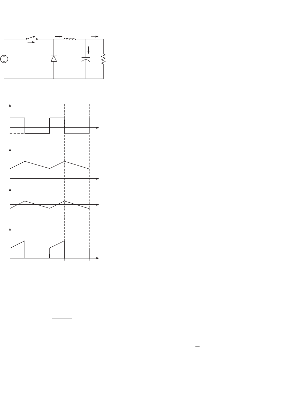
248 D. Czarkowski
0
t
v
L
V
S
–V
O
0
t
i
L
V
S
+
V
O
–
L
+v
L
–
S
D
C
R
I
O
i
L
i
S
i
C
(a)
–V
O
0
t
i
C
i
S
0DT T 2T
t
(b)
FIGURE 13.4 Buck converter: (a) circuit diagram and (b) waveforms.
of the filter inductance that determines the boundary between
CCM and DCM is given by
L
b
=
(1 −D)R
2f
(13.5)
For typical values of D = 0.5, R = 10 , and f = 100 kHz, the
boundary is L
b
= 25 µH. For L > L
b
, the converter operates
in the CCM.
The filter inductor current i
L
in the CCM consists of a dc
component I
O
with a superimposed triangular ac component.
Almost all of this ac component flows through the filter capac-
itor as a current i
c
. Current i
c
causes a small voltage ripple
across the dc output voltage V
O
. To limit the peak-to-peak
value of the ripple voltage below certain value V
r
, the filter
capacitance C must be greater than
C
min
=
(1 −D) V
O
8V
r
Lf
2
(13.6)
At D = 0.5, V
r
/V
O
= 1%, L = 25 µH, and f = 100 kHz,
the minimum capacitance is C
min
= 25 µF.
Equations (13.5) and (13.6) are the key design equations for
the buck converter. The input and output dc voltages (hence,
the duty ratio D), and the range of load resistance R are usually
determined by preliminary specifications. The designer needs
to determine values of passive components L and C, and of
the switching frequency f. The value of the filter inductor L is
calculated from the CCM/DCM condition using Eq. (13.5).
The value of the filter capacitor C is obtained from the
voltage ripple condition Eq. (13.6). For the compactness and
low conduction losses of a converter, it is desirable to use small
passive components. Equations (13.5) and (13.6) show that it
can be accomplished by using a high switching frequency f. The
switching frequency is limited, however, by the type of semi-
conductor switches used and by switching losses. It should
be also noted that values of L and C may be altered by
effects of parasitic components in the converter, especially
by the equivalent series resistance of the capacitor. The issue
of parasitic components in dc–dc converters is discussed in
Section 13.7.
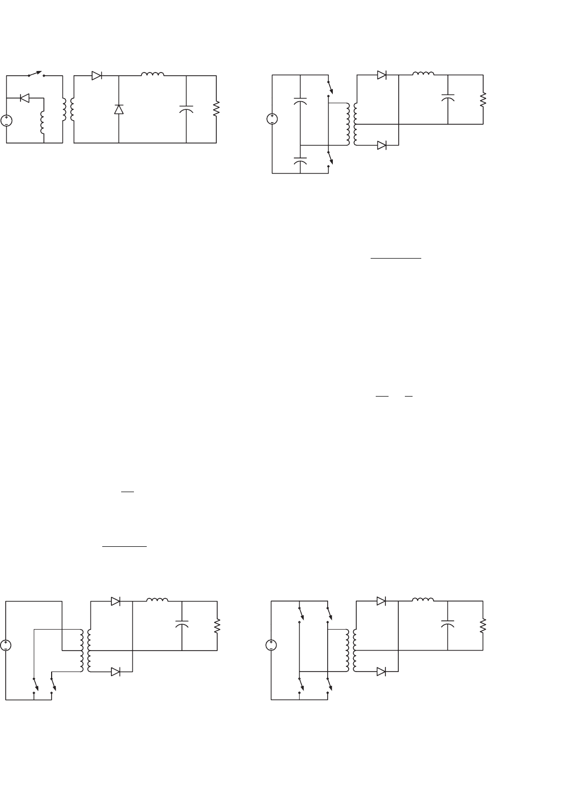
13.3.2 Transformer Versions of Buck Converter
In many dc power supplies, a galvanic isolation between the
dc or ac input and the dc output is required for safety and
reliability. An economical mean of achieving such an isola-
tion is to employ a transformer version of a dc–dc converter.
High-frequency transformers are of a small size and weight and
provide high efficiency. Their turns ratio can be used to addi-
tionally adjust the output voltage level. Among buck-derived
dc–dc converters, the most popular are: forward converter,
push–pull converter, half-bridge converter, and full-bridge
converter.
A. Forward Converter
The circuit diagram of a forward converter is depicted in
Fig. 13.5. When the switch S is on, diode D
1
conducts and
diode D
2
is off. The energy is transferred from the input,
through the transformer, to the output filter. When the switch
is off, the state of diodes D
1
and D
2
is reversed. The dc voltage
transfer function of the forward converter is
M
V
=
D
n
(13.7)
where n = N
1
/N
2
.
13 DC–DC Converters 249
D
3
S
V
S
N
3
N
2
N
1
D
1
D
2
L
C
R
+
V
O
–
··
·
FIGURE 13.5 Forward converter.
In the forward converter, the energy-transfer current flows
through the transformer in one direction. Hence, an additional
winding with diode D
3
is needed to bring the magnetizing
current of the transformer to zero. This prevents transformer
saturation. The turns ratio N
1
/N
3
should be selected in such
a way that the magnetizing current decreases to zero during a
fraction of the time interval when the switch is off.
Equations (13.5) and (13.6) can be used to design the filter
components. The forward converter is very popular for low
power applications. For medium power levels, converters with
bidirectional transformer excitation (push–pull, half-bridge,
and full-bridge) are preferred due to better utilization of
magnetic components.
B. Push–Pull Converter
The PWM dc–dc push–pull converter is shown in Fig. 13.6.
The switches S
1
and S
2
operate shifted in phase by T/2 with the
same duty ratio D. The duty ratio must be smaller than 0.5.
When switch S
1
is on, diode D
1
conducts and diode D
2
is off.
Diode states are reversed when switch S
2
is on. When both con-
trollable switches are off, the diodes are on and share equally
the filter inductor current. The dc voltage transfer function of
the push–pull converter is
M
V
=
2D
n
(13.8)
where n = N
1
/N
2
. The boundary value of the filter inductor is
L
b
=
(1 −2D)R
4f
(13.9)
N
2
N
1
S
1
S
2
V
S
D
1
D
2
L
C
R
+
V
O
–
·
·
·
·
FIGURE 13.6 Push–pull converter.
N
2
N
1
S
1
S
2
V
S
D
1
D
2
L
C
R
+
V
O
–
V
S
/2
V
S
/2
·
··
FIGURE 13.7 Half-bridge converter.
The filter capacitor can be obtained from
C
min
=
(1 −2D)V
O
32V
r
Lf
2
(13.10)
C. Half-bridge Converter
Figure 13.7 shows the dc–dc half-bridge converter. The oper-
ation of the PWM half-bridge converter is similar to that
of the push–pull converter. In comparison to the push–
pull converter, the primary of the transformer is simpli-
fied at the expense of two voltage-sharing input capacitors.
The half-bridge converter dc voltage transfer function is
M
V
≡
V
D
V
S
=
D
n
(13.11)
where D ≤ 0.5. Equations (13.9) and (13.10) apply to the filter
components.
D. Full-bridge Converter
Comparing the PWM dc–dc full-bridge converter of Fig. 13.8
to the half-bridge converter, it can be seen that the input
capacitors have been replaced by two controllable switches.
The controllable switches are operated in pairs. When S
1
and
S
4
are on, voltage V
S
is applied to the primary of the trans-
former and diode D
1
conducts, With S
2
and S
3
on, there is
voltage −V
S
across the primary transformer and diode D
2
N
2
N
1
S
2
S
4
V
S
D
1
D
2
L
C
R
+
V
O
–
S
1
S
3
·
··
FIGURE 13.8 Full-bridge converter.

250 D. Czarkowski
is on. With all controllable switches off, both diodes conduct,
similarly as in the push–pull and half-bridge converters. The
dc voltage transfer function of the full-bridge converter is
M
V
≡
V
O
V
S
=
2D
n
(13.12)
where D ≤ 0.5. Values of filter components can be obtained
from Eqs. (13.9) and (13.10).
It should be stressed that the full-bridge topology is a very
versatile one. With different control algorithms, it is very pop-
ular in dc–ac conversion (square-wave and PWM single-phase
inverters). It is also used in four-quadrant dc drives.
13.4 Step-up (Boost) Converter
Figure 13.9a depicts a step-up or a PWM boost converter. It is
comprised of dc input voltage source V
S
, boost inductor L,
controlled switch S, diode D, filter capacitor C, and load resis-
tance R. The converter waveforms in the CCM are presented in
Fig. 13.9b. When the switch S is in the on state, the current in
the boost inductor increases linearly. The diode D is off at the
time. When the switch S is turned off, the energy stored in the
inductor is released through the diode to the input RC circuit.
Using the Faraday’s law for the boost inductor
V
S
DT = (V
O
−V
S
)(1 −D)T (13.13)
from which the dc voltage transfer function turns out to be
M
V
≡
V
O
V
S
=
1
1 −D
(13.14)
As the name of the converter suggests, the output voltage is
always greater than the input voltage.
The boost converter operates in the CCM for L > L
b
where
L
b
=
(1 −D)
2
DR
2f
(13.15)
For D = 0.5, R = 10 , and f = 100 kHz, the boundary value
of the inductance is L
b
= 6.25 µH.
As shown in Fig. 13.9b, the current supplied to the output
RC circuit is discontinuous. Thus, a larger filter capacitor is
required in comparison to that in the buck-derived converters
to limit the output voltage ripple. The filter capacitor must
provide the output dc current to the load when the diode D
0
t
v
L
V
S
0
t
i
L
V
S
C
R
I
O
i
L
i
C
(a)
V
S
–V
O
0
t
i
S
DT T 2T
(b)
S
L
+v
L
–
i
S
D
i
C
0
t
–I
O
+
V
O
–
FIGURE 13.9 Boost converter: (a) circuit diagram and (b) waveforms.
is off. The minimum value of the filter capacitance that results
in the voltage ripple V
r
is given by
C
min
=
DV
O
V
r
Rf
(13.16)
At D = 0.5, V
r
/V
O
= 1%, R = 10 , and f = 100 kHz, the
minimum capacitance for the boost converter is C
min
= 50 µF.
The boost converter does not have a popular transformer
(isolated) version.
13 DC–DC Converters 251
13.5 Buck–Boost Converter
13.5.1 Basic Converter
A non-isolated (transformerless) topology of the buck–boost
converter is shown in Fig. 13.10a. The converter consists of
dc input voltage source V
S
, controlled switch S, inductor L,
diode D, filter capacitor C, and load resistance R. With the
switch on, the inductor current increases while the diode is
0
t
v
L
V
S
0
t
i
L
V
S
+
V
O
–
C
R
I
O
i
C
(a)
V
O
0
t
i
S
DT T 2T
(b)
i
L
i
S
D
i
C
0
t
–I
O
S
L
+
v
L
–
FIGURE 13.10 Buck–boost converter: (a) circuit diagram and (b)
waveforms.
maintained off. When the switch is turned off, the diode pro-
vides a path for the inductor current. Note the polarity of the
diode which results in its current being drawn from the output.
The buck–boost converter waveforms are depicted in
Fig. 13.10b. The condition of a zero volt–second product for
the inductor in steady state yields
V
S
DT =−V
O
(1 −D)T (13.17)
Hence, the dc voltage transfer function of the buck–boost
converter is
M
V
≡
V
O
V
S
=−
D
1 −D
(13.18)
The output voltage V
O
is negative with respect to the ground.
Its magnitude can be either greater or smaller (equal at D =
0.5) than the input voltage as the converter’s name implies.
The value of the inductor that determines the boundary
between the CCM and DCM is
L
b
=
(1 −D)
2
R
2f
(13.19)
The structure of the output part of the converter is similar
to that of the boost converter (reversed polarities being the
only difference). Thus, the value of the filter capacitor can be
obtained from Eq. (13.16).
13.5.2 Flyback Converter
A PWM flyback converter is a very practical isolated ver-
sion of the buck–boost converter. The circuit of the flyback
converter is presented in Fig. 13.11a. The inductor of the
buck–boost converter has been replaced by a flyback trans-
former. The input dc source V
S
and switch S are connected
in series with the primary transformer. The diode D and the
RC output circuit are connected in series with the secondary
of the flyback transformer. Figure 13.11b shows the converter
with a simple flyback transformer model. The model includes
a magnetizing inductance L
m
and an ideal transformer with
a turns ratio n = N
1
/N
2
. The flyback transformer leakage
inductances and losses are neglected in the model. It should
be noted that leakage inductances, although not important
from the principle of operation point of view, affect adversely
switch and diode transitions. Snubbers are usually required in
flyback converters.
Refer to Fig. 13.11b for the converter operation. When the
switch S is on, the current in the magnetizing inductance
increases linearly. The diode D is off and there is no current
in the ideal transformer windings. When the switch is turned
off, the magnetizing inductance current is diverted into the
ideal transformer, the diode turns on, and the transformed
252 D. Czarkowski
+
V
O
–
C
R
D
S
V
S
V
S
N
2
N
1
(a)
+
V
O
–
C
D
S
N
2
N
1
L
m
(b)
R
·
·
·
·
FIGURE 13.11 Flyback converter: (a) circuit diagram and (b) circuit
with a transformer model showing the magnetizing inductance L
m
.
magnetizing inductance current is supplied to the RC load.
The dc voltage transfer function of the flyback converter is
M
V
≡
V
O
V
S
=
D
n(1 −D)
(13.20)
It differs from the buck–boost converter voltage transfer
function by the turns ratio factor n. A positive sign has
been obtained by an appropriate coupling of the transformer
windings.
Unlike in transformer buck-derived converters, the mag-
netizing inductance L
m
of the flyback transformer is an
important design parameter. The value of the magnetizing
inductance that determines the boundary between the CCM
and DCM is given by
L
mb
=
n
2
(1 −D)
2
R
2f
(13.21)
The value of the filter capacitance can be calculated using
Eq. (13.16).
13.6
`
Cuk Converter
The circuit of the
`
Cuk converter is shown in Fig. 13.12a.
It consists of dc input voltage source V
S
, input inductor L
1
,
controllable switch S, energy transfer capacitor C
1
, diode D,
filter inductor L
2
, filter capacitor C, and load resistance R.
V
S
I
L1
(a)
S
L
1
i
S
C
1
+ v
C1
–
i
C1
D
+
V
O
–
C
R
L
2
I
L2
+
v
S
–
v
C1
v
S
V
S
(b)
i
S
I
L1
+ I
L2
i
C1
I
L1
0
t
–I
L2
0
t
0
t
0 DT T 2T t
FIGURE 13.12
`
Cuk converter: (a) circuit diagram and (b) waveforms.
An important advantage of this topology is a continuous
current at both the input and the output of the converter.
Disadvantages of the
`
Cuk converter include a high number of
reactive components and high current stresses on the switch,
the diode, and the capacitor C
1
. Main waveforms in the con-
verter are presented in Fig. 13.12b. When the switch is on, the
diode is off and the capacitor C
1
is discharged by the inductor
L
2
current. With the switch in the off state, the diode conducts
currents of the inductors L
1
and L
2
whereas capacitor C
1
is
charged by the inductor L
1
current.
To obtain the dc voltage transfer function of the converter,
we shall use the principle that the average current through a
capacitor is zero for steady-state operation. Let us assume that
inductors L
1
and L
2
are large enough that their ripple current
can be neglected. Capacitor C
1
is in steady state if
I
L2
DT = I
L1
(1 −D)T (13.22)

13 DC–DC Converters 253
For a lossless converter
P
S
= V
S
I
L1
=−V
O
I
L2
= P
O
(13.23)
Combining these two equations, the dc voltage transfer
function of the
`
Cuk converter is
M
V
≡
V
O
V
S
=−
D
1 −D
(13.24)
This voltage transfer function is the same as that for the
buck–boost converter.
The boundaries between the CCM and DCM are deter-
mined by
L
b1
=
(1 −D)R
2Df
(13.25)
for L
1
and
L
b2
=
(1 −D)R
2f
(13.26)
for L
2
.
The output part of the
`
Cuk converter is similar to that
of the buck converter. Hence, the expression for the filter
capacitor C is
C
min
=
(1 −D)V
O
8V
r
L
2
f
2
(13.27)
The peak-to-peak ripple voltage in the capacitor C
1
can be
estimated as
V
r1
=
DV
O
C
1
Rf
(13.28)
A transformer (isolated) version of the
`
Cuk converter can
be obtained by splitting capacitor C
1
and inserting a high-
frequency transformer between the split capacitors.
13.7 Effects of Parasitics
The analysis of converters in Sections 13.2 through 13.6 has
been performed under ideal switch, diode, and passive com-
ponent assumptions. Non-idealities or parasitics of practical
devices and components may, however, greatly affect some
performance parameters of dc–dc converters. In this section,
effects of parasitics on output voltage ripple, efficiency, and
voltage transfer function of converters will be illustrated.
A more realistic model of a capacitor than just a
capacitance C, consists of a series connection of capacitance
C and resistance r
C
. The resistance r
C
is called an equiva-
lent series resistance (ESR) of the capacitor and is due to
losses in the dielectric and physical resistance of leads and
connections. Recall Eq. (13.6) which provided a value of the
filter capacitance in a buck converter that limits the peak-to-
peak output voltage ripple to V
r
. The equation was derived
under an assumption that the entire triangular ac component
of the inductor current flows through a capacitance C.Itis,
however, closer to reality to maintain that this triangular com-
ponent flows through a series connection of capacitance C and
resistance r
C
.
The peak-to-peak ripple voltage is independent of the
voltage across the filter capacitor and is determined only by
the ripple voltage of the ESR if the following condition is
satisfied,
C ≥ C
min
= max
1 −D
min
2r
C
f
,
D
max
2r
C
f
(13.29)
If condition (13.29) is satisfied, the peak-to-peak ripple voltage
of the buck and forward converters is
V
r
= r
C
i
Lmax
=
r
C
V
O
(1 −D
min
)
fL
(13.30)
For push–pull, half-bridge, and full-bridge converters,
C ≥ C
min
= max
0.5 −D
min
2r
C
f
,
D
max
2r
C
f
(13.31)
where D
max
≤ 0.5. If condition (13.31) is met, the peak-to-
peak ripple voltage V
r
of these converters is given by
V
r
= r
C
i
Lmax
=
r
C
V
O
(0.5 −D
min
)
fL
(13.32)
Waveforms of voltage across the ESR V
rC
, voltage across
the capacitance V
C
, and total ripple voltage V
r
are depicted
in Fig. 13.13 for three values of the filter capacitances. For the
case of the top graph in Fig. 13.13, the peak-to-peak value
of V
r
is higher than the peak-to-peak value of V
rC
because
C < C
min
. Middle and bottom graphs in Fig. 13.13 show the
waveforms for C = C
min
and C > C
min
, respectively. For both
these cases, the peak-to-peak voltages of V
r
and V
rC
equal to
each other.
Note that when the resistance r
C
sets the ripple voltage V
r
,
the minimum value of inductance L is determined either by the
boundary between the CCM and DCM according to Eq. (13.5)
(buck and forward converters) or Eq. (13.9) (push–pull, half-
bridge, and full-bridge converters), or by the voltage ripple
condition (13.30) or (13.32).
In buck–boost and boost converters, the peak-to-peak
capacitor current I
Cpp
is equal to the peak-to-peak diode
current and is given by
I
Cpp
=
I
O
1 −D
(13.33)
254 D. Czarkowski
V
rC
V
rC
V
rC
V
r
V
r
V
r
V
C
V
C
V
C
–0.08
0.2 0.4 0.6 0.8 10
0.2 0.4 0.6 0.8 10
0.2 0.4 0.6 0.8 10
0
0.04
0.08
–0.04
0
0.04
0.08
–0.04
–0.08
0
0.04
0.08
–0.04
–0.08
ripple voltage (V) ripple voltage (V)ripple voltage (V)
V
t/T
FIGURE 13.13 Voltage ripple waveforms V
rC
, V
C
, and V
r
for a buck
converter at V
O
= 12 V, f = 100 kHz, L = 40 µH, r
C
= 0.05 , and
various values of C: C = 33 µF (top graph), C = C
min
= 65 µF (middle
graph), and C = 100 µF (bottom graph).
under condition that the inductor current ripple is much lower
than the average value of the inductor current. The peak-to-
peak voltage across the ESR is
V
rC
= r
C
I
Cpp
=
r
C
I
O
1 −D
(13.34)
Assuming that the total ripple voltage V
r
is approximately
equal to the sum of the ripple voltages across the ESR and the
capacitance, the maximum value of the peak-to-peak ripple
voltage across the capacitance is
V
Cmax
≈ V
r
−V
rC
(13.35)
Finally, by analogy to Eq. (13.16), when the ESR of the filter
capacitor is taken into account in the boost-type output filter,
the filter capacitance should be greater than
C
min
=
DV
O
V
Cmax
Rf
(13.36)
Parasitic resistances, capacitances, and voltage sources affect
also an energy conversion efficiency of dc–dc converters.
The efficiency η is defined as a ratio of output power to the
input power
η ≡
P
O
P
S
=
V
O
I
O
V
S
I
S
(13.37)
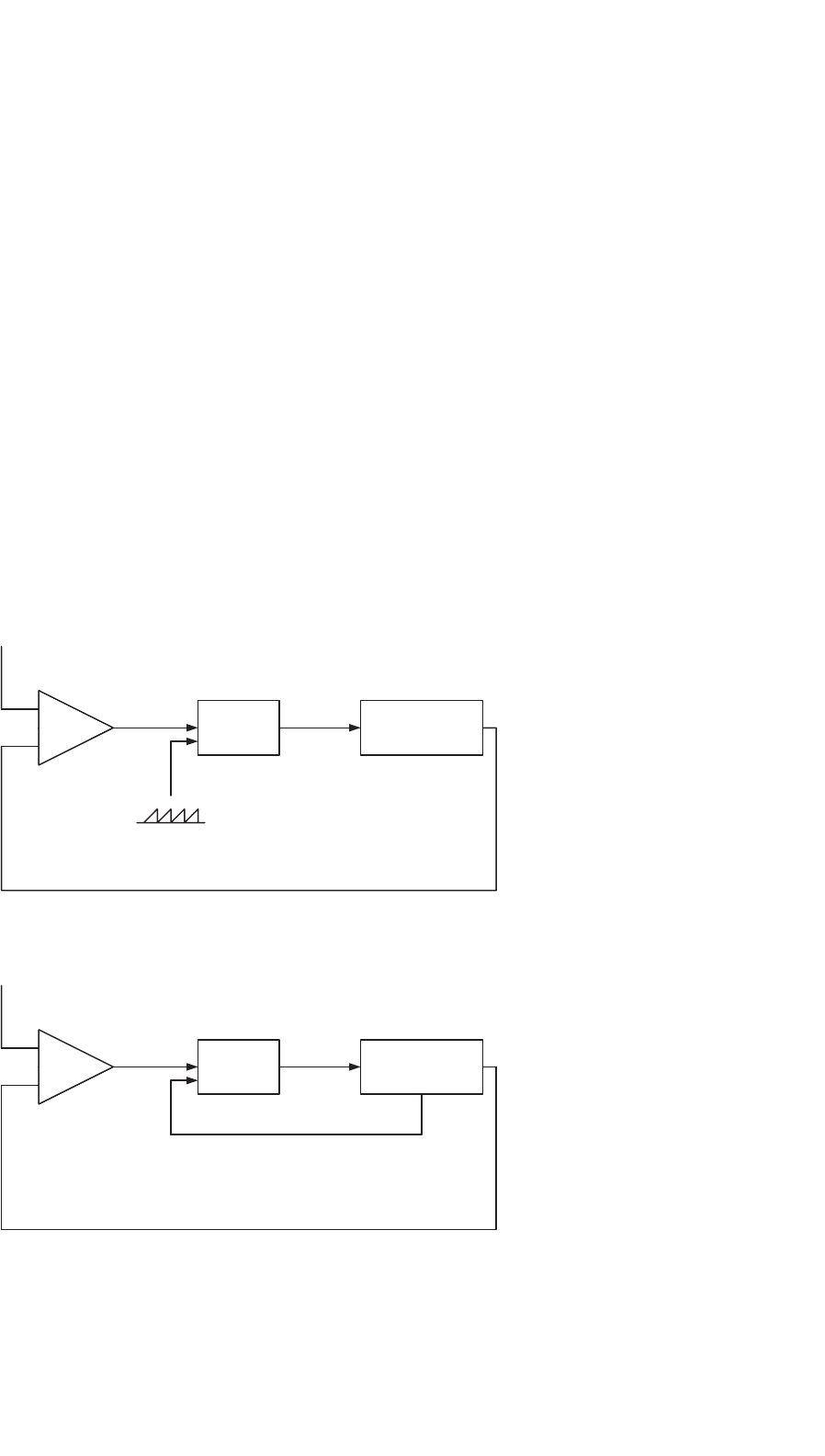
Efficiencies are usually specified in percent. Let us consider the
boot converter as an example. Under low ripple assumption,
the boost converter efficiency can be estimated as
η=
R(1−D)
2
R(1−D)
2
(1+(V
D
/V
O
)+fC
o
R)+r
L
+Dr
S
+(1−D)r
D
+D(1−D)r
C
(13.38)
where V
D
is the forward conduction voltage drop of the diode,
C
o
is the output capacitance of the switch, r
L
is the ESR of the
inductor, and r
D
is the forward on resistance of the diode.
The term fC
o
R in Eq. (13.38) represents switching losses in
the converter. Other terms account for conduction losses.
Losses in a dc–dc converter also contribute to a decrease in
the dc voltage transfer function. The non-ideal dc voltage
transfer function M
Vn
is a product of the ideal one and the
efficiency
M
Vn
= ηM
V
(13.39)
Sample graphs for the boost converter that corre-
spond to Eqs. (13.38) and (13.39) are presented in
Fig. 13.14.
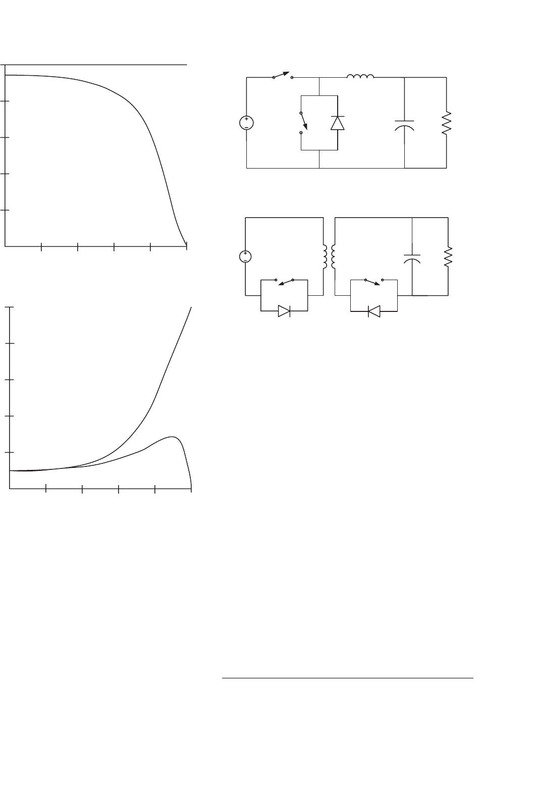
13.8 Synchronous and Bidirectional
Converters
It can be observed in Eq. (13.38) that the forward voltage
of a diode V
D
contributes to a decrease in efficiency. This
contribution is especially significant in low output voltage
power supplies, e.g. 3.3 V power supplies for microprocessors
or power supplies for portable telecommunication equipment.
Even with a Schottky diode, which has V
D
in the range of
0.4 V, the power loss in the diode can easily exceed 10% of
the total power delivered to the load. To reduce conduction
losses in the diode, a low on-resistance switch can be added
in parallel as shown in Fig. 13.15 for a buck converter. The
input switch and the switch parallel to the diode must be
13 DC–DC Converters 255
Efficiency (%)
D
Ideal
100
80
60
0
20
40
0.2 0.4 0.6 0.8 1.0
0 0.2 0.4 0.6 0.8 1.0
Non-ideal
M
V
, M
Vn
D
10
8
6
2
4
Ideal
Non-ideal
(a)
(b)
FIGURE 13.14 Effects of parasitics on characteristics of a boost con-
verter: (a) efficiency and (b) dc voltage transfer function.
turned on and off alternately. The arrangement of Fig. 13.15
is called a synchronous converter or a synchronous rectifier.
Modern low-voltage MOSFETs have on resistances of only sev-
eral milliohms. Hence, a synchronous converter may exhibit
higher efficiency than a conventional one at output currents
as large as tens of amperes. The efficiency is increased at an
expense of more complicated driving circuitry for the switches.
In particular, a special can must be exercised to avoid hav-
ing both switches on at the same time as this would short
the input voltage source. Since power semiconductor devices
+
V
O
−
C
R
L
S
1
V
S
D
S
2
FIGURE 13.15 Synchronous buck converter.
+
V
O
−
C
R
V
S
D
1
S
1
N
2
N
1
D
2
S
2
·
·
FIGURE 13.16 Bidirectional flyback converter.
usually have longer turn-off times than turn-on times, a dead
time (sometimes called a blanking time) must be introduced
in PWM driving signals.
The parallel combination of a controllable switch and a
diode is also used in converters which allow for a current
flow in both directions: from the input source to the load
and from the load back to the input source. Such convert-
ers are called bidirectional power flow or simply bidirectional
converters. As an example, a flyback bidirectional converter
is shown in Fig. 13.16. It contains unipolar voltage and bidi-
rectional current switch–diode combinations at both primary
and secondary of the flyback transformer. When the primary
switch and secondary diode operate, the current flows from the
input source to the load. The converter current can also flow
from the output to the input through the secondary switch
and primary diode. Bidirectional arrangements can be made
for buck and boost converters. A bidirectional buck converter
operates as a boost converter when the current flow is from the
output to the input. A bidirectional boost converter operates
as a buck converter with a reversed current flow. If for any rea-
son (for instance to avoid the DCM) the controllable switches
are driven at the same time, they must be driven alternately
with a sufficient dead time to avoid a shot-through current.
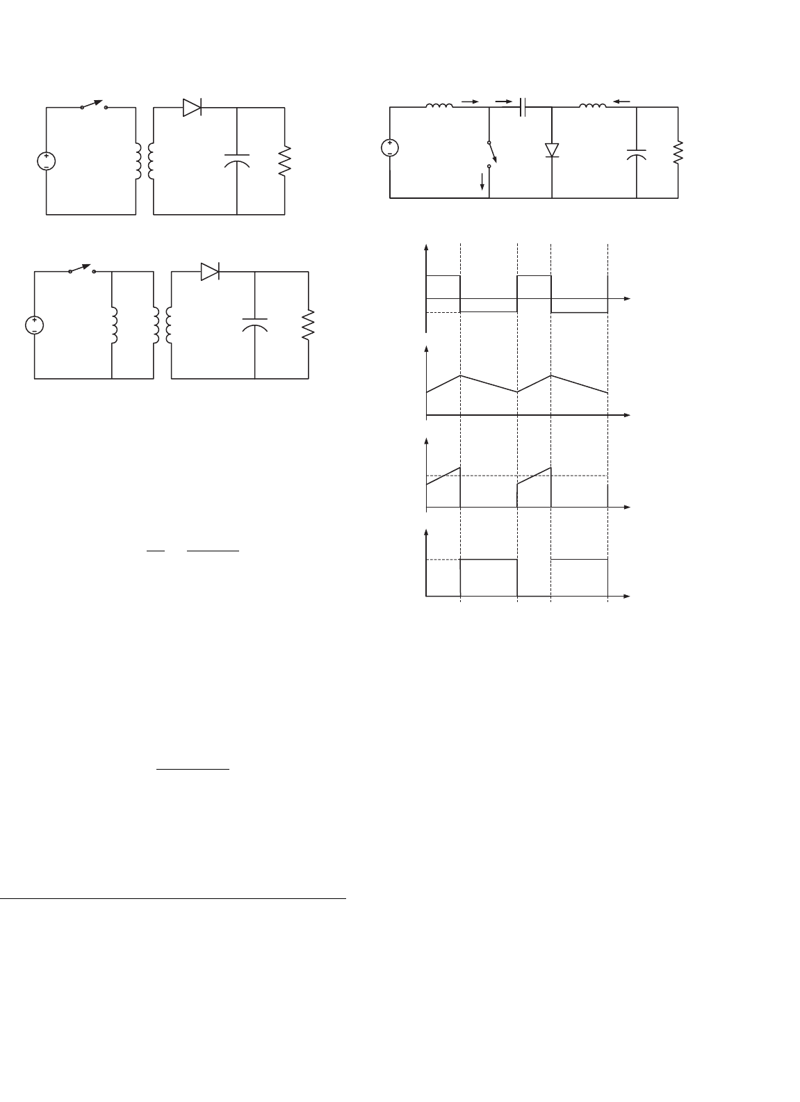
13.9 Control Principles
A dc–dc converter must provide a regulated dc output
voltage under varying load and input voltage conditions.
256 D. Czarkowski
The converter component values are also changing with time,
temperature, pressure, etc. Hence, the control of the output
voltage should be performed in a closed-loop manner using
principles of negative feedback. Two most common closed-
loop control methods for PWM dc–dc converters, namely,
the voltage-mode control and the current-mode control, are
presented schematically in Fig. 13.17.
In the voltage-mode control scheme shown in Fig. 13.17a,
the converter output voltage is sensed and subtracted from
an external reference voltage in an error amplifier. The error
amplifier produces a control voltage that is compared to a
constant-amplitude sawtooth waveform. The comparator pro-
duces a PWM signal which is fed to drivers of controllable
switches in the dc–dc converter. The duty ratio of the PWM
signal depends on the value of the control voltage. The fre-
quency of the PWM signal is the same as the frequency
of the sawtooth waveform. An important advantage of the
voltage-mode control is its simple hardware implementation
and flexibility.
Error
Amplifier
Comparator
And
Latch
dc-dc Converter
dc-dc Converter
Voltage
reference
Voltage
reference
Control
voltage
Control
voltage
Switch or inductor current
Output voltage
Output voltage
Comparator
Sawtooth
waveform
PWM signal
PWM signal
(a)
(b)
Error
Amplifier
FIGURE 13.17 Main control schemes for dc–dc converters: (a) voltage-mode control and (b) current-mode control.
The error amplifier in Fig. 13.17a reacts fast to changes in the
converter output voltage. Thus, the voltage-mode control pro-
vides good load regulation, that is, regulation against variations
in the load. Line regulation (regulation against variations in
the input voltage) is, however, delayed because changes in the
input voltage must first manifest themselves in the converter
output before they can be corrected. To alleviate this problem,
the voltage-mode control scheme is sometimes augmented
by so-called voltage feedforward path. The feedforward path
affects directly the PWM duty ratio according to variations in
the input voltage. As will be explained below, the input volt-
age feedforward is an inherent feature of current-mode control
schemes.
The current-mode control scheme is presented in
Fig. 13.17b. An additional inner control loop feeds back
an inductor current signal. This current signal, converted
into its voltage analog, is compared to the control voltage.
This modification of replacing the sawtooth wavefrom of the
voltage-mode control scheme by a converter current signal