Middleton W.M. (ed.) Reference Data for Engineers: Radio, Electronics, Computer and Communications
Подождите немного. Документ загружается.

42-30
REFERENCE
DATA
FOR ENGINEERS
ADDRESS
200E
2010
2012
2014
2016
2018
201A
201c
201E
2020
2022
SP
-6
‘I
SP
Q
sp-
I
0000
!3
SP
Q
JSR JSR
RTS
JSR RTS RTS
BCNTlS
INSTRUCTION
LFA
STKE,
SP
WCNTlS BCNTlS
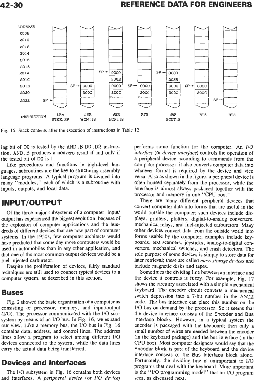
Fig.
15.
Stack contents after the execution
of
instructions in Table
12.
ing bit of
DO
is tested by the
AND.
B
DO,
D2
instruc-
tion.
AND.
B
produces a nonzero result if and only if
the tested bit of
DO
is
1.
Like procedures and functions in high-level lan-
guages, subroutines are the key to structuring assembly
language programs. A typical program is divided into
many “modules,” each of which is a subroutine with
inputs, outputs, and local data.
INPUT/OUTPUT
Of the three major subsystems of a computer, input/
output has experienced the biggest evolution, because of
the explosion of computer applications and the hun-
dreds of different devices that are now part of computer
systems. In the
1950s,
few computer architects would
have predicted that some day more computers would be
used in automobiles than in any other application, and
that one of the most common output devices would be a
fuel-injected carburetor.
Despite the proliferation of devices, fairly standard
techniques are still used to connect typical devices to a
computer system, as described in this section.
Buses
Fig.
2
showed the basic organization
of
a computer
as
consisting of processor, memory, and input/output
(IIO).
The processor communicated with the I/O sub-
system by means of an
110
bus. In Fig.
16,
we expand
our view. Like a memory
bus,
the
I/O
bus in Fig.
16
contains data, address, and control lines. The address
lines allow a program to select among different
I/O
devices connected to the system, while the data lines
carry the actual data being transferred.
Devices and Interfaces
The IIO subsystem in Fig.
16
contains both devices
and interfaces.
A
peripheral device
(or
IIO
device)
performs some function for the computer. An
ZIO
interface
(or
device interface)
controls the operation of
a peripheral device according to commands from the
computer processor, it also converts computer data into
whatever format is required by the device and vice
versa.
Also
as shown in the figure, a peripheral device
is
often housed separately from the processor, while the
interface
is
almost always packaged together with the
processor and memory in one
“CPU
box.”
There are many different peripheral devices that
convert computer data into forms that
are
useful in the
world outside the computer; such devices include dis-
plays, printers, plotters, digital-to-analog converters,
mechanical relays, and fuel-injected carburetors. Many
other devices convert data from the outside world into
forms usable by the computer; examples include key-
boards, text scanners, joysticks, analog-to-digital con-
verters, mechanical switches, and crash detectors. The
sole purpose of some devices is simply to store data for
later retrieval; these are called
mass
storage devices
and
include magnetic disks and tapes.
Sometimes the dividing line between an interface and
the device it controls is fuzzy. For example, Fig. 17
shows the circuitry associated with a simple mechanical
keyboard. The encoder circuit converts a mechanical
switch depression into a 7-bit number in the
ASCII
code. The bus interface can place
this
number on the
I/O
bus on demand by the processor.
So
it
seems that
the device interface consists of the
Encoder
and
Bus
Interface
blocks. However, in a typical system the
encoder is packaged with the keyboard; then only a
small number of wires are needed between the encoder
(in the keyboard package) and the bus interface (in the
CPU
box). Most computer designers would say that the
Encoder
block
is
part
of
the keyboard and the device
interface consists
of
the
Bus
Interface
block alone.
Fortunately, the dividing line is unimportant to
I/O
programs that deal with the keyboard. More important
is the “I/O programming model” that an I/O program
sees, as discussed next.
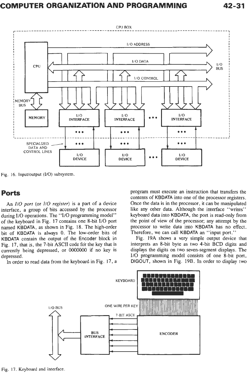
COMPUTER ORGANIZATION AND PROGRAMMING
42-31
DATA AND
CONTROL LINES
Fig.
16.
InpuUoutput (YO) subsystem.
Ports
An
I10
port
(or
I/O
register)
is a part of a device
interface, a group of bits accessed by the processor
during I/O operations. The “I/O programming model”
of the keyboard in Fig. 17 contains one 8-bit
I/O
port
named
KBDATA,
as shown in Fig.
18.
The high-order
bit of
KBDATA
is always
0.
The low-order bits of
KBDATA
contain the output of the
Encoder
block in
Fig.
17,
that is, the 7-bit ASCII code for the key that is
currently being depressed, or
0000000
if no key is
depressed.
In order to read data from the keyboard in Fig.
17,
a
program must execute
an
instruction that transfers the
contents
of
KBDATA
into one of the processor registers.
Once the data is in the processor, it can be manipulated
like any other data. Although the interface “writes”
keyboard data into
KBDATA,
the port is read-only from
the point
of
view
of
the processor;
any
attempt by the
processor
to
write data into
KBDATA
has no effect.
Therefore, we can call
KBDATA
an
“input port.”
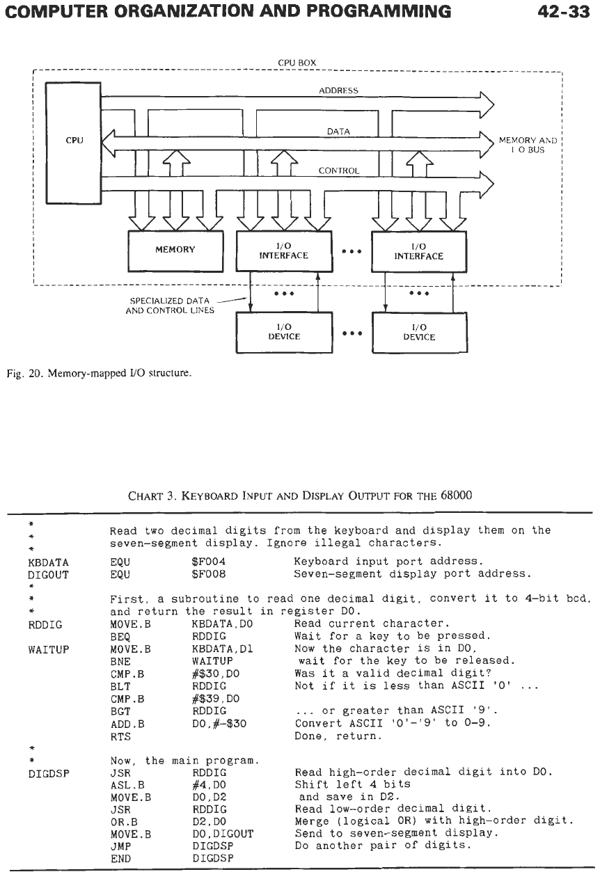
Fig. 19A shows a very simple output device that
interprets
an
8-bit byte as two 4-bit
BCD
digits and
displays the digits on two seven-segment displays. The
I/O
programming model consists
of
one 8-bit port,
DIGOUT,
shown in Fig. 19B. In order to display two
ONE
WIRE PER KE
I/O
BUS
~
7-BIT ASCII
P
-
ENCODER
4
d
Fig.
17.
Keyboard
and
interface.
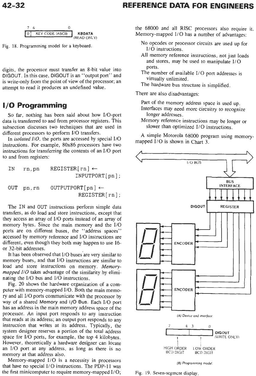
42-32
76
0
0
I
KEY
CODE IASCII)
KBDATA
(READ
ONLY)
Fig.
18.
Programming model
for
a
keyboard.
digits, the processor must transfer an 8-bit value into
DIGOUT.
In this case,
DIGOUT
is an “output port” and
is write-only from the point of view of the processor; an
attempt to read it produces an undefined value.
I/O
Programming
So
far, nothing has been said about how I/O-port
data is transferred to and from processor registers. This
subsection discusses two techniques that are used in
different processors to perform
I/O
transfers.
In
isolated
IIO,
the ports are accessed by special
I/O
instructions. For example, 80x86 processors have two
instructions for transferring the contents of an I/O port
to and from registers:
IN
rn,pn REGISTER[rn]+-
INPUTPORT[pn];
OUT
pn,rn OUTPUTPORT[pn]
+-
REGISTER[rn];
The
IN
and
OUT
instructions perform simple data
transfers, as do load and store instructions, except that
they access an array of
I/O
ports instead of an array of
memory bytes. Since the main memory and the 110
ports are on different buses, the “address spaces”
accessed by memory reference and I/O instructions are
different, even though they both may happen to use 16-
or 32-bit addresses.
It has been observed that I/O buses‘are very similar to
memory buses, and that I/O instructions are similar to
load and store instructions on memory.
Memory-
mapped
I/O
takes advantage of the similarity by elimi-
nating the
I/O
bus and
I/O
instructions.
Fig.
20
shows the hardware organization of a com-
puter with memory-mapped
I/O.
Both the main memo-
ry
and all
I/O
ports communicate with the processor by
way of
a
shared
Memory
and
1/0
Bus.
Each
I/O
port
has an address in the main memory address space of the
processor. An input port responds to any instruction
that reads at its address; an output port responds to any
instruction that writes at its address. Typically, the
system designer reserves a portion of the total address
space for
I/O
ports, for example, the top
4
kilobytes.
However, theoretically a hardware designer can locate
an I/O port at any address, as long as there is no
memory at that address
also.
Memory-mapped 110 is a necessity in processors
that have no special I/O instructions. The PDP-11 was
the first minicomputer to require memory-mapped
I/O;
the 68000 and all RISC processors
also
require it.
Memory-mapped 110 has a number of advantages:
No
opcodes or processor circuits are used up for
I/O instructions.
All memory reference instructions, not
just
loads
and stores, may be used to manipulate I/O
ports.
The number of available
I/O
port addresses is
virtually unlimited.
The hardware bus structure is simplified.
There are also disadvantages:
Part of the memory address space is used up.
Interfaces may need more circuitry to recognize
Memory reference instructions may be longer or
A simple Motorola 68000 program using memory-
longer addresses.
slower than optimized
IiO
instructions.
mapped
I/O
is
shown in Chart 3.
I?
1/0
BUS
DIGOUT
I
REGISTER
(A)
Deuice
ond
interface
7
43
I
I
HIGH ORDER
LOW
ORDER
BCD
DIGIT
BCD DIGIT
(E)
Programming model
Fig.
19.
Seven-segment display.
COMPUTER ORGANIZATION AND PROGRAMMING
42-33
MEMORY
AND
Fig.
20.
Memory-mapped
IiO
structure.
CHART
3.
KEYBOARD
INPUT AND
DISPLAY
OUTPUT
FOR
THE
68000
*
*
*
Read two decimal digits from the keyboard and display them on the
seven-segment display. Ignore illegal characters.
KBDATA EQU $F004 Keyboard input port address.
DIGOUT EQU $F008 Seven-segment display port address.
*
*
First, a subroutine
to
read one decimal digit, convert it to 4-bit bcd,
*
and return the result in register DO.
RDDIG
MOVE. B
KBDATA, DO Read current character.
WAITUP
MOVE
.B
KBDATA,Dl Now the character is in DO,
BE4 RDDIG Wait
for
a key to be pressed.
BNE WAITUP wait
for
the key to be released.
CMP
.
B
#$SO,
DO Was it a valid decimal digit?
BLT RDDIG Not if it is less than ASCII
'0'
...
CMP
.
B
BGT RDDIG
...
or
greater than ASCII
'9'.
ADD.
B
DO,
#-$30
Convert ASCII
'0'-'9'
to
0-9.
RTS
Done, return.
#$39
I
DO
*
*
Now, the main program.
DIGDSP
J
SR RDDIG Read high-order decimal digit into DO.
Shift left
4
bits
ASL
.
B
#4,
DO
MOVE. B DO, D2 and save in D2.
JSR RDDIG Read low-order decimal digit.
0R.B D2, DO Merge (logical OR) with high-order digit.
MOVE. B DO, DIGOUT Send to seven-segment display.
JMP DIGDSP Do another pair
of
digits.
END DIGDSP
43
Logic Design
Edward
J.
McCluskey
Introduction
43-2
Postulates
43-2
Analysis
43-3
Synthesis
43-4
Canonical Expressions
Networks
Theorems
43-8
Single-Variable Theorems
Two- and Three-Variable Theorems
Example
n-Variable Theorems
General Gate Networks
43-10
The Map Method
43-12
Maps for Two, Three, and Four Variables
Prime Implicants
Formation
of
Minimal
Sums
Sequential Circuits
43-16
43-
1
43-2
INTRODUCTION
The distinguishing feature of the circuits to be
discussed in this chapter is the use of two-valued, or
binary, signals. There will be some deviation of the
signals from their nominal values, but within certain
limits this variation will not affect the performance of
the circuit. If the variations exceed these limits, the
circuit will not behave properly, and steps must be taken
to
confine the signals to the proper ranges. When the
statement is made that the signals are two-valued, what
is really meant is that the value of each signal is within
one of two (nonoverlapping) continuous ranges. Since
the operation of the circuit does not depend on exactly
which value within a given range the signal takes on, a
particular value is chosen to represent the range, and the
signal is said to be equal to this value. The exact
numerical value of the signal is not important. It
is
possible to have two circuits perform the same function
and have completely different values for their signals. In
order to avoid any possible confusion that might arise
because of this situation and to simplify the design
procedures, it is customary to carry out the logic design
without specifying the actual values of the signals. Once
the logic design has been completed, the actual values
must be assigned to the signals in the course
of
designing the detailed electrical circuit. For the purpos-
es
of
the logic design, arbitrary symbols are chosen to
represent the two values to which the signals are to be
restricted. An algebra* using these symbols
is
then
developed as the basis for formal design techniques.
The development of such an algebra will be described
next.
POSTULATES
The two symbols most commonly chosen to represent
the two logic values taken on by binary signals are
0
and
1.
It should be emphasized that these logic symbols
have no numerical significance. For an electronic circuit
that has its signals equal to either
0
or
5
volts, logical
1
usually represents
5
volts and logical
0
represents
0
volts. This choice-in which
1
corresponds to the more
positive physical value-is called
positive logic. Nega-
tive
logic
uses logic
1
for the more negative physical
value; it is much less common than positive logic, but is
natural when the active signal value corresponds to the
lower physical value (as in PMOS, for example). We
will use positive logic here.
Other symbols such as T and F,
H
and
L,
or
+
and
-
are also used. Logicians like
T
and
F.
IC
data books
favor
H
and
L.
Switching variables are used in logic networks to
represent the signals present at gate inputs and outputs.
lK
-T-
Fig.
1.
The transmission,
T,
of
a switch.
Switching variables can also represent the state of a
switch. Fig.
1
shows this. The switch operation is
defined as the two switch terminals
(a
and
b)
being
connected together
if
and only if the
control variable,
K,
equals 1. When
K
=
0,
there is an open circuit
between the two switch terminals. There is a variable,
T,
associated with the switch that equals
1
when the
terminals are connected together and that equals
0
when
there is an open circuit between the terminals. The
variable,
T,
is called the
transmission
of the switch. (It
is also possible to associate with the switch a variable
that equals
1
only when the switch is open. Such a
variable is called the
switch hindrance.
This was used in
the very early papers on switching theory in connection
with contact networks. The transmission concept
is
the
standard usage at present.)
The first postulate of the switching algebra can now
be presented. This is merely a formal statement of the
fact that switching variables are always equal to either
0
or
1.
(In the statements of postulates and theorems that
follow, the symbols X,
Y,
Z,
XI, X,
. . .
,
X, will be
used to represent switching variables.)
(pl)X=OifX#
1
(P1’)X= 1ifxZO
To implement general switching networks, it is neces-
sary
to be able to obtain, for any signal representing a
switching variable, a signal that has the opposite value.
A
circuit for realizing this function is called an
inverter.
Fig.
2
shows two of the most common inverter symbols.
If
X
represents a switching variable, the symbol X’ is
used to represent the signal having the opposite value.
This notation is specified formally in the second switch-
ing-algebra postulate:
(P2)
(P2‘)
If X
=
0,
then X’
=
1
ifX
=
1,
thenX’
=
0
*This algebra will be called
switching
algebra. It is
x
X‘
identical with a Boolean algebra and was originally applied to
x+
X’
switching circuits (reference
1)
by reinterpreting Soolean
algebra in terms of switching circuits rather than by develop-
ing
a
switching algebra directly, as will be done here.
Fig.
2.
Inverter symbols.
LOGIC DESIGN
43-3
The two symbols,
X
and
X‘,
are
not
two different
variables, since they involve only
X.
In
order to
distinguish them, the term
literal
is used, where a literal
is defined as a variable with or without an associated
prime, and
X
and
X’
are different literals. The literal
X’
is called the
complement*
of
X.
Similarly,
0
is called
the complement of 1, and
1
is called the complement of
0.
The logical operation of the inverter can now be
described in terms of switching algebra. If
Xl
represents
the input signal and
X,
the output signal, then
Xo
=
XI’,
since
X,
is high when
XI
is low, and vice versa.
Multiple-input gates require additional algebraic op-
erations. A two-input
AND
gate will be considered first.
If
XI
and
X2
represent its
two
inputs and
Xo
its output,
Fig.
3A
shows its logical performance. This table is also
correct for the transmission,
X,,
of two switches,
XI
and
X,
,
in series. The operation represented
is
identical
with ordinary multiplication and will be defined
as
multiplication in the switching algebra developed here.
Thus, the’equation for an
AND
gate, or two switches in
series, is
Xo
=
XlX2.
The table for an
OR
gate, or two switches in parallel,
is shown in Fig. 4A. This table will be taken as the
definition of switching-algebra addition.? It is identical
with ordinary addition except for the case
1
+
1
=
1.
The remaining postulates are merely restatements of the
definitions of multiplication and addition:
(P3)
0
’
0
=
0
(P3’)
1
+
1
=
1
(P4)
1.
1
=
1
(P4’)
0
+
0
=
0
(P5)
1*0=0.1=0
(P5’)
O+l=
1+0=1
*Some authors use the symbols
x
or
-X
to indicate the
tThis operation is also called logical addition, and some
complement of
X.
writers use the notation
x,
v
x2
rather than
x1
+
x2.
x1
x,
0
1
Om
(C)
Serles
switches.
Fig.
3.
The
AND
function.
(B)
Symbols.
x1
X2
1
XO
x,=x,+x,
a{+$-b
-x,-
(Aj
Table.
(Cj
Parallel switches
xo
(Bj
Symbols.
Fig.
4.
The
OR
function.
All the postulates have been stated in pairs. These
pairs have the property that when
(0
and
1)
and
(+
and
.)
are interchanged, one member of the pair
is
changed into the other. This is an example of the
general
principle
of
duality,
which is true for all
switching-algebra theorems since it is true for all the
postulates. This algebraic duality arises from the fact
that either
1
or
0
can be assigned to the high voltage or
to an open circuit. If
0
is chosen to represent a high
voltage, the expression for an
AND
gate becomes
xo
=
x1
+
x2.
Similarly, the transmission of two switches in
series is equal to
xl
+
x2
if
0
is chosen to represent a
closed circuit.
ANALYSIS
Analysis of a circuit consists in examining the circuit
and somehow determining what the behavior of the
circuit will be for all possible inputs. The switching
algebra developed in the previous section is sufficient
for the analysis of those switching circuits that are
known as
combinational switching circuits.
A combina-
tional switching circuit is defined as one for which the
outputs depend only
on
the present inputs to the circuit.
The other type of circuit, called a
sequential switching
circuit,
is one for which the outputs depend not only on
the present inputs but
also
on the
past history
of
the
inputs. Acyclic networks (networks with no feedback
loops) of gates
are
always combinational. Sequential
circuits typically contain latches, flip-flops, or feedback
Combinational circuits are analyzed by writing an
algebraic function for each output. These are functions
of the input variables from which the condition of each
output can be determined for each combination of input
conditions. For a switch network, these output func-
tions are the transmissions between each pair
of
external
loops.
43-4
REFERENCE
DATA
FOR ENGINEERS
terminals. Only two-terminal networks will be consid-
ered for the present. In a gate network, an output
function specifies those input conditions for which the
voltage of an output node will be at the high level.
Fig.
5
shows a very simple analysis example. In an
acyclic network, there will be at least one gate, such as
the
OR
gate in Fig.
5,
that has only network inputs
connected to it. The output of such gates can be written
down directly. There will then be other gates that have
either input variables or expressions on all their inputs;
the
AND
gate
in
Fig.
5
is such a gate. It is then possible
to write expressions for the output of all these gates. By
repeating this procedure, an expression will eventually
be obtained for the network output.
A
procedure for using these output functions to
determine the circuit performance is to substitute a set
of values for the input variables and then use the
postulates to simplify the resulting expressions.
A
value
for the output function will be obtained that specifies
the output for the particular input combination chosen.
For example, if the input combination
XI
=
1,
X2
=
1,
X3
=
0,
X4
=
1,
is chosen, the output function of Fig.
5
becomes
=
1
*
l(0
+
1)
=
l(1)
=
I
By carrying out this procedure for all possible input
combinations, it is possible to form a table that lists the
output for each input combination. Such a table de-
scribes completely the circuit performance and is called
a
table
of
combinations.*
Table
I
is the table of
combinations for the circuit of Fig.
5.
SYNTHESIS
To design a combinational circuit, the procedure just
described must be reversed. The designer writes a table
of combinations that specifies the desired circuit per-
formance. From this table, an algebraic function is
written from which a circuit can be derived.
A
concise
means of specifying the table of combinations, called a
decimal speci$cation,
is to list the numbers of the rows
for which the output is to equal
1.
For Table
1,
this
specification
is:
f(X,, X2, X3, X,)
=
C(13,
14,
1.5)
*In
logic,
the
table
is
called
a
truth
ruble,
and some
writers
use
this
term
when
discussing switching
circuits.
XI
x2
w3
+
x4,
Fig.
5.
Simple example
of
analysis
of a
gate network.
TABLE
1.
TABLE
OF
COMBINATIONS
FOR
0
1
2
3
4
5
6
7
8
9
10
11
12
13
14
15
XI
x2
x3
x4
0 0
0
0
0
0
0
1
0 0
1
0
0 0
1
1
0
1
0
0
0
1
0
1
0
1
1
0
0
1
1
1
1
0
0
0
1
0
0
1
1
0
1
0
1
0
1
1
I
1
0
0
1
1
0
1
1
1
1
0
1
1
1
1
-
f
0
0
0
0
0
0
0
0
0
0
0
0
0
1
1
1
where the
2
signifies that the rows for which the
function equals 1 are being listed. It is also possible
to
list the rows for which the function equals
0,
such a list
being preceded by the symbol
II
to indicate that it is the
zero rows which are listed. This specification for the
preceding table is
f(xr,
x2>
x3>
x4)
=
II(0,
1,
2,
3,
4,
5,
6,
7,
8,
9,
10,
11,
12).
In order
to
avoid any ambiguity in these specifica-
tions, it is necessary to adopt some rule for numbering
the rows of the table of combinations. The usual
procedure is to regard each row
of
the table as a binary
number and then use the decimal equivalent of this
binary number as the row number. The output-column
entries are not included in forming the binary row
numbers. There is nothing special about decimal num-
bers other than the fact that they are the most familiar;
any other number base, such as octal, could be used.
The reason for using a number system other than binary
is simply that binary numbers take
too
much space to
write down.
It has been pointed out that the table of combinations
is a complete specification for a combinational circuit.
The first step in designing
a
circuit is to formulate such a
table. There are no general formal techniques for doing
this. When a sequential circuit is being designed, it is
customary to reduce the sequential-design problem to
(several) combinational problems, and formal tech-
niques exist for doing this. However, when
a
combina-
tional circuit is being designed,
no
formal techniques
are available, and it is necessary
to
rely on common
sense. This is not too surprising, since any formal
technique must start with a formal statement of the
problem, and this
is
precisely what the table of combi-
nations is.
As
an example of how this is done, the table
of combinations for a circuit
to
check binary-coded
decimal digits for the
8,
4,
2,
1
code is shown in Table
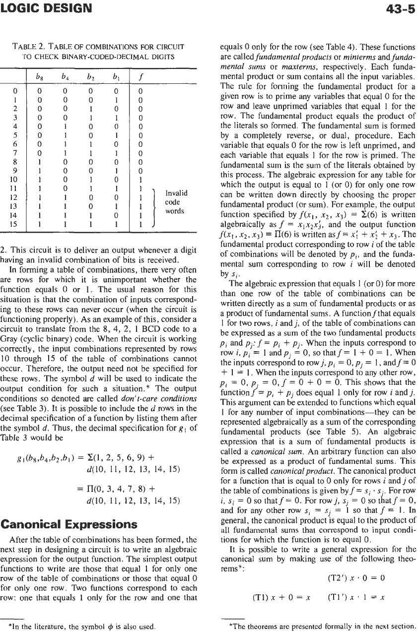
TABLE 2. TABLE
OF
COMBINATIONS
FOR
CIRCUIT
TO
CHECK BINARY-CODED-DECIMAL
DIGITS
-
-
0
1
2
3
4
5
6
7
8
9
10
11
12
13
14
15
-
b8
b4
b2
bl
0000
0001
0010
0011
0100
0101
0110
0111
1000
1001
1010
101
1
1100
1101
1
1 10
1
1 1 1
f
0
0
0
0
0
0
0
0
0
0
1
words
1
2. This circuit is to deliver an output whenever a digit
having an invalid combination of bits is received.
In forming a table of combinations, there very often
are rows for which it is unimportant whether the
function equals
0
or
1.
The usual reason for this
situation
is
that the combination of inputs correspond-
ing to these rows can never occur (when the circuit is
functioning properly).
As
an example of this, consider a
circuit to translate from the
8,
4,
2, 1
BCD
code to a
Gray (cyclic binary) code. When the circuit is working
correctly, the input combinations represented by rows
10 through 15 of the table of combinations cannot
occur. Therefore, the output need not be specified for
these rows. The symbol
d
will be used to indicate the
output condition for such a situation.* The output
conditions
so
denoted are called
don’ t-care conditions
(see Table 3). It is possible to include the
d
rows in the
decimal specification of a function by listing them after
the symbol
d.
Thus, the decimal specification for
gl
of
Table 3 would be
gi(b8h4,hbl)
=
XU, 2,
5,
6,
9)
+
=
n(0,
3,
4,
7,
8)
+
d(10,
11, 12, 13, 14, 15)
d(10,
11, 12, 13,
14,
15)
Canonical Expressions
After the table of combinations has been formed, the
next step in designing a circuit is to write an algebraic
expression for the output function. The simplest output
functions to write are those that equal
1
for only one
row of the table of combinations or those that equal
0
for only one row. Two functions correspond to each
row: one that equals 1 only for the row and one that
*In
the
literature,
the
symbol
q5
is
also
used.
equals
0
only for the row (see Table
4).
These functions
are called
fundamental products
or
minterms
and
finda-
mental
sums
or
maxterms,
respectively. Each funda-
mental product or sum contains all the input variables.
The rule for forming the fundamental product for a
given row is to prime any variables that equal
0
for the
row and leave unprimed variables that equal 1 for the
row. The fundamental product equals the product of
the literals
so
formed. The fundamental sum is formed
by a completely reverse, or dual, procedure. Each
variable that equals
0
for the row is left unprimed, and
each variable that equals 1 for the row is primed. The
fundamental sum is the sum of the literals obtained by
this process. The algebraic expression for any table for
which the output is equal
to
1 (or
0)
for only one row
can be written down directly by choosing the proper
fundamental product (or sum). For example, the output
function specified by
f(xl,
x2,
x3)
=
8(6)
is written
algebraically as
f
=
xIx2x;,
and the output function
f(xl,
x2, x3)
=
n(6)
is written asf=
xi
+
xi
+
x3.
The
fundamental product corresponding to row
i
of the table
of combinations will be denoted by
pi,
and the funda-
mental sum corresponding to row
i
will be denoted
The algebraic expression that equals
1
(or
0)
for more
than one row of the table of combinations can be
written directly as a sum of fundamental products or as
a product of fundamental sums. A functionfthat equals
1 for two rows,
i
and
j,
of the table of combinations can
be expressed as a sum of the two fundamental products
pi
and
pj:
f
=
pi
+
pj.
When the inputs correspond to
row
i,
pi
=
1
andpj
=
0,
so
thatf
=
1
+
0
=
1.
When
the inputs correspond
to
row
j,
pi
=
0,
pj
=
1,
and
f
=
0
+
1
=
1. When the inputs correspond to any other row,
pi
=
0,
p.
=
0,
f
=
0
+
0
=
0.
This shows that the
function
f
=
pi
+
pj
does equal 1 only for row
i
and
j.
This argument can be extended to functions which equal
1 for any number of input combinations-they can be
represented algebraically as a sum of the corresponding
fundamental products (see Table
5).
An algebraic
expression that is a sum of fundamental products is
called a
canonical sum.
An arbitrary function can also
be expressed as a product of fundamental sums. This
form is called
canonical product.
The canonical product
for a function that is equal to
0
only for rows
i
and
j
of
the table of combinations
is
given by
f
=
si
sj.
For row
i,si
=Osothatf=O.Forrowj,sj=Osothatf=O,
and for any other row
si
=
si
=
1
so
that
f
=
1. In
general, the canonical product is equal to the product of
all fundamental sums that correspond
to
input condi-
tions for which the function is to equal
0.
It is possible to write a general expression for the
canonical sum by making use of the following theo-
rems
*
:
by
si.
I
(T2’)
x
*
0
=
0
(T1’)x. 1
=x
(T1)x
+
0
=
x
*The theorems are presented formally
in
the
next
section.