Martin P.M. Handbook of Deposition Technologies for Films and Coatings, Third Edition: Science, Applications and Technology
Подождите немного. Документ загружается.


CHAPTER 18
Jet Vapor Deposition
Paul Komarenko, Michael Drago, Michael Gorski, Takashi Tamagawa
and Bret Halpern
Jet Process Corporation, 57B Dodge Avenue, North Haven, CT 06473, USA
18.1 Introduction 881
18.2 Principles of JVD Sources and Systems 882
18.3 Relative Motion between Jet Sources and Substrates 885
18.4 Three JVD Jet Sources 890
18.4.1 Wirefeed to Hot Filament Source 890
18.4.2 Hollow Cathode Sputter Jet Source 891
18.4.3 Wick Jet Capillary Feed Source 892
18.5 Generation and Deposition of Atoms and Clusters 893
18.6 Application of JVD to Solder and Related Layers 894
18.7 Summary 897
18.1 Introduction
Jet Vapor Deposition
TM
(JVD
TM
) uses high-speed inert gas jets to carry film components to
substrates. This transport takes place in a fast flow system, mechanically pumped to pressures
in the range of 1 torr. Developed by Jet Process Corporation (JPC) and now used
commercially, JVD has been applied to a wide range of thin and thick film applications,
demonstrating an adaptability to new problems, and a versatility for making complex materials
quickly and economically.
Our work in the past shows that JVD is particularly well suited to solder deposition for
microelectronic packaging, where there is a growing need to solder small electronic devices on
ever smaller circuit features at higher density. Deposition of the required solder bumps, often
of expensive alloys such as eutectic AuSn, taxes the capability of standard techniques to
produce correct properties in an economical way. JVD is thus fast becoming a method of
choice, and JPC has become an important supplier of solder layers and related adhesion,
diffusion barrier, and protective cap layers.
JVD’s signature innovation is a novel vapor source: a sonic jet in low vacuum which transports
condensable atoms, molecules, or clusters, to a substrate and deposits them efficiently in a
Copyright © 2010 Peter M. Martin. Published by Elsevier Inc.
All rights reserved.
881

882 Chapter 18
small area. Larger areas are coated by arranging for relative two-dimensional (2D) motion
between substrate and one or more jet sources. The combination of jet sources and
mechanisms for jet–substrate relative motion characterizes JVD.
The use of the jet in low vacuum for deposition, first investigated by Halpern [1] and later by
Schmitt and Halpern [2, 3], has opened new pathways to both microscopic property control and
manufacturing efficiency. JPC has developed several jet sources based on different principles,
which are now basic components of a multiple jet, moving substrate process [4] for depositing
metals, semiconductors, dielectrics, oxides, nitrides, and organics. These materials can be
grown by JVD in many forms: multicomponent, alloy, multilayer, host–guest, and nanocluster
films. The growth rates are high, approaching in some cases micrometers per minute over areas
of several hundred cm
2
. Deposition is carried out without toxic precursors or effluent, on
substrates that remain cool, near room temperature. By straightforward control of jet source
conditions, JVD can generate and deposit either atoms or nanoclusters, both at high rate.
Atoms and clusters behave differently in deposition, particularly in penetration of photoresist
mask windows needed for solder bump deposition. All these features of JVD are valuable for
deposition of solder and related layers. JVD is deceptively simple, but it has a fortunate
combination of useful characteristics, which will be discussed in the following sections:
Section 18.2: Principles of JVD sources and systems
Section 18.3: Relative motion between jet source and substrates
Section 18.4: Three JVD jet sources
Section 18.5: Generation and deposition of atoms and clusters
Section 18.6: Application of JVD to solder and related layers.
Apart from solder deposition, the previous edition of this Handbook described a variety of past
applications showing the range of JVD. These applications and related references are briefly
summarized in the Appendix.
18.2 Principles of JVD Sources and Systems
Jet sources can have different designs, but all are mounted on flanges aimed into a
low-pressure deposition chamber. A fast flow of inert gas through each jet source is sustained
by a mechanical pump and Roots blower [5, 6] with pumping speeds typically in the range of
5000–10,000 liters/minute, but sometimes higher or lower. These pumps comprise a reliable,
inexpensive vacuum technology.
A typical jet source is a 3 inch (7.62 cm) diameter cylindrical nozzle, with an endplate having
an exit orifice ∼ 1 cm in diameter. Helium or argon, and occasionally nitrogen, is supplied to
the nozzle and exits from it as a jet. Ordinarily the nozzle pressure P
n
is several torr, and the
Jet Vapor Deposition 883
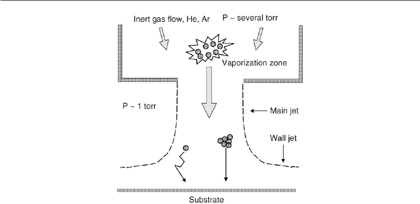
Figure 18.1: Generalized jet source, showing nozzle, main jet, and wall jet. The nozzle exit
diameter is typically 1 cm. Metal atoms are vaporized near exit, deposit in localized area.
Trajectories before impact: atom, diffusive; cluster, straight.
downstream pressure P
d
is 1 torr or less, but the range may be wide: in different applications
both pressures can be higher or lower. When the ratio P
n
/P
d
> 2, the flow is critical, and the jet
emerges at the speed of sound; for He at 298 K, the exit velocity is ∼ 10
5
cm/s. There is
considerable latitude in the source shape, orifice size, and operating parameters of a jet source.
Figure 18.1 shows a generalized jet source.
The jet can entrain any atomic, molecular, or cluster vapor, and convey it to a substrate for
condensation. A vapor source is placed upstream of the nozzle exit, a region in which the
carrier gas is accelerating toward the speed of sound. Depending on the material, vaporization
can be effected by several techniques, such as thermal evaporation, glow discharge sputtering,
and microwave plasma or direct current (DC) discharge reaction. Atoms of gold, for example,
injected upstream into the He flow will be swiftly captured and transported downstream by the
jet. On a flat substrate placed perpendicular to the jet, and several centimeters downstream, a
bright gold deposit will quickly appear; virtually all the gold atoms deposit in a circular zone
comparable to the nozzle exit area. The deposit is symmetric but non-uniform, being thicker
toward the center. The capture efficiency for metal atoms is generally high, and for clusters
even higher; Figure 18.1 indicates the trajectories of an atom and a cluster before impact on
the substrate. We will discuss later the designs of three sources based on different vapor
generation approaches.
The use of single or multiple jets in JVD synthesis follows from the structure of a single inert
gas jet. The jet contour can be made visible by atomic emission from a plasma ignited in the

884 Chapter 18
jet, or by chemiluminescence, say from active N
2
. The structure of free jets issuing from
small-diameter nozzles at high pressure has been amply described [7], but particularly useful
features arise under JVD conditions, where the nozzle exit diameters are relatively large,
∼ 1 cm, and the nozzle pressures are usually between 1 and 10 torr.
On exiting the nozzle, the jet expands into a zone of reduced density in which nearly all atoms
move in the same direction at the speed of sound. In JVD this zone is nearly collision free; it
terminates at the Mach disk, located a distance x ∼ 0.67 d
n
(P
n
/P
d
)
1/2
downstream of the nozzle
of diameter d
n
[7]. The pressure ratio usually lies in the range 2 < P
n
/P
d
< 10, and the Mach
disk is located several nozzle diameters, or several centimeters, downstream. Beyond the Mach
disk the density rises sharply to the downstream background value, the jet speed drops to
∼ 3 × 10
4
cm/s, determined by the system pumping speed, and collisions again occur in the jet.
Further downstream the jet diverges little, under typical JVD conditions, and remains fairly
collimated over distances of tens of centimeters.
Jet collimation has important consequences. Because axial transport is much faster than radial
diffusion, the jet remains a spatially distinct source independent of other nearby jets, so that
several jets can be operated close to each other.
A heavy atom injected into the light carrier jet will travel with the jet, but will also execute a
‘random walk’. For example, an atom of Au injected on the jet axis will diffuse a distance x
away from the axis during the transit time to the substrate τ = L/v according to
x
2
∼ 2 Dτ ∼ 2DL/v (18.1)
where D is the diffusion coefficient, L is the distance to the substrate, and v is the jet speed
downstream of the Mach disk. For L ∼ 10 cm, v ∼ 3×10
4
cm/s, and D ∼ 600 cm
2
/s (diffusion
in He at 1 torr), the diffusion distance is ∼ 4 mm. Therefore most Au atoms will have diffused
only a few millimeters from the axis by the time they arrive at the substrate; they are
effectively trapped within the jet, and cannot easily escape. This already suggests a high
capture efficiency on the substrate, which is particularly important for expensive metals. In a
real jet source, vaporization does not occur exactly on axis, but from an extended area such as
a hot W coil, so that a fraction of Au atoms are nearer the jet boundary and can escape more
readily. But the fraction lost turns out to be small.
On impact with the substrate the free jet flares radially into a wall jet. Visualization
experiments show that the transition from free jet to wall jet is sharp; the thickness of the wall
jet is only a few millimeters. When the Au atoms arrive near the substrate, the wall jet can be
expected to carry some of them away, as well as broaden the deposit. But a thin wall jet favors
deposition; metal atoms in the wall jet can still diffuse fast to the substrate. In the wall jet too,
only a small fraction of gold atoms are transported far enough to be lost.

Jet Vapor Deposition 885
We confirmed the high capture efficiency of Au atoms by mass balance experiments; a known
length of Au wire is vaporized in the nozzle, and the weight deposited downstream is
measured with a microbalance. We found that 95% of the Au wire vaporized in the nozzle
deposited on the substrate, with the remainder carried away in the wall jet. Jet collimation and
localized deposition can be regarded as the JVD equivalent of line of sight deposition in high
vacuum. The deposition efficiency is far higher in JVD, however: all vaporized material goes
in one direction, is confined to the jet, and most of it deposits in the impact zone.
The large inertia of Au atoms entrained in the jet may also favor high capture efficiency. When
the axial He jet transforms sharply into a radial wall jet, heavy Au atoms turn the corner only
with difficulty, and tend to move straight toward the substrate [8]. We have not yet determined
the relative importance of diffusion and inertia in the wall jet region under our operating
conditions, but studies of deposition under conditions of much higher pressure ratio P
n
/P
d
and
much smaller nozzle diameter than JVD do show inertial effects under restricted conditions
[9]. In JVD cluster deposition, inertia plays an important role, to be discussed later.
Simultaneously flowing jets are not only spatially distinct, but the operation of one does not
alter the upstream nozzle conditions of any other. As long as P
n
/P
d
exceeds ∼ 2, the pressure
P
n
in the nozzle remains constant despite changes in downstream P
d
resulting either from
changes in pumping speed or from injection of gas downstream. If the pump can sustain
critical flow, the jets all emerge at the speed of sound, and neither information nor mass can
propagate upstream. Therefore the calibration of one jet source is unaffected by simultaneous
operation of other jets. This makes it possible to run several jet sources together to make
multicomponent films of accurate composition.
Another example of the benefits: we vaporize many metals in a hollow cathode sputter jet, or a
wirefeed jet, and then oxidize the growing metal film with O
2
or O atoms injected
downstream. Inside the nozzle, the metal sputtering target or any other metal vapor source is
then shielded from the oxidants downstream by sonic flow out of the nozzle; a comparable
protection in high-vacuum PVD is nearly impossible.
In sum, JVD’s jets in low vacuum have a relatively simple behavior, despite variations in
density and speed near the Mach disk. The main jet is fast, collimated, and well defined, and
the wall jet is thin. Consequently, the jet delivers metal or other vapor efficiently; deposition is
localized, film growth is fast, and radial wall jet flow does not greatly broaden the deposit.
Multiple jets are basically independent.
18.3 Relative Motion between Jet Sources and Substrates
In order to deposit uniform films over larger areas, the jet source and substrate are moved
relative to each other in two dimensions [4]. Solder must be deposited on a range of substrates
886 Chapter 18
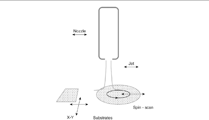
Figure 18.2: Schemes for 2D relative motion between substrate and jet sources. Different
combinations of rotation and translation are possible.
including flat patterned silicon wafers of 2, 4, 6, and 8 inch diameter, rectangular substrates of
similar area, and small components such as CuW heat sinks of irregular shape and millimeter
dimensions. JVD systems must be versatile enough to coat single wafers or batches, by
providing the 2D relative motion between jet and substrate. As shown in Figure 18.2, one can
move the source or the substrate (or even the gas jet itself) with motion control electronics
giving appropriate combinations of rotation and translation. Motion is transmitted
mechanically through chamber walls via bellows assemblies and ferrofluidic seals, or by
stepper motors within the chamber. Figure 18.2 also suggests the various combinations that
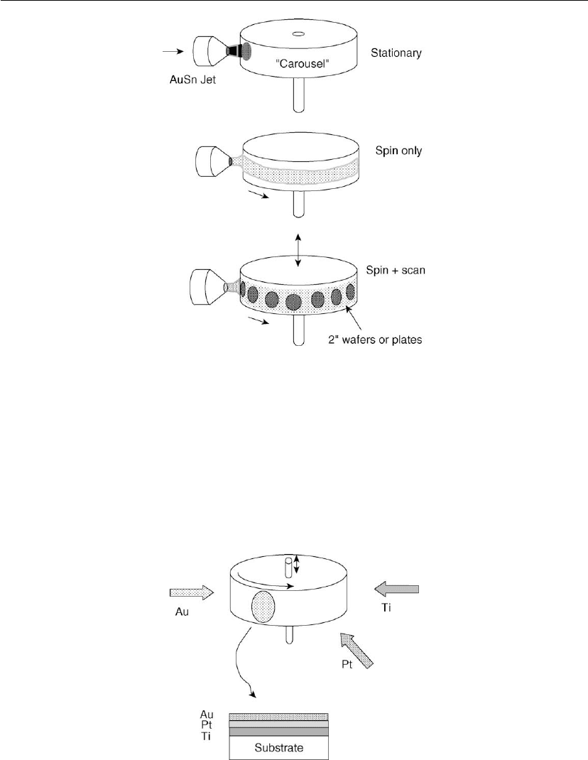
have been implemented at JPC. For example, in Figure 18.3 substrates are mounted on a
carousel which can both spin rapidly and translate slowly along its axis; the carousel motion is
computer controlled, and various motions can be programmed. The jet is aimed radially at
the carousel. If the carousel is only spinning, a band of deposition appears around it; if the
carousel is also vertically scanned at constant speed, the band broadens to cover the entire
carousel surface, and that of any substrate on it. The deposit thickness is uniform because all
areas are exposed for equal times to a constant jet flux. This approach is ideal for batches of
small or moderate sized substrates, where the flatness of the substrate does not depart much
from the curvature of the carousel, so film thickness remains uniform. To keep the size of
carousels and chambers manageable, this batch processing is limited to 4 inch diameter wafers
or 4 × 4 inch squares.
Jet Vapor Deposition 887
Figure 18.3: A spinning, oscillating carousel for batch deposition of uniform films on small wafers
or small substrates of other shape.
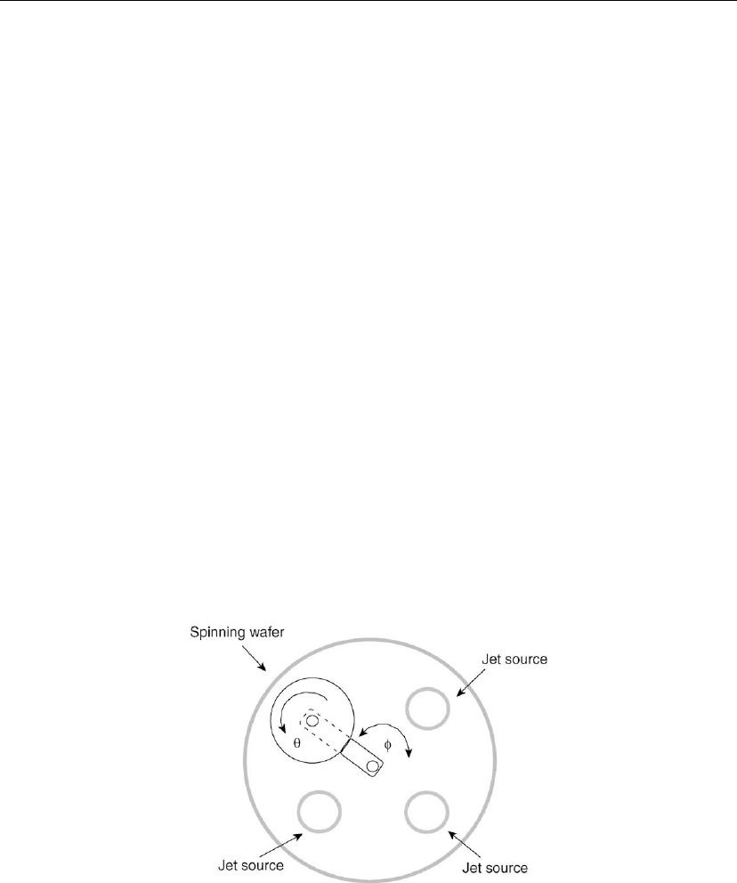
Several jet sources can be aimed at the carousel. To make a layered compound, the jet sources
are run in sequence, as in Figure 18.4, for different times determined by the required layer
thickness. To deposit a multicomponent compound, several jets are run at the same time, while
the substrate is sweeping through all the jets at high speed. Relative motion between substrate
Figure 18.4: Sequential deposition of layers such as Ti, Pt, and Au, using multiple jet, moving
substrate approach for substrates on a carousel.
888 Chapter 18
and several jet sources can often be made so fast that micromixing occurs at submonolayer
level. For example, lead zirconate titanate (PZT) can be made using three metal jets of Pb, Zr,
and Ti, plus a plasma jet of oxygen, by choosing the carousel spin frequency so that less than
one monolayer of any metal is deposited on any substrate during its time of passage through
any of the jets. The three components are then well mixed and quickly converted to oxide by
the oxygen plasma jet.
Larger substrates, such as 4, 6, or 8 inch wafers, or a limited number of small substrates, are
better processed with a single wafer, spin–scan approach, as in the right side of Figure 18.2.
The wafer is mounted on a fast spinning platter; the spin provides one degree of motion, and
slow translation of the jet source or the platter provides the second degree. For example,
the jet source can be mounted on a sliding vacuum flange, while the wafer spins around a
fixed axis; the sliding jet source can then scan the wafer periodically across a diameter. The
scan speed is slow at the wafer’s edge and rapid through the wafer’s center, to equalize
residence times. The correct relation between scan speed and position must be found by
experiment, but this approach gives uniform films and economical use of material for single
wafer coating.
To coat a single wafer with a sequence of metal layers, we move the entire spinning platter
past a sequence of jet sources. The simplest arrangement of sources is either a straight line or a
circle. The spinning wafer visits each jet source in sequence, performing a slow scan back and
forth in front of each source to give the desired multilayer sequence. For example, Figure 18.5
shows a compact index arm configuration in which several sources are arranged in a circle.
Figure 18.5: Index arm deposition system for depositing a sequence of layers on a single wafer.
The wafer spins rapidly through an angle θ, while the index arm moves through angle φ, visiting
each jet source in turn and executing a programmed periodic scan through an arc of angle φ in
front of each source.

Jet Vapor Deposition 889
The index arm first positions one edge of the spinning wafer in front of the first source; the arm
then executes a scan by sweeping the wafer back and forth through a short arc from one edge
of the wafer through the opposite edge. The index arm then indexes to the next jet source,
where the spin and scan motion is repeated. The same process can be done for a straight line of
sources, but the index arm configuration allows a smaller, more compact chamber. At JPC, we
use this index arm configuration for solder coating of a single wafer (4, 6, or 8 inch); a typical
solder deposition might require a standard Ti + Pt + Au bond barrier, followed by a thick layer
of AuSn or other solder, requiring four sources in the chamber. The ability to provide all
solder-related layers for small numbers of substrates, without vacuum break, is important for
customer research and development.
Spin–scan deposition on a single wafer results in a radially symmetric film, and this makes
possible a direct measurement of film density. Symmetry results because the spin is very fast,
around 800 rpm, and the scan is slow, several minutes for a 6 inch wafer. The film volume is
found by taking profilometer height readings along a radius, and then doing a numerical
integration. The mass of the film is measured with a microbalance; a 10 m AuSn film on a
6 inch wafer weighs > 2 g. We found that the density of AuSn deposited via JVD was ∼ 95% of
bulk, suggesting low porosity and low internal surface for adsorption of contaminants that
impede wetting when the solder melts.
The high density result is also interesting in view of the extremely high local deposition rate
and low substrate temperature in JVD, factors which should favor lower density. The average
deposition rate is 10 m over the 6 inch diameter area in ∼ 40 minute, already substantial. But
the local, instantaneous deposition rate is about 100 times as great, of the order of micrometers
per second, since the entire flux of AuSn is delivered through a small jet area of ∼ 1cm
2
.Itis
also worth emphasizing that the substrate temperature always remains low in spin–scan
operation, because no point on a substrate remains opposite a jet long enough to become hot,
no matter how metal vaporization is accomplished inside the nozzle. In single wafer coating,
the final wafer temperature never reaches 80
◦
C, so the process is relatively cool. Moreover,
even when the wirefeed rate is increased by a factor of 4, with a corresponding increase in
local deposition rate, the measured density remains high. We believe that this behavior is
peculiar to low melting metals, such as the solder alloys, which have low Tammann
temperatures [10], implying a surface atom mobility that favors dense films, even at the low
substrate temperatures and high local rates of JVD. This is fortunate, since solder layers are
generally thick, and must be deposited at a high rate if the process is to be economical, and on
substrates that must remain cool if photoresist masks are to be undamaged.
In sum, the contributions of several jets can be integrated even at high overall growth rate. Jets
operated singly in a prescribed time sequence yield multilayer structures; jets operated
together give alloys or doped films, or, in a reactive mode, compounds such as oxides and
890 Chapter 18
nitrides. The multiple jet, moving substrate strategy has proven very successful at JPC,
particularly for solder layer deposition, in both single wafer and batch modes.
18.4 Three JVD Jet Sources
Virtually all work in JVD is done with three jet source designs: (1) wirefeed to hot filament jet;
(2) hollow cathode sputter jet; and (3) capillary feed wick jet.
18.4.1 Wirefeed to Hot Filament Source
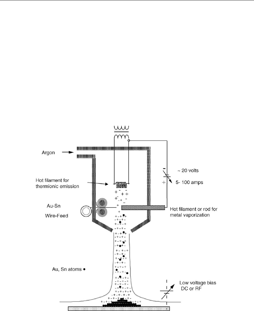
Shown in Figure 18.6, this is the mainstay used at JPC for commercial production of solder
coatings [6, 11]; AuSn can serve as an example. A fine wire of AuSn alloy is fed continuously
Figure 18.6: This deposition source combines the main features of the hot filament wirefeed and
the e-jet plasma JVD sources. High argon ion density permits substrate cleaning, as well as ion
bombardment of the growing film at low energy and high current.
